EP1858066A2 - Halbleiterbauelemente - Google Patents
Halbleiterbauelemente Download PDFInfo
- Publication number
- EP1858066A2 EP1858066A2 EP07010043A EP07010043A EP1858066A2 EP 1858066 A2 EP1858066 A2 EP 1858066A2 EP 07010043 A EP07010043 A EP 07010043A EP 07010043 A EP07010043 A EP 07010043A EP 1858066 A2 EP1858066 A2 EP 1858066A2
- Authority
- EP
- European Patent Office
- Prior art keywords
- semiconductor
- substrate
- semiconductor device
- electrodes
- doping
- Prior art date
- Legal status (The legal status is an assumption and is not a legal conclusion. Google has not performed a legal analysis and makes no representation as to the accuracy of the status listed.)
- Withdrawn
Links
Images





Classifications
-
- H—ELECTRICITY
- H10—SEMICONDUCTOR DEVICES; ELECTRIC SOLID-STATE DEVICES NOT OTHERWISE PROVIDED FOR
- H10D—INORGANIC ELECTRIC SEMICONDUCTOR DEVICES
- H10D64/00—Electrodes of devices having potential barriers
- H10D64/60—Electrodes characterised by their materials
- H10D64/64—Electrodes comprising a Schottky barrier to a semiconductor
- H10D64/647—Schottky drain or source electrodes for IGFETs
-
- H—ELECTRICITY
- H10—SEMICONDUCTOR DEVICES; ELECTRIC SOLID-STATE DEVICES NOT OTHERWISE PROVIDED FOR
- H10D—INORGANIC ELECTRIC SEMICONDUCTOR DEVICES
- H10D30/00—Field-effect transistors [FET]
- H10D30/01—Manufacture or treatment
- H10D30/021—Manufacture or treatment of FETs having insulated gates [IGFET]
- H10D30/027—Manufacture or treatment of FETs having insulated gates [IGFET] of lateral single-gate IGFETs
- H10D30/0277—Manufacture or treatment of FETs having insulated gates [IGFET] of lateral single-gate IGFETs forming conductor-insulator-semiconductor or Schottky barrier source or drain regions
Definitions
- the present invention relates to semiconductor devices comprising metal-semiconductor compound/semiconductor junction regions, e.g. metal-silicide/semiconductor or metal-germanide/semiconductor junction regions.
- the invention is related to semiconductor devices, such as e.g. field effect transistors, comprising at least one rectifying or Schottky barrier contact used as first and/or second electrodes, e.g. as source/drain electrodes.
- Highly doped semiconductor regions also known as source/drain regions, are used to obtain a low ohmic contact towards the interconnect levels and towards the channel and to create a junction between such highly doped regions and the channel for blocking carrier transport when the transistor is in the off-state.
- these semiconductor regions tend to be replaced by metallic regions, formed by metallic electrodes. These metallic electrodes directly contact the semiconductor channel thereby forming a metallic-semiconductor junction which is known as a rectifying contact or Schottky barrier junction.
- Metallic regions offer advantages such a good contact with the interconnect level, low series resistance towards the channel and a low capacitance towards the bulk, because of their shallow and well-defined geometry. For reasons of reduced process complexity these metallic regions are often formed by silicidation of the semiconductor regions at the location of the source and/or drain region.
- US patent US 6,495,882 discloses a MOSFET device wherein Schottky barrier contacts are utilized as source and/or drain contacts to eliminate the requirement for halo/pocket implants and shallow source/drain extensions for control of short channel effects.
- the thus obtained metallic-semiconductor junction is characterized by a potential barrier, the height of which depends on the properties of the metallic material and of the semiconductor material constituting the junction. If this barrier height is high, i.e. higher than 300 meV, not only will the transistor have a low on-current, being limited by the tunneling of carriers through this high potential barrier, but also they will have a poor sub-threshold behavior.
- the Schottky barrier height should be less than 200 meV for p-type Schottky barrier field effect transistor (SBFET) and less than 150 meV for n-type SBFET.
- SBFET p-type Schottky barrier field effect transistor
- Platinum silicide and Ytterbium silicide are reported to provide the lowest Schottky barrier height of about 250 meV for respectively p-type SBFET and n-type SBFET.
- the semiconductor devices according to embodiments of the invention show good short channel behaviour and good performance.
- the method according to embodiments of the invention leads to good semiconductor devices, such as Field-effect transistors (SBFETs), with limited process complexity.
- semiconductor devices such as Field-effect transistors (SBFETs)
- the method according to embodiments of the invention leads to a device with high on-current by lowering a potential barrier height of a rectifying contact formed by a metal-semiconductor compound/metal interface, e.g. a silicide/semiconductor or germanide/semiconductor interface, between a first and/or second electrode and a semiconductor region of the device, also referred to as Schottky barrier height.
- a metal-semiconductor compound/metal interface e.g. a silicide/semiconductor or germanide/semiconductor interface
- the present invention provides a semiconductor device having first and second electrodes formed in a semiconductor substrate having a doping level, the first and second electrodes being separated from each other by a semiconductor region, and a third electrode for controlling conductivity of the semiconductor region, at least one of the first and second electrodes forming a rectifying contact with the semiconductor region, also called a Schottky contact or a Schottky-like contact, the rectifying contact having a potential barrier, wherein the semiconductor region is uniformly doped at least in a horizontal direction between the first and the second electrode, but preferably also in a vertical direction i.e. in a direction perpendicular to the third electrode, so as to have a doping level higher than the doping level of the semiconductor substrate and so as to, in operation, induce an image-force mechanism for lowering the potential barrier of the at least one rectifying contact.
- direction perpendicular to the third electrode is meant in a direction substantially perpendicular to the plane of the substrate.
- An advantage of the semiconductor device according to embodiments of the invention is that its shows good short channel behaviour, good performance and high on-current.
- the semiconductor device may be a Schottky barrier field-effect transistor (SBFET) comprising a gate electrode isolated from a semiconductor channel by a gate dielectric, source and drain electrodes being aligned to the gate electrode and located at opposite sides of the semiconductor channel. At least one of the source/drain electrodes forms a Schottky contact or Schottky-like contact or rectifying contact with the semiconductor channel.
- the semiconductor channel is substantially uniformly doped along its length and at least along the depth of the at least one Schottky contact or Schottky-like contact or rectifying contact.
- the doping level in the semiconductor channel is selected such that, in operation, the potential barrier, also referred to as Schottky barrier, of the at least one Schottky contact or Schottky-like contact or rectifying contact is substantially reduced by an induced image-force mechanism.
- the potential barrier also referred to as Schottky barrier
- the doping level of the semiconductor region may be between 1e16 cm -3 and 1 e18 cm -3 . If the uniform channel doping concentration is too low, i.e. substantially below 1e16 cm -3 , no substantial image force effect will occur. If the uniform channel doping concentration is too high, i.e. substantially above 1e18 cm -3 , the effect of mobility degradation and even short-circuiting of the channel with the source/drain regions at higher channel doping levels will be dominant.
- the semiconductor region may have a length and the rectifying contact may have a depth into the semiconductor substrate and the semiconductor region may be uniformly doped along its length and at least along the depth of the rectifying contact.
- At least one of the first or second electrode may comprise a metal-semiconductor compound.
- At least one of the first or second electrode, optionally both the first and the second electrode, may comprise a silicide.
- At least one of the first or second electrode, optionally both the first and the second electrode, may comprise a germanide.
- the semiconductor device may be a p-type semiconductor device.
- at least one of the first and second electrodes may comprise platinum silicide.
- the semiconductor region may be uniformly doped with one or more dopant elements selected from group V elements.
- the semiconductor device may be an n-type semiconductor device.
- at least one of the first and second electrodes may comprise Ytterbium silicide.
- the semiconductor region may be uniformly doped with one or more dopant elements selected from group III elements.
- the semiconductor substrate may be a silicon substrate.
- a method for manufacturing a semiconductor device comprises:
- direction perpendicular to the third electrode is meant in a direction substantially perpendicular to the plane of the substrate.
- An advantage of the method according to embodiments of the invention is that it has limited complexity and it leads to a semiconductor device showing good short channel behaviour, good performance and high on-current.
- the method of modulating, in particular reducing, the height of the potential barrier of the at least one rectifying contact by means of an image-force lowering effect can be easily implemented in state-of-the-art semiconductor manufacturing processes as it relies on conventional CMOS process techniques such as ion implantation to adjust the concentration of dopant elements of the semiconductor region, e.g. channel, to an appropriate level, which is substantially uniform over the channel both in lateral and in vertical direction.
- CMOS process techniques such as ion implantation to adjust the concentration of dopant elements of the semiconductor region, e.g. channel, to an appropriate level, which is substantially uniform over the channel both in lateral and in vertical direction.
- the method may be a method for manufacturing a Schottky barrier field-effect transistor (SBFET).
- the method may comprise providing a semiconductor substrate, forming a doped region in the semiconductor substrate, forming a gate electrode on the doped region, forming two electrodes in the semiconductor substrate aligned to and located at opposite sides of the doped region, at least one of the electrodes forming a Schottky contact or Schottky-like contact or rectifying contact with the doped region, the doped region being substantially uniformly doped in-between the two electrodes and at least along the depth of the at least one Schottky contact or Schottky-like contact or rectifying contact.
- the doping level is selected such that, in operation, the potential barrier of the at least one Schottky contact or Schottky-like contact or rectifying contact is reduced by an image-force mechanism.
- uniformly doping the semiconductor region may be performed up to a concentration of between 1 e16 cm -3 and 1 e18 cm -3 . If the uniform channel doping concentration is too low, i.e. below 1e16 cm -3 , no substantial image force effect will occur. If the uniform channel doping concentration is too high, i.e. above 1e18 cm -3 , the effect of mobility degradation and even short- circuiting of the channel with the source/drain regions at higher channel doping levels will be dominant.
- Uniformly doping the semiconductor region may be performed by implanting dopant elements.
- Embodiments of the present invention provide a semiconductor device having first and second electrodes formed in a semiconductor substrate having a doping level, the first and second electrodes being separated from each other by a semiconductor region, and a third electrode for controlling conductivity of the semiconductor region, at least one of the first and second electrodes forming a rectifying contact with the semiconductor region, the rectifying contact having a potential barrier, wherein the semiconductor region is uniformly doped at least in a horizontal direction between the first and the second electrode, but preferably also in a vertical direction i.e. in a direction perpendicular to the third electrode, to have a doping level higher than the doping level of the semiconductor substrate and so as to, in operation, induce an image-force mechanism for lowering the at least one Schottky contact.
- direction perpendicular to the third electrode is meant in a direction substantially perpendicular to the plane of the substrate.
- An advantage of the semiconductor device according to embodiments of the invention is that it shows good short channel behaviour, good performance and high on-current.
- the semiconductor device may be a p-type or an n-type device.
- the semiconductor device being a p-type Schottky barrier field effect transistor (SBFET) having source and drain electrodes with a channel in between, and a gate electrode.
- SBFET Schottky barrier field effect transistor
- the invention is not limited thereto.
- a person skilled in the art will realize that the teaching of embodiments of the invention is also applicable to n- type Schottky barrier field effect transistors as well.
- MOSFET metal oxide semiconductor field effect transistor
- a third electrode e.g. a control electrode such as a gate electrode
- at least one of these two electrodes e.g. first and second main electrode such as source and drain electrodes, forms a Schottky contact, a Schottky-like contact or rectifying contact, also referred to as Schottky barrier, with the semiconductor region, e.g. channel.
- Examples may include, but are not limited to, CMOS, BICMOS, Bipolar and SiGe BICMOS. Examples of such transistors may, for example, be enhancement type FET, depletion type FET, junction FET (JFET), ....
- doping of this semiconductor region is performed and is selected to lower the Schottky barrier height of this Schottky-like contact by inducing an image-force mechanism (see further).
- At least one of the source and drain electrodes may be formed of a metal-semiconductor compound such as a silicide or a germanide.
- a metal-semiconductor compound such as a silicide or a germanide.
- SBFET p-type Schottky barrier field effect transistor
- PtSi platinum silicide
- Yb, Er, Pd can also be used to form the source/drain regions.
- the choice of the metal-semiconductor-forming metals, e.g. silicide-forming material, will depend on the type of semiconductor device, e.g. transistor, to be formed (n-type or p-type) and on the Schottky barrier height to be obtained.
- the present invention also applies to semiconductor devices comprising source and drain electrodes of which at least one is formed of a different metal-semiconductor compound, such as for example a germanide or a germanosilicide.
- n-type or p-type dopants depending on the kind and type of semiconductor device to be formed, can be used such as, for example, In, B or As.
- Embodiments of the present invention will further be described by means of a silicon substrate.
- various semiconductor substrates are available to which the teaching of the invention can be applied such as, for example, germanium (Ge) substrates, silicon-on-insulator (SOI) substrates, germanium-on-insulator (GOI) substrates, substrates with a channel region comprising silicon and/or germanium, substrates with strained channels.
- Fig. 1 shows a schematic lateral cross-section of a Schottky barrier field effect transistor (SBFET) 1 according to an embodiment of the present invention.
- the SBFET 1 comprises a conductive control electrode, e.g. gate electrode 3, electrically separated from a semiconductor substrate 2 by a control electrode dielectric, e.g. gate dielectric 4.
- first and second main electrodes e.g. source/drain electrodes 6 are present. At least one of the source/drain electrodes 6 forms a Schottky contact or rectifying contact to a semiconductor channel 5 which is located in the substrate 2 and in-between both source/drain regions 6.
- the at least one Schottky contact may also be referred to as source/drain junction or as metal-semiconductor compound/ semiconductor junction, in particular for the example given a metal-silicide/semiconductor junction.
- Schottky contact Schottky barrier, Schottky-like contact, Schottky diode, rectifying contact, source/drain junction, metal-semiconductor compound/semiconductor junction or metal-silicide/semiconductor junction, the same thing is meant, i.e. for the example discussed the metal or metal-silicide/semiconductor interface formed between the source/drain regions 6 and the channel 5.
- a rectifying contact is the metal-semiconductor contact which displays asymmetric current-voltage characteristics, i.e. it allows high current to flow across under a forward bias condition and it blocks current off under a reverse bias condition. This behaviour is controlled by bias voltage dependent changes of the potential barrier height in the contact region.
- sidewall spacers 13 may be present lying against the stack formed by the gate electrode 3 and the gate dielectric 4.
- Fig. 2 schematically shows a flow chart of a fabrication process of a SBFET 1 according to a preferred embodiment of the present invention. This figure illustrates relevant process steps for a possible manufacturing sequence.
- Fig. 3 to 5 illustrate cross-sections of the SBFET 1 according to subsequent steps in the manufacturing process according to this preferred embodiment. It is to be understood that the illustrated manufacturing method is only an example and is not intended to limit the invention. For example, the method may comprise another sequence of process steps or may comprise more or less process steps. Furthermore, the method may also use other materials or processes.
- the method according to embodiments of the invention may be used for manufacturing SBFETs in sub 32 nm CMOS technology, for example in sub 22 nm CMOS technology, i.e. technology where minimal length of devices is about 32 nm respectively 22 nm.
- an n-type (100) silicon substrate 2 is provided (step 10 in Fig. 2), preferably with a resistivity in the range of between 2.5 and 8.5 ⁇ .cm.
- the substrate may be undoped, or may have a doping level of 5e15 cm -3 in case of bulk substrates or 1e15 cm -3 in case of SOI substrates.
- Isolation regions 7 are formed in the substrate 2 to provide a pattern of active regions 8 wherein the SBFETs 1 are to be formed (see Fig. 3; see step 20 in Fig. 2).
- the isolation regions 7 isolate neighbouring SBFETs 1 on the substrate 2.
- the method will be described by means of only one SBFET 1.
- the isolation regions 7 may be formed by shallow trench isolation (STI).
- STI isolation regions 7 may be formed by initially creating a shallow trench in the silicon substrate 2, e.g. by a conventional photolithographic and anisotropic dry etch process such as a reactive ion etching (RIE) procedure, using e.g. CI 2 as an etchant.
- RIE reactive ion etching
- the shallow trench is created to a depth of for example between about 200 to 600 nm in the silicon substrate 2.
- a silicon oxide layer is deposited, for example by a low pressure chemical vapour deposition (LPCVD) procedure or by a plasma enhanced chemical vapour deposition (PECVD) procedure, to a thickness between about 300 to 1500 nm.
- LPCVD low pressure chemical vapour deposition
- PECVD plasma enhanced chemical vapour deposition
- the shallow trenches are thus completely filled.
- Removal of the silicon oxide from regions other than inside the shallow trenches is accomplished using either a chemical mechanical polishing (CMP) procedure, or via a RIE procedure using a suitable etchant, resulting in insulator filled STI regions 7.
- CMP chemical mechanical polishing
- the isolation regions 7 may also comprise LOCOS (local oxidation of silicon) regions. These LOCOS regions 7 may be formed via initially forming an oxidation resistant mask, such as silicon nitride, then exposing regions of the semiconductor substrate not protected by the silicon nitride masking pattern, to a thermal oxidation procedure. LOCOS regions 7 are thus created at a thickness equal to the depth of STI regions 7. After formation of the LOCOS regions 7, the oxidation resistant mask is removed.
- LOCOS local oxidation of silicon
- the active regions 8 of the substrate 2 are doped, e.g. implanted with dopant elements (indicated with arrows 9 in Fig. 3) to form a well region 11 in the substrate 2 (step 30 in Fig. 2; Fig. 3).
- dopant elements e.g. implanted with dopant elements (indicated with arrows 9 in Fig. 3) to form a well region 11 in the substrate 2 (step 30 in Fig. 2; Fig. 3).
- the kind of dopant elements used depends on the type of semiconductor device 1, in the example given SBFET 1, to be formed.
- dopant elements selected from group V elements may be used, such as e.g. P and/or As.
- n-type devices 1 preferably one or more dopant elements selected from group III elements may be used, such as e.g. In and/or B.
- Doping may be performed by any suitable technique known by a person skilled in the art, such as, for example, by ion implantation or by plasma doping. According to the present invention, doping of the channel 5 is performed such that an image-force mechanism is induced (see further) which lowers the potential barrier of the Schottky contact between at least one of the source/drain electrodes 6 and the channel 5, also referred to as Schottky barrier.
- a dielectric layer which will later on serve as gate dielectric 4, may be deposited onto the substrate 2 followed by deposition of a conductive layer, e.g. boron-doped polycrystalline silicon layer, which will be used to form gate electrode 3.
- the dielectric layer may comprise a single dielectric layer, such as a semiconductor oxide or oxynitride, e.g. SiO 2 , SiON, a high-k dielectric such a hafnium silicate or hafnium oxide, or a stack of dielectric layers, such as a high-k dielectric and a semiconductor oxide, e.g.
- the conductive layer may, for example, comprise a metal such as TiN or TaN or may comprise any other suitable conductive material.
- the dielectric layer and the conductive layer form a stack.
- the stack of the dielectric layer and the conductive layer may then be patterned, e.g. lithographically patterned, to form a gate stack 3, 4 of the SBFET 1 (step 40 in Fig. 2; see Fig. 4).
- the dielectric layer and the conductive layer are patterned in one step to form a gate stack 3, 4 comprising a gate dielectric 4 and gate electrode 3 having a same width.
- the dielectric layer and the conductive layer may be separately patterned so as to form a gate dielectric 4 and a gate electrode 3 having a different width, as can be seen in Fig. 1.
- source/drain regions 6 of the SBFET 1 are formed by doping, e.g. by implanting dopant elements as indicated by arrows 12 in Fig. 4.
- sidewall spacers 13 may be formed against the gate stack 3, 4 by, for example, anisotropically etching back a thin dielectric layer, e.g. silicon nitride layer, which is uniformly deposited over the substrate 2 (step 50 in Fig. 2).
- a metal layer e.g. a platinum layer, is deposited over the substrate 2, followed by a silicidation step to silicidise the source/drain regions 6 so as to form source/drain electrodes 6.
- silicidation of the source/drain regions 6 is performed by performing a rapid thermal anneal step (RTP) at about 550°C.
- RTP rapid thermal anneal step
- unreacted metal e.g. platinum
- the gate electrode 3 may be silicided.
- the source/drain regions 6 may be silicided to form source/drain electrodes 6, while the gate electrode 3 is not silicided. Therefore, in this case, before deposition of the metal layer, e.g. platinum layer, a mask may be provided onto the gate electrode 3 (not illustrated).
- the source/drain regions 6 and the gate electrode 3 may be silicided in different steps and with different silicide-forming metals.
- a mask may be provided onto the gate electrode 3 before depositing the first silicide-forming metal layer, e.g. platinum layer.
- the first silicide-forming metal layer e.g. platinum layer.
- a mask may be provided on these regions 6 before a layer of a second silicide-forming metal is provided for silicidation of the gate electrode 3. Due to lateral diffusion of the formed silicide, e.g. PtSi, under the spacers 11 during the silicidation step, the source/drain electrodes 6 formed are substantially aligned to the gate stack 3, 4.
- the resulting SBFET 1, formed using the method according to the present embodiment, may comprise source/drain electrodes 6 with a thickness t of, for e.g. sub 32 nm or sub 22 nm CMOS technology, less than 200 nm, preferably less than 150 nm (see Fig. 5).
- the method according to embodiments of the invention leads to a SBFET 1 with source/drain electrodes 6, in the example given, PtSi/n-Si junctions which behave as Schottky barriers or, in other words, form Schottky diodes.
- source/drain electrodes 6 in the example given, PtSi/n-Si junctions which behave as Schottky barriers or, in other words, form Schottky diodes.
- electrons coming from a source/drain electrode 6 and going to the channel 5 experience a potential barrier which they have to overcome before they can flow to the channel 5.
- the Schottky barrier may be lower than when no additional doping is performed. This will further be described and illustrated hereinafter.
- the doping level of the channel 5 is increased although it would be expected that the mobility of charge carriers will hereby be degraded.
- this mobility degradation is compensated for more than expected by the decrease in barrier height such that the drive current remains high and is thus not substantially influenced by increasing the doping level.
- the shift in threshold voltage V t due to the increased channel doping can be controlled by an appropriate choice of material for forming the gate electrode, in particular the choice of workfunction of that material.
- the contribution of the increased channel doping to the threshold voltage V t may then be compensated for by a decreased workfunction of the gate electrode.
- a doping step is performed for intentionally doping or controlling dopant concentration in the channel 5 of the SBFET 1.
- both hole barrier heights and electron barrier heights will be discussed. Both these barriers are relevant in both p-type and n-type devices.
- the barrier related to minority carriers of a channel 5 controls the drive current, also referred to as on-current, while the barrier related to majority carriers of a channel 5 controls the leakage current, also referred to as off-current.
- the drive current also referred to as on-current
- the barrier related to majority carriers of a channel 5 controls the leakage current, also referred to as off-current.
- electrons create leakage current in the channel 5
- holes create drive current in the channel 5.
- a silicon substrate 2 was divided into two parts, a first part and a second part, also respectively referred to as south well and north well. Dividing the substrate 2 into two parts is only for the ease of comparison.
- the first part or south well of the substrate 2 is then additionally doped with dopant elements to form a well region 11 in the substrate 2, part of which will later form the channel 5 of the SBFET 1.
- P 3e12 cm -2 , I20 KeV
- a combination of P (3e12 cm -2 , 120 KeV) and As (1e12 cm -2 , 90 keV) was used (see further) to dope the active regions 8.
- the second part or north well of the substrate 2 was not doped before the SBFET 1 was formed on it.
- SBFETs 1 were then formed on both the first and second part of the substrate 1 as described above.
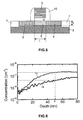
- Fig. 6 shows a simulated dopant element profile of the channel 5 of the SBFET 1 formed on the first part of the substrate 2 for the two different doping conditions, i.e. for P (curve 13) and for P/As (curve 14).
- concentration of the dopant elements defined by the number of dopant elements per cm 3 , is given as a function of the depth into the substrate 2. This depth is measured from the surface of the substrate 2 on which the SBFET 1 is formed, or in other words from which the substrate 2 is doped (0 nm) towards the bulk of the substrate 2.
- the vertical location i.e.
- the depth d in the substrate 2, of the metal-semiconductor compound/semiconductor interface, in the example given the PtSi/n-Si interface, is indicated (vertical dashed line in Fig. 6). It can be seen that, according to the present example, the PtSi/n-Si interface is located at a depth d of about 50 nm from the gate dielectric 4 or substrate surface. At this depth d the concentration is about 2e17 cm -3 for the P/As doped substrates 2 and about 5e16 cm -3 for the P doped substrates 2.
- Capacitance-voltage measurements on the SBFET devices 1 formed indicate a doping level of 1e16 cm -3 in the second part or north well (which was not additionally doped before formation of the SBFET 1) and of 8e16 cm -3 or 2e17 cm -3 in the first part or south well (which was doped respectively with P or with P/AS before formation of the SBFET).
- the electrical equivalent oxide thickness (EOT) of the SiON gate dielectric 4 extracted from these capacitance voltage curves is determined at about 2 nm.
- the lateral width of the SiN spacers 5 is about 11 nm. This may, for example, be determined by Scanning Electron Microscopy (SEM).
- the height of the potential barrier formed also referred to as Schottky barrier height can be determined from the current flowing through the junction during biasing.
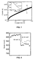
- Fig. 7 shows typical current voltage curves measured on two PtSi/n-Si diodes of 100 ⁇ m x 100 ⁇ m in substrates 1 with different dopant concentration, i.e.
- a Schottky contact is formed on a first main surface.
- a metal contact is formed on a second main surface opposite to the first main surface. This metal contact serves as a contact location for a probe for measuring the Schottky barrier. Hence, the Schottky barrier is measured through the substrate and thus there is a long current path, which may lead to high parasitic series resistance.
- the Norde function F(V) is plotted for the second part or north well (not additionally doped, curve 17) in the inset of Fig. 7. This plot is then used to determine the Schottky barrier height for the PtSi/n-Si interface.
- a set of electron Schottky barrier heights of PtSi/n-Si source/drain junctions determined as described above is plotted in Fig. 8.
- Schottky barrier junctions were measured in a statistical manner, i.e. measurements were performed along a straight line on the substrate 2, for both the first and second part of the substrate 2. From the left part of Fig. 8 it can be seen that the electron barrier height or Schottky barrier height (SBH) of the north well diodes (second part of the substrate 2, not additionally doped) is almost constant along the line of measurement and has an average value close to 870 meV. In the south well (first part of the substrate 2, additionally doped), the values of the SBH are a function of the dopant concentration.
- the average value of the SBH is around 840 meV for the 8e16 cm -3 doped substrate (only P-doped) and 820 meV when the doping concentration is 2e17 cm -3 (P/As doped) (see right part of Fig. 8).
- the fluctuation on the Schottky barrier height determined for the south well junctions (first part of the substrate 2, additionally doped) can be due to variations of the thickness t of PtSi (see Fig. 5) in the non-doped substrate.
- barrier fluctuations can be reduced or minimized by improving the uniformity of the substrate doping, for example by increasing the doping level or by using plasma doping instead of ion implantation, at least in the channel region close to the silicide-semiconductor junction, and/or by reducing the variation of thickness t of the silicide regions 6.
- the latter is related to control of process technology and may be performed by e.g. control of the thickness of the layer of metal-semiconductor compound forming metal, e.g. silicide forming metal, during deposition (e.g. by plasma vapour deposition (PVD)), treatment of surface (cleaning, pre-amorphization), thermal budget controlling diffusion of silicide-forming species, ....
- the difference in barrier height between PtSi/n-Si junctions formed in the first part of the substrate 2 (additionally doped) and junctions formed in the second part of the substrate 2 (not additionally doped) increases when the dopant concentration is increased.
- the Schottky barrier height is reduced by about 30 meV when the dopant level is 8e16 cm -3 in the first part and 1e16 cm -3 in the second part of the substrate 2 (open circles in Fig. 8) while the Schottky barrier height is reduced by about 50 meV when the dopant level is 2e17 cm -3 in the first part and 1e16 cm -3 in the second part of the substrate 2 (filled squares in Fig. 8).
- E max q ⁇ N D ⁇ 2 ⁇ ⁇ i - V a ⁇ s
- ND the dopant concentration
- ⁇ i the built-in potential
- V a the applied voltage
- ⁇ s the permittivity of the semiconductor.
- the potential energy band diagram of the source/drain electrode 6, i.e. PtSi, is given, while on the right the potential energy band diagram of the doped n-type semiconductor channel 5, in the example given n-Si channel 5, is given for the situation of thermal equilibrium.
- PtSi the potential energy band diagram of the source/drain electrode 6, i.e. PtSi
- the potential energy band diagram of the doped n-type semiconductor channel 5, in the example given n-Si channel 5 is given for the situation of thermal equilibrium.
- an electron from the n-Si channel 5 approaches the PtSi/n-Si interface, it will exert an electrostatic force on the charges (free electrons) in the PtSi. In that way, a 'hole', or more correctly a locally decreased electron concentration, may be induced by the repulsing force of the electron from the n-Si channel 5.
- This 'hole' forms the mirror image of the electron in the n-Si channel 5 and will exert a force. By this force, the electron will have a negative potential energy with respect to an electron at infinite distance. This potential energy caused by the mirror image must be added to the potential energy of the Schottky barrier. The result of this phenomenon is a lowering of the potential barrier height.
- the barrier height itself that is being reduced, while the band bending in the semiconductor region 5 remains substantially unaffected.
- the barrier height itself is reduced thermo-ionic emission of carriers from the metal-semiconductor compound region, e.g; silicide region 6, to the channel 5 over the barrier is more likely to occur at a given temperature.
- this barrier height reduction is small compared to the barrier height itself, this reduction is of interest as it depends on the voltage applied over the silicide-semiconductor interface resulting in a voltage dependent reverse bias current.
- the absolute value of the barrier may be below 200 meV. In other words, the drive current of the field effect transistor in the on-state will progressively increase with increasing drain-to-channel voltage.
- MEDIC1 TCAD software from Synopsys
- the electric field E increases with the forward bias voltage applied over the Schottky barrier junction and thus the effective Schottky barrier lowering, which is calculated for a relatively low voltage of 50 mV in Table 1, will be even more enhanced when the device is in the on-state.
- the Schottky barrier height will even further decrease resulting in a further improvement of the transistor current when the transistor is in the on-state.
- the source current I s versus gate voltage V g curve and the drain current I d versus gate voltage V g curve of p-type SBFETs 1 formed in the second part of the substrate 2 or north well (1e16 cm -3 , open squares, not additionally doped) and the first part of the substrate 2 or south well (additionally doped, 2e17 cm -3 , filled circles) are represented in Fig. 10(a) and 10(b) respectively. These curves are measured on 1 ⁇ m channel length SBFETs 1 at a drain voltage V d of -0.05 V (lower curves) or -1 V (upper curves).
- the sub-threshold slope S of the I s -V g transfer characteristic of the SBFETs 1 in the first part of the substrate 2 or south well is about 70 mV/dec, with a ratio I on /I off between the transistor current in the on-state I on and the transistor current in the off sate I off of about 10 7 .
- the increased channel doping not only provides a lower Schottky barrier height and a steep single sub-threshold slope, but also a substantial reduction of the drain-induced-barrier-lowering effect (DIBL) which in its turn reduces the leakage current of the transistor.
- DIBL drain-induced-barrier-lowering effect
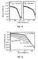
- Fig. 11 (a) and 11 (b) show simulated (solid line) and measured (open circles) I s -V g transfer characteristics of the SBFETs 1 for a substrate doping N D of 2e7 cm -3 (Fig. 11 (a)) and of 1e16 cm -3 (Fig. 11(b))).
- the I s -V g transfer characteristics are measured with a drain voltage of -1.1 V.
- Curves simulated with MEDIC1 simulation software of SYNOPSIS and measured transfer curves are, as shown in Fig. 11 (a) and 11 (b), in good agreement.
- a single sub-threshold slope SS of 66 mV/dec is present in the curve for obtaining a drive current of about 1e-5 A/ ⁇ m.
- the transfer curve I s -V g is characterised by a single sub-threshold slope S due to sub-threshold thermo-ionic emission.
- Fig. 12 shows a simulated transfer characteristic for a 1 ⁇ m channel length SBFET 1 with a channel doping of 1e16 cm -3 and a drain voltage of -1.1 V while the source is biased to 0 V.
- the hole barrier height which determines the drive current, also referred to as on-current, of the p-type SBFET 1 is used as a parameter to simulate the drive current vs gate voltage. Therefore, the effective hole Schottky barrier height is varied from 260 meV to 210 meV.).
- the drive current is increased thanks to the Schottky barrier lowering effect.
- the overall effect of increased substrate doping N D is observed to be an increased drive current through image-force barrier lowering effect.
- Fig. 14 shows a measured transfer curve, i.e. source current I s versus gate voltage V g , for SBFETs 1 with a channel length of 1 ⁇ m with a drain voltage of -1.1 V for three different substrate doping levels, i.e. 1e16 cm -3 (curve 19), 1e18 cm -3 (curve 21) and 1e19 cm -3 (curve 22).
- the Schottky barrier height is simulated to be the same for the three doping levels. If the uniform channel doping concentration is too low, i.e. below 1e16 cm -3 , no substantial image force effect will occur. If the uniform channel doping concentration is too high, i.e. above 1e18 cm -3 , the effect of mobility degradation and even short-circuiting of the channel 5 with the source/drain regions 6 at higher channel doping levels will be dominant.
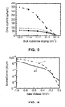
- Fig. 15 shows a simulated drive current I s as a function of the substantial uniform channel doping for a field effect transistor with conventional doped source/drain regions 6 (filled squares) and with Schottky barrier source/drain regions 6 for a barrier height of 190 meV (filled triangles) or 250 meV (filled circles).
- Schottky barrier lowering effect according to the present invention was hereby taken into account.
- the substrate or channel doping concentrations also influence the performance of short channel SBFET 1.
- the simulated transfer characteristic I s -V g of two bulk SBFETs having a gate length L of 100 nm and a substrate doping N D of respectively 1e16 cm -3 (solid line, curve 23) and 1e18 cm -3 (dashed line, curve 24) is shown in Fig. 16. Taking into account the Schottky barrier lowering effect and the difference in threshold voltage due to the different channel doping, a higher drive current is obtained for the higher-doped SBFET 1.
- Fig. 17 shows a simulated transfer characteristic I s -V g for p-type (Fig. 17(a)) and for n-type (Fig. 17(b)) SBFETs 1 manufactured on an SOI substrate 2 with a silicon body thickness of I0 nm and a silicide thickness of about 4 nm.
- PtSi was used to form the metallic source/drain regions 6 for the p-type SBFET 1
- YbSi may be used to form source/drain regions 6 for an n-type SBFET 1.
- the SBFETs 1 have a gate length L of 100 nm and a substrate doping N D of respectively 1e16 cm -3 (solid line, curve 25) and 1e18 cm -3 (dashed line, curve 26). Taking into account the Schottky barrier lowering effect and the difference in threshold voltage due to the different channel doping, again a higher drive current is obtained for the higher-doped SBFET 1.
- the present application thus demonstrates, in one of its embodiments, that the Schottky barrier height for holes in PtSi/n-Si junctions can be lowered by increasing the n-Si channel doping to an appropriate dopant level resulting in an image-force mechanism. Because of the lowering of the Schottky barrier height a substantial gain of the drive current in long-channel bulk p-type SBFETs may be obtained.
- a channel dopant concentration of 2e17 cm -3 obtained by the combined ion implantation of P (3e12 cm -2 , I20 KeV) and As (1e12 cm -2 , 90KeV) can be used to lower the hole Schottky barrier height by more than 50 meV, while the drive current of the corresponding 1 ⁇ m channel length SBFET 1 is increased by a factor of 2.
- the method according to embodiments of the invention may be used to lower the electron Schottky barrier height for n-type semiconductor devices 1.
- the disclosed method of modulating the Schottky barrier height by means of an image force lowering effect can be easily implemented in state-of-the-art semiconductor manufacturing processes as it relies on the conventional CMOS process techniques such as ion implantation to adjust the dopant of the substrate to an appropriate level, which is substantially uniform over the channel both in lateral and in vertical direction.
Landscapes
- Electrodes Of Semiconductors (AREA)
- Thin Film Transistor (AREA)
- Insulated Gate Type Field-Effect Transistor (AREA)
Applications Claiming Priority (1)
| Application Number | Priority Date | Filing Date | Title |
|---|---|---|---|
| US80195606P | 2006-05-19 | 2006-05-19 |
Publications (2)
| Publication Number | Publication Date |
|---|---|
| EP1858066A2 true EP1858066A2 (de) | 2007-11-21 |
| EP1858066A3 EP1858066A3 (de) | 2009-07-01 |
Family
ID=38291219
Family Applications (1)
| Application Number | Title | Priority Date | Filing Date |
|---|---|---|---|
| EP07010043A Withdrawn EP1858066A3 (de) | 2006-05-19 | 2007-05-21 | Halbleiterbauelemente |
Country Status (3)
| Country | Link |
|---|---|
| US (1) | US20070267762A1 (de) |
| EP (1) | EP1858066A3 (de) |
| JP (1) | JP2007329472A (de) |
Families Citing this family (10)
| Publication number | Priority date | Publication date | Assignee | Title |
|---|---|---|---|---|
| CN101621030B (zh) * | 2008-07-02 | 2011-01-12 | 中芯国际集成电路制造(上海)有限公司 | 具有多晶硅接触的自对准mos结构 |
| JP2010161259A (ja) * | 2009-01-09 | 2010-07-22 | Toshiba Corp | プロセスシミュレーションプログラム、プロセスシミュレーション方法、プロセスシミュレータ |
| WO2011068016A1 (en) * | 2009-12-04 | 2011-06-09 | Semiconductor Energy Laboratory Co., Ltd. | Semiconductor device |
| US8415748B2 (en) * | 2010-04-23 | 2013-04-09 | International Business Machines Corporation | Use of epitaxial Ni silicide |
| US8513765B2 (en) * | 2010-07-19 | 2013-08-20 | International Business Machines Corporation | Formation method and structure for a well-controlled metallic source/drain semiconductor device |
| GB201202128D0 (en) * | 2012-02-08 | 2012-03-21 | Univ Leeds | Novel material |
| US20130241007A1 (en) * | 2012-03-15 | 2013-09-19 | International Business Machines Corporation | Use of band edge gate metals as source drain contacts |
| US9590611B2 (en) * | 2014-04-10 | 2017-03-07 | The United States Of America As Represented By The Secretary Of The Navy | Radiation-hardened dual gate semiconductor transistor devices containing various improved structures including MOSFET gate and JFET gate structures and related methods |
| DE102015102055A1 (de) * | 2015-01-16 | 2016-07-21 | Infineon Technologies Ag | Verfahren zum Bearbeiten einer Halbleiteroberfläche |
| CN112234102B (zh) * | 2020-10-26 | 2025-05-30 | 长沙理工大学 | 一种SiC基纳米尺度肖特基势垒场效应晶体管 |
Family Cites Families (3)
| Publication number | Priority date | Publication date | Assignee | Title |
|---|---|---|---|---|
| US6974737B2 (en) * | 2002-05-16 | 2005-12-13 | Spinnaker Semiconductor, Inc. | Schottky barrier CMOS fabrication method |
| US6744111B1 (en) * | 2003-05-15 | 2004-06-01 | Koucheng Wu | Schottky-barrier tunneling transistor |
| EP1676322A2 (de) * | 2003-09-19 | 2006-07-05 | Spinnaker Semiconductor, Inc. | Integrierte schaltung mit schottky-barriere |
-
2007
- 2007-05-18 US US11/750,976 patent/US20070267762A1/en not_active Abandoned
- 2007-05-21 JP JP2007133771A patent/JP2007329472A/ja active Pending
- 2007-05-21 EP EP07010043A patent/EP1858066A3/de not_active Withdrawn
Also Published As
| Publication number | Publication date |
|---|---|
| US20070267762A1 (en) | 2007-11-22 |
| EP1858066A3 (de) | 2009-07-01 |
| JP2007329472A (ja) | 2007-12-20 |
Similar Documents
| Publication | Publication Date | Title |
|---|---|---|
| US8058167B2 (en) | Dynamic Schottky barrier MOSFET device and method of manufacture | |
| US11757002B2 (en) | Reduced local threshold voltage variation MOSFET using multiple layers of epi for improved device operation | |
| US7291524B2 (en) | Schottky-barrier mosfet manufacturing method using isotropic etch process | |
| US8329564B2 (en) | Method for fabricating super-steep retrograde well MOSFET on SOI or bulk silicon substrate, and device fabricated in accordance with the method | |
| US20070267762A1 (en) | Semiconductor devices | |
| US9768074B2 (en) | Transistor structure and fabrication methods with an epitaxial layer over multiple halo implants | |
| US20100013015A1 (en) | Metal source/drain schottky barrier silicon-on-nothing mosfet device | |
| US6784035B2 (en) | Field effect transistor having source and/or drain forming Schottky or Schottky-like contact with strained semiconductor substrate | |
| US20200176327A1 (en) | Method of making breakdown resistant semiconductor device | |
| US8349716B2 (en) | Semiconductor device with reduced junction leakage and an associated method of forming such a semiconductor device | |
| Chan et al. | Recessed-channel structure for fabricating ultrathin SOI MOSFET with low series resistance | |
| US7358571B2 (en) | Isolation spacer for thin SOI devices | |
| US20090179274A1 (en) | Semiconductor Device and Method for Fabricating the Same | |
| US11488871B2 (en) | Transistor structure with multiple halo implants having epitaxial layer over semiconductor-on-insulator substrate | |
| WO2007109658A2 (en) | Shared metallic source/drain cmos circuits and methods thereof | |
| US7271457B2 (en) | Abrupt channel doping profile for fermi threshold field effect transistors | |
| US9269709B2 (en) | MOS transistor structure and method | |
| US5923949A (en) | Semiconductor device having fluorine bearing sidewall spacers and method of manufacture thereof |
Legal Events
| Date | Code | Title | Description |
|---|---|---|---|
| PUAI | Public reference made under article 153(3) epc to a published international application that has entered the european phase |
Free format text: ORIGINAL CODE: 0009012 |
|
| AK | Designated contracting states |
Kind code of ref document: A2 Designated state(s): AT BE BG CH CY CZ DE DK EE ES FI FR GB GR HU IE IS IT LI LT LU LV MC MT NL PL PT RO SE SI SK TR |
|
| AX | Request for extension of the european patent |
Extension state: AL BA HR MK YU |
|
| PUAL | Search report despatched |
Free format text: ORIGINAL CODE: 0009013 |
|
| AK | Designated contracting states |
Kind code of ref document: A3 Designated state(s): AT BE BG CH CY CZ DE DK EE ES FI FR GB GR HU IE IS IT LI LT LU LV MC MT NL PL PT RO SE SI SK TR |
|
| AX | Request for extension of the european patent |
Extension state: AL BA HR MK RS |
|
| RAP1 | Party data changed (applicant data changed or rights of an application transferred) |
Owner name: IMEC |
|
| AKX | Designation fees paid | ||
| REG | Reference to a national code |
Ref country code: DE Ref legal event code: 8566 |
|
| STAA | Information on the status of an ep patent application or granted ep patent |
Free format text: STATUS: THE APPLICATION IS DEEMED TO BE WITHDRAWN |
|
| 18D | Application deemed to be withdrawn |
Effective date: 20100105 |