EP1858150A2 - Procédés de modulation et appareil de réduction du bruit en mode commun - Google Patents
Procédés de modulation et appareil de réduction du bruit en mode commun Download PDFInfo
- Publication number
- EP1858150A2 EP1858150A2 EP07009825A EP07009825A EP1858150A2 EP 1858150 A2 EP1858150 A2 EP 1858150A2 EP 07009825 A EP07009825 A EP 07009825A EP 07009825 A EP07009825 A EP 07009825A EP 1858150 A2 EP1858150 A2 EP 1858150A2
- Authority
- EP
- European Patent Office
- Prior art keywords
- waveform
- modulating
- phase
- identified
- control signals
- Prior art date
- Legal status (The legal status is an assumption and is not a legal conclusion. Google has not performed a legal analysis and makes no representation as to the accuracy of the status listed.)
- Granted
Links
- 238000000034 method Methods 0.000 title claims abstract description 72
- 238000001208 nuclear magnetic resonance pulse sequence Methods 0.000 claims abstract description 53
- 239000013598 vector Substances 0.000 claims description 51
- 238000012986 modification Methods 0.000 description 14
- 230000004048 modification Effects 0.000 description 14
- 238000010586 diagram Methods 0.000 description 13
- 230000008569 process Effects 0.000 description 12
- 230000001934 delay Effects 0.000 description 5
- 230000008859 change Effects 0.000 description 4
- 238000011161 development Methods 0.000 description 3
- 238000004804 winding Methods 0.000 description 3
- 230000003247 decreasing effect Effects 0.000 description 2
- 238000013461 design Methods 0.000 description 2
- 230000000694 effects Effects 0.000 description 2
- 238000002474 experimental method Methods 0.000 description 2
- 238000004519 manufacturing process Methods 0.000 description 2
- 230000003071 parasitic effect Effects 0.000 description 2
- 230000009467 reduction Effects 0.000 description 2
- 101100457838 Caenorhabditis elegans mod-1 gene Proteins 0.000 description 1
- 101150110972 ME1 gene Proteins 0.000 description 1
- XUIMIQQOPSSXEZ-UHFFFAOYSA-N Silicon Chemical compound [Si] XUIMIQQOPSSXEZ-UHFFFAOYSA-N 0.000 description 1
- 230000008901 benefit Effects 0.000 description 1
- 239000012050 conventional carrier Substances 0.000 description 1
- 230000003111 delayed effect Effects 0.000 description 1
- 238000009413 insulation Methods 0.000 description 1
- 230000007935 neutral effect Effects 0.000 description 1
- 238000010587 phase diagram Methods 0.000 description 1
- 239000013641 positive control Substances 0.000 description 1
- 238000012545 processing Methods 0.000 description 1
- 238000011160 research Methods 0.000 description 1
- 239000004065 semiconductor Substances 0.000 description 1
- 229910052710 silicon Inorganic materials 0.000 description 1
- 239000010703 silicon Substances 0.000 description 1
- 239000007787 solid Substances 0.000 description 1
- 238000001228 spectrum Methods 0.000 description 1
- 238000012421 spiking Methods 0.000 description 1
- 230000001360 synchronised effect Effects 0.000 description 1
- 230000001550 time effect Effects 0.000 description 1
Images










Classifications
-
- H—ELECTRICITY
- H02—GENERATION; CONVERSION OR DISTRIBUTION OF ELECTRIC POWER
- H02M—APPARATUS FOR CONVERSION BETWEEN AC AND AC, BETWEEN AC AND DC, OR BETWEEN DC AND DC, AND FOR USE WITH MAINS OR SIMILAR POWER SUPPLY SYSTEMS; CONVERSION OF DC OR AC INPUT POWER INTO SURGE OUTPUT POWER; CONTROL OR REGULATION THEREOF
- H02M7/00—Conversion of AC power input into DC power output; Conversion of DC power input into AC power output
- H02M7/42—Conversion of DC power input into AC power output without possibility of reversal
- H02M7/44—Conversion of DC power input into AC power output without possibility of reversal by static converters
- H02M7/48—Conversion of DC power input into AC power output without possibility of reversal by static converters using discharge tubes with control electrode or semiconductor devices with control electrode
- H02M7/53—Conversion of DC power input into AC power output without possibility of reversal by static converters using discharge tubes with control electrode or semiconductor devices with control electrode using devices of a triode or transistor type requiring continuous application of a control signal
- H02M7/537—Conversion of DC power input into AC power output without possibility of reversal by static converters using discharge tubes with control electrode or semiconductor devices with control electrode using devices of a triode or transistor type requiring continuous application of a control signal using semiconductor devices only, e.g. single switched pulse inverters
- H02M7/5387—Conversion of DC power input into AC power output without possibility of reversal by static converters using discharge tubes with control electrode or semiconductor devices with control electrode using devices of a triode or transistor type requiring continuous application of a control signal using semiconductor devices only, e.g. single switched pulse inverters in a bridge configuration
-
- H—ELECTRICITY
- H02—GENERATION; CONVERSION OR DISTRIBUTION OF ELECTRIC POWER
- H02M—APPARATUS FOR CONVERSION BETWEEN AC AND AC, BETWEEN AC AND DC, OR BETWEEN DC AND DC, AND FOR USE WITH MAINS OR SIMILAR POWER SUPPLY SYSTEMS; CONVERSION OF DC OR AC INPUT POWER INTO SURGE OUTPUT POWER; CONTROL OR REGULATION THEREOF
- H02M1/00—Details of apparatus for conversion
- H02M1/44—Circuits or arrangements for compensating for electromagnetic interference in converters or inverters
-
- H—ELECTRICITY
- H02—GENERATION; CONVERSION OR DISTRIBUTION OF ELECTRIC POWER
- H02M—APPARATUS FOR CONVERSION BETWEEN AC AND AC, BETWEEN AC AND DC, OR BETWEEN DC AND DC, AND FOR USE WITH MAINS OR SIMILAR POWER SUPPLY SYSTEMS; CONVERSION OF DC OR AC INPUT POWER INTO SURGE OUTPUT POWER; CONTROL OR REGULATION THEREOF
- H02M5/00—Conversion of AC power input into AC power output, e.g. for change of voltage, for change of frequency, for change of number of phases
- H02M5/40—Conversion of AC power input into AC power output, e.g. for change of voltage, for change of frequency, for change of number of phases with intermediate conversion into DC
- H02M5/42—Conversion of AC power input into AC power output, e.g. for change of voltage, for change of frequency, for change of number of phases with intermediate conversion into DC by static converters
- H02M5/44—Conversion of AC power input into AC power output, e.g. for change of voltage, for change of frequency, for change of number of phases with intermediate conversion into DC by static converters using discharge tubes or semiconductor devices to convert the intermediate DC into AC
- H02M5/453—Conversion of AC power input into AC power output, e.g. for change of voltage, for change of frequency, for change of number of phases with intermediate conversion into DC by static converters using discharge tubes or semiconductor devices to convert the intermediate DC into AC using devices of a triode or transistor type requiring continuous application of a control signal
- H02M5/458—Conversion of AC power input into AC power output, e.g. for change of voltage, for change of frequency, for change of number of phases with intermediate conversion into DC by static converters using discharge tubes or semiconductor devices to convert the intermediate DC into AC using devices of a triode or transistor type requiring continuous application of a control signal using semiconductor devices only
-
- H—ELECTRICITY
- H02—GENERATION; CONVERSION OR DISTRIBUTION OF ELECTRIC POWER
- H02M—APPARATUS FOR CONVERSION BETWEEN AC AND AC, BETWEEN AC AND DC, OR BETWEEN DC AND DC, AND FOR USE WITH MAINS OR SIMILAR POWER SUPPLY SYSTEMS; CONVERSION OF DC OR AC INPUT POWER INTO SURGE OUTPUT POWER; CONTROL OR REGULATION THEREOF
- H02M1/00—Details of apparatus for conversion
- H02M1/12—Arrangements for reducing harmonics from AC input or output
- H02M1/123—Suppression of common mode voltage or current
Definitions
- the present invention relates generally to methodologies for reducing the common mode noises generated by two-level rectifier/inverter variable frequency drive (VFD) systems. This invention more particularly relates to modulation techniques for common mode noise reduction.
- VFD variable frequency drive
- an exemplary two-level rectifier/inverter variable frequency drive (VFD) system includes a three phase voltage source, a rectifier, a three phase inverter and a load (e.g., a motor).
- the rectifier may be either a diode type (i.e., constructed using diodes) or an active type (i.e., a boost type including controllable switching devices that is controlled via pulse width modulation (PWM) or the like).
- PWM pulse width modulation
- the rectifier typically includes six switching devices (e.g., solid state semiconductor-based switching elements such as silicon-controlled rectifiers (SCRs), gate turn-off thyristors (GTOs), gate commutated thyristors (GCTs), insulated gate bipolar transistors (IGBTs)) that convert three phase input power to DC voltage across the two lines that connect the rectifier to the inverter.
- switching devices e.g., solid state semiconductor-based switching elements such as silicon-controlled rectifiers (SCRs), gate turn-off thyristors (GTOs), gate commutated thyristors (GCTs), insulated gate bipolar transistors (IGBTs)
- the inverter typically includes six switching devices that link the DC lines to the three phase load. By switching the inverter switches on and off, the three phases of the load are linked to the positive and negative DC lines. By switching the inverter switches in a controlled fashion, the voltages and currents on the lines linked to the load can be controlled so that variable frequency power is delivered to the load.
- switch control signals To generate switch control signals, many systems employ pulse PWM techniques where modulating waveforms (e.g., sinusoidal or other) are generated for each system phase and are compared to high frequency carrier signals (e.g., often thought of as high frequency saw tooth waveforms). Based on the comparisons, switch control signals are generated that turn the active rectifier and inverter switches on and off.
- modulating waveforms e.g., sinusoidal or other
- high frequency carrier signals e.g., often thought of as high frequency saw tooth waveforms
- switch control signals are generated that turn the active rectifier and inverter switches on and off.
- SVPWM space vector PWM
- DPWM discontinuous PWM
- a PWM diagram is illustrated that includes eight different vectors V0, V1, V2, V3, V4, V5, V6 and V7 where each vector is associated with a unique switching state of the top three switches (e.g., G1, G3 and G5) in the inverter of Fig. 1 where a "1" indicates that an associated switch is closed or on and a "0" indicates that an associated switch is open or off.
- the (100) label indicates that switches G1, G3 and G5 are on, off and off, respectively.
- the bottom switch states are the inverse of the top switch states. For instance, when the state of switch G1 is "1" (i.e., on), the state of associated bottom switch G2 is "0" (i.e., off).
- CMVs common-mode voltages
- CMC common mode current
- V no V uo + V vo + V wo / 3
- V og V ao + V bo + V co / 3
- the frequency and amplitude of voltage V og is determined by the frequency of the power supply linked to the front end of the converter. For instance, where the AC power supply provides 60 Hz power, the three phase rectifier generates voltage V og having a positive 180 Hz ripple waveform and a negative 180 Hz ripple waveform and therefore the CMV likewise has a 180 Hz ripple.
- V no portion Another portion of the CMV in a diode rectifier/inverter system, the V no portion, is related to or caused by inverter modulation and has amplitudes as shown in Table 1 where the vectors (i.e., V0, V1, V2, etc.) are space vectors as shown in Fig. 2.
- V no ⁇ ⁇ V dc 2 for V 0 ⁇ and V 7 ⁇ V dc 6 for other states
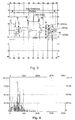
- a CMV (Vno) waveform and an associated CMC waveform are illustrated that result during one switching period when standard SVPWM control is employed.
- a dv/dt occurs which results in current spikes ands the peak to peak value of the CMV is Vdc.
- Fig. 4 shows an FFT spectrum plot of CMC corresponding to Fig. 3.
- Figs. 5 and 6 include plots similar to those shown in Figs. 3 and 4, respectively, albeit where DPWM was employed instead of SVPWM.
- modified modulators for diode rectifier/inverter systems have been developed that modify inverter switching patterns so that zero switching states (V0 and V7) are virtually (as opposed to actually) created by using two active vectors that are 180 degree out of phase. By virtually creating the zero switching states the peak-to-peak amplitude of the CMV can be significantly reduced.
- modified modulators are based on direct-digital SVPWM where dwell-times must be calculated in real-time for optimal performance.
- the CMV peak-to-peak amplitude generated by boost rectifier/inverter systems can be restricted to be no more than 1.33V dc by synchronizing the switching sequence between the rectifier and inverter stages of the system.
- Unfortunately synchronization of the switching sequences is not easy to facilitate when the switching frequency of the boost rectifier is different than the frequency of the inverter.
- Some modified modulators for active rectifier/inverter systems have been developed that can further reduce the number of CMV pulses in a three-phase system where synchronized switching is realized.
- this proposed method can reduce the total number of CMV pulses by one-third.
- At least some inventive embodiments include a method for reducing common mode noise in a three phase pulse width modulated (PWM) system that includes a three phase waveform generator that generates first, second and third modulating waveforms, a carrier signal generator and a PWM generator that compares modulating waveforms and the carrier signal to generate switch control signals for controlling at least one of converter and inverter switches, the method comprising the steps of receiving the first, second and third modulating waveforms, identifying one of the modulating waveforms that is at least one of instantaneously the maximum and instantaneously the minimum of the modulating waveforms as a first identified waveform, wherein comparison of the first identified waveform to the carrier signal would generate a first on-off pulse sequence associated with a phase corresponding to the first identified waveform, generating switch control signals associated with the phase corresponding to the first identified waveform that cause a modified on-off pulse sequence that is phase shifted from the first pulse sequence, using the second and third modulating waveforms to generate second and third on-off pulse sequences
- Other embodiments include a method for reducing common mode noise in a three phase pulse width modulated (PWM) system that includes positive and negative DC links, at least one of a converter and an inverter that includes first, second and third upper switching devices that link each of the first, second and third phases to the positive DC link and first, second and third lower switching devices that link each of the first, second and third phases to the negative DC link, respectively, a three phase waveform generator that generates first, second and third modulating waveforms, a carrier signal generator and a PWM generator that compares modulating waveforms and the carrier signal to generate switch control signals for controlling at least one of the converter and inverter switches, the switch control signals periodically commanding zero vectors V0 and V7 wherein each of the upper switches are on to link the three phases to the positive DC rail and where each of the lower switches are on to link the three phases to the negative DC rail, the method comprising the steps of receiving the first, second and third modulating waveforms, identifying the instantaneous maximum modulating waveforms as a
- Still other embodiments include a method for reducing common mode noise in a three phase pulse width modulated (PWM) system that includes positive and negative DC links, at least one of a converter and an inverter that includes first, second and third upper switching devices that link each of the first, second and third phases to the positive DC link and first, second and third lower switching devices that link each of the first, second and third phases to the negative DC link, respectively, a three phase waveform generator that generates first, second and third modulating waveforms, a carrier signal generator and a PWM generator that compares modulating waveforms and the carrier signal to generate switch control signals for controlling at least one of the converter and inverter switches, the switch control signals periodically commanding zero vectors V0 and V7 wherein each of the upper switches are on to link the three phases to the positive DC rail and where each of the lower switches are on to link the three phases to the negative DC rail, the method comprising the steps of receiving the first, second and third modulating waveforms, identifying the instantaneous minimum modulating waveforms as
- Some embodiments include an apparatus for reducing common mode noise in a three phase pulse width modulated (PWM) system that includes a three phase waveform generator that generates first, second and third modulating waveforms and at least one of a converter and an inverter, the apparatus comprising a processor programmed to receive the first, second and third modulating waveforms, identify one of the modulating waveforms that is at least one of instantaneously the maximum and instantaneously the minimum of the modulating waveforms as a first identified waveform, wherein comparison of the first identified waveform to the carrier signal would generate a first on-off pulse sequence associated with a phase corresponding to the first identified waveform, generate switch control signals associated with the phase corresponding to the first identified waveform that cause a modified on-off pulse sequence that is phase shifted from the first pulse sequence, use the second and third modulating waveforms to generate second and third on-off pulse sequences corresponding to the second and third phases and provide the modified pulse sequence and the second and third pulse sequences to the one of the inverter and
- Still other embodiments include an apparatus for reducing common mode noise in a three phase pulse width modulated (PWM) system that includes positive and negative DC links, at least one of a converter and an inverter that includes first, second and third upper switching devices that link each of the first, second and third phases to the positive DC link and first, second and third lower switching devices that link each of the first, second and third phases to the negative DC link, respectively, a three phase waveform generator that generates first, second and third modulating waveforms, a carrier signal generator and a PWM generator that compares modulating waveforms and the carrier signal to generate switch control signals for controlling at least one of the converter and inverter switches, the switch control signals periodically commanding zero vectors V0 and V7 wherein each of the upper switches are on to link the three phases to the positive DC rail and where each of the lower switches are on to link the three phases to the negative DC rail, the apparatus comprising a processor programmed to receive the first, second and third modulating waveforms, identify the instantaneous maximum modulating waveforms as
- Some embodiments include an apparatus for reducing common mode noise in a three phase pulse width modulated (PWM) system that includes positive and negative DC links, at least one of a converter and an inverter that includes first, second and third upper switching devices that link each of the first, second and third phases to the positive DC link and first, second and third lower switching devices that link each of the first, second and third phases to the negative DC link, respectively, a three phase waveform generator that generates first, second and third modulating waveforms, a carrier signal generator and a PWM generator that compares modulating waveforms and the carrier signal to generate switch control signals for controlling at least one of the converter and inverter switches, the switch control signals periodically commanding zero vectors V0 and V7 wherein each of the upper switches are on to link the three phases to the positive DC rail and where each of the lower switches are on to link the three phases to the negative DC rail, the apparatus comprising a processor programmed to receive the first, second and third modulating waveforms, identify the instantaneous minimum modulating waveforms as
- Still other embodiments include an apparatus for reducing common mode noise in a three phase pulse width modulated (PWM) system that includes at least one of a converter and an inverter that includes first, second and third upper switching devices and first, second and third lower switching devices, a three phase waveform generator that generates first, second and third modulating waveforms and a PWM generator that uses the modulating waveforms to generate switch control signals for controlling the upper and lower switches, the PWM system operating in a first sector when the first modulating waveform is maximum and the third modulating waveform is minimum, operating in a second sector when the second modulating waveform is maximum and the third modulating waveform is minimum, operating in a third sector when the second modulating waveform is maximum and the first modulating waveform is minimum, operating in a fourth sector when the third modulating waveform is maximum and the first modulating waveform is minimum, operating in a fourth sector when the third modulating waveform is maximum and the first modulating waveform is minimum, operating in a fifth sector when the third modulating waveform is maximum and the
- Fig. 1 is a schematic diagram of an exemplary rectifier/inverter system for feeding three-phase power to a motor load;
- Fig. 2 is a phase diagram illustrating various vectors and associated sectors corresponding to switch states for the switches of the inverter shown in Fig. 1;
- Fig. 3 is a graph illustrating a common mode voltage and a common mode current that result when conventional space vector PWM control is employed;
- Fig. 4 is a FFT plot corresponding to the current in Fig. 3;
- Fig. 5 is similar to Fig. 3, albeit corresponding to DPWM control;
- Fig. 6 is a FFT plot corresponding to the current in Fig. 5;
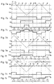
- Fig. 7a is a graph illustrating an exemplary carrier signal and three modulating waveforms
- Fig. 7b includes three pulse trains, a separate pulse train corresponding to each of the modulating waveforms in Fig. 7a;
- Fig. 7c illustrates a common mode voltage that results when the pulse trains of Fig. 7b are used to control the inverter of Fig. 1;
- Fig. 7d illustrates an exemplary carrier signal, two unmodified modulating waveforms and one modified modulating waveform that is consistent with at least one inventive embodiment
- Fig. 7e illustrates a pulse train that is associated with the modified modulating waveform of Fig. 7d;
- Fig. 7f illustrates a common mode voltage that results when the modified pulse train of Fig. 7e and two of the unmodified pulse trains of Fig. 7b are used to drive or control the inverter of Fig. 7;
- Fig. 7g is similar to Fig. 7d, albeit showing two unmodified modulating waveforms and one other modified modulating waveform;
- Fig. 7h is similar to Fig. 7e, albeit illustrating a pulse train corresponding to the modified modulating waveform of Fig. 7g;
- Fig. 7i is similar to Fig. 7f, albeit corresponding to two unmodified pulse trains of Fig. 7b and the modified pulse train of Fig. 7h;
- Fig. 8 is a flow chart illustrating one method for modifying modulating waveforms that is consistent with Figs. 7d-7f;
- Fig. 9 is a sub process that may be substituted for a portion of the process of Fig. 8 and that corresponds to Figs. 7g-7i;
- Figs 10a, 10b and 10c are identical to Figs. 7a, 7b and 7c, respectively;
- Fig. 10d is similar to Fig. 7d, albeit illustrating two unmodified modulating waveforms and one modified modulating waveform that is modified in a manner different than that in Fig. 7d;
- Fig. 10e illustrates a pulse sequence associated with the modified modulating waveform of Fig. 10d
- Fig. 10f illustrates the pulse sequence of Fig. 10e inverted
- Fig. 10g is similar to Fig. 7i, albeit illustrating a common mode voltage that results from using the pulse sequence of Fig. 10f and two unmodified pulse sequences of Fig. 10b to control the inverter of Fig. 1;
- Fig. 11 illustrates another exemplary method for modifying modulating waveforms that is consistent with the waveforms and pulse sequences of Figs. 10d - 10g;
- Fig. 12 is a schematic illustrating a circuit diagram that may be used to implement a portion of the method Fig. 11;
- Fig. 13 is a sub process that may be substituted for a portion of the method of Fig. 11 and that is consistent with yet another inventive method;
- Figs. 14a-14g are similar to Figs. 10a-10g, albeit corresponding to a method including a sub process shown in Fig. 13;
- Fig. 15 is a schematic illustrating processing components that may be employed to implement yet another inventive embodiment
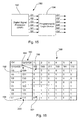
- Fig. 16 is a Karnaugh diagram related to the method of Fig. 8 that is used to generate an equation for a modified switch control signal G1' given different operating sectors and different instantaneous vectors;
- Fig. 17 is similar to Fig. 16, albeit for a switch control signal G3';
- Fig. 18 is similar to Fig. 16, albeit for a switch control signal G5';
- Figs. 19-21 are similar to Figs. 16-18, albeit showing information for developing equations to implement the subprocess of Fig. 9 instead of the process of Fig. 8;
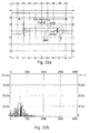
- Fig. 22a is a graph illustrating common mode voltage and common mode current akin to the graph shown in Fig. 3, albeit where one of the inventive methods has been employed to reduce common mode voltage and common mode current;
- Fig. 22b is similar to Fig. 4, albeit corresponding to the current illustrated in Fig. 22a;
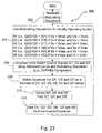
- Fig. 23 is a flow diagram illustrating another inventive method
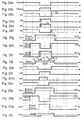
- Figs. 24a through 24r illustrate various switch control signals including ideal control signals for upper switches in two phases, corresponding control signals for upper switches in two phases and associated lower switches where turn on delays have been added, resulting phase voltages, a resulting common mode voltage, switch control signals for two phases where compensation for the turn on delays has been implemented, resulting phase voltages and a resulting common mode voltage for operation of a system during a subperiod of sector 1 operation when u and w phase currents are both positive;
- Figs. 25a through 25r are similar to Figs. 24a through 24r, albeit corresponding to sector 2 operation when only the u phase current is positive;
- Figs. 26a through 26r are similar to Figs. 24a through 24r, albeit corresponding to sector 1 operation when only the u phase current is positive;
- Figs. 27a through 27r are similar to Figs. 24a through 24r, albeit corresponding to sector 2 operation when both the u and v phase currents are positive;
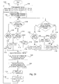
- Fig. 28 is a flowchart illustrating a method consistent with the method described above with respect to Fig. 8, albeit where dead time compensation is implemented;
- Fig. 29 is a subprocess that may be substituted for a portion of the method of Fig. 28 that is consistent with the method described above with respect to Fig. 9, albeit where dead time compensation is implemented;
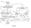
- Fig. 30 is a subprocess that may be substituted for a portion of the method of Fig. 28, albeit implementing yet another inventive method that results in reduced common mode voltage spikes, albeit where the number of dv/dts is not reduced;
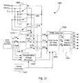
- Fig. 31 is a schematic illustrating a system for implementing at least some of the inventive methods described with respect to the other figures.
- the common mode noise reduction schemes described herein are to be used with carrier-based PWM control systems and do not require dwell-time calculations.
- the schemes can be applied to active rectifiers as well as PWM inverters to reduce common mode noise which includes both CMV and CMC.
- Each of the three schemes generates three phase switch control signals where the on-off duty cycles are identical to those generated via SVPWM, DPWM or some other conventional PWM control scheme but where the phase voltages are shifted or distributed differently so that common mode noise is reduced.
- the first and second schemes operate to alter modulating waveforms while the third scheme operates to modify switch control signals.
- the first, second and third noise reducing schemes will be referred to as a "max-min scheme", an “inverting scheme” and a “control signal modifying scheme” and will be described separately.
- FIG. 7 several graphs are used to illustrate carrier signals, three phase modulating waveforms, switch control signals that result from comparison of the carrier signals and modulating waveforms and resulting voltages Vno, Vno'. etc.
- Signal Tc is an exemplary high frequency carrier signal and Vur
- Vvr and Vwr are exemplary three phase modulating waveforms (only small segments of the modulating waveforms are shown so the waveforms appear to be horizontal line segments).
- Signals G1, G3 and G5 correspond to switches having the same labels in Fig. 1 and correspond to modulating waveforms Vur, Vvr and Vwr, respectively.
- a PWM generator when a PWM generator is set up to operate according to "active high" rules, when one of the modulating waveforms is above the carrier signal Tc, the corresponding switch signal is high and when the modulating waveform is below the carrier signal Tc the corresponding switch signal is low.
- signal G1 immediately prior to time t1, because waveform Vur is below signal Tc, signal G1 is low, between times t1 and t6, waveform Vur is above signal Tc and signal G1 is high, between times t6 and t7 waveform Vur is again below signal Tc and signal G1 is low, and so on.
- signal G3 is low and between times t2 and t5 and immediately after time t8 signal G3 is high
- signal G5 is low and between times t3 and t4, signal G5 is high.
- At least some PWM generators are also able to be set up to operate according to "active low” rules where a control signal is high when an associated modulating waveform is below a carrier signal Tc and the control signal is low when the associated modulating waveform is above the carrier signal.
- signals G1, G3 and G5 correspond to conventional drive operation and result in a common mode voltage component Vno as illustrated that includes six dv/dts per carrier cycle where a separate dv/dt occurs each time one of the modulating waveforms Vur, Vvr or Vwr intersects the carrier signal Tc (i.e., a separate dv/dt occurs at least of times t1, t2, t3, t4, t5 and t6 during the full carrier cycle illustrated in Fig. 7).
- a processor identifies the instantaneous maximum and minimum values of the three waveforms and alters one of the maximum and minimum modulating waveforms to generate a modified modulating waveform by either setting the maximum value equal to the minimum value or setting the minimum value equal to the maximum value. Thereafter, the PWM generator set up is changed for the phase corresponding to the modified modulating waveform only.
- the generator is set to operate according to active low rules for the phase corresponding to the modified modulating waveform and if the PWM generator was initially or is normally set up to operate according to active low rules, the generator is set to operate according to active high rules for the phase corresponding to the modified modulating waveform. For the two unmodified modulating waveforms the PWM generator set up is unchanged.
- the PWM generator compares the modulating waveform to the carrier signal Tc using the modified PWM generator set up rules and compares the other two unmodified modulating waveforms to the carrier signal Tc using the initial or original PWM generator set up rules and generates switch control signals that are used to drive the inverter.
- a first exemplary method 100 consistent with one embodiment of the max-min scheme is illustrated.
- the PWM generator rules are set to either active high or active low.
- the rules are set to active high.
- a drive processor identifies the maximum Vmax and minimum Vmin of the three phase voltages Vur, Vvr and Vwr.
- the instantaneous maximum and minimum voltages are Vur and Vwr, respectively, and therefore instantaneous operation of the system is in the first sector S1 (see again Fig. 2).
- the processor modifies one of the modulating waveforms by setting the maximum phase waveform equal to the minimum phase waveform.
- Vur is set equal to Vwr.
- Fig. 7d a modified waveform Vur' is illustrated just below waveform Vwr to indicate equality.
- PWM generator set up is modified for the u phase which corresponds to the modified modulating waveform Vur'.
- the set up for the u phase is modified so that the generator operates according to active low rules for the u phase.
- the modulating waveforms including the modified waveform Vur' and the unmodified waveforms Vvr and Vwr are provided to the PWM generator ands used to generate switch control signals.
- the resulting switch signals in the present example include signals G3 and G5 in Fig. 7b and modified switch signal G1' in Fig. 7e.
- signals G1', G3 and G5 and complimentary signals G2, G4 and G6 (not illustrated) are used to drive the inverter of Fig. 1, voltage Vno' illustrated in Fig. 7f results.
- voltage Vno' has only two dv/dts per carrier cycle and the peak value is less than in Fig. 7c and therefore CMC is substantially reduced.
- the average duty cycle (i.e., on to off durations) of the modified switch control signal G1' is identical to the average duty cycle of the original control signal G1, the only difference between the two signals G1 and G1' being that the on and off times have been shifted. More specifically, signal G1' has been shifted so that off periods align with on periods of signal G5 and therefore, as seen by comparing Figs. 7c and 7f, dv/dts at times t0, t1, t3, t4, t6, t7, etc., are eliminated so that the peak value of Vno' is reduced when compared to the peak value of Vno.
- a subprocess that may be used to replace step 106 in Fig. 8 is illustrated where, instead of replacing the maximum modulating waveform with the minimum, the minimum waveform is replaced with the maximum.
- control may pass to block 112 in Fig. 9.
- the instantaneous maximum and minimum voltages are Vur and Vwr, respectively.
- the processor modifies one of the modulating waveforms by setting the minimum phase waveform equal to the maximum phase waveform. For instance, referring again to Fig. 7a, because Vur is the maximum and Vwr is the minimum, at block 112, Vwr is set equal to Vur.
- Fig. 7g a modified waveform Vwr' is illustrated just above waveform Vur to indicate equality.
- the set up for the w phase is modified so that the generator operates according to active low rules for the w phase.
- the modulating waveforms including the modified waveform Vwr' and the unmodified waveforms Vur and Vvr are provided to the PWM generator ands used to generate switch control signals.
- the resulting switch signals in the present example include signals G1 and G3 in Fig. 7b and modified switch signal G5' in Fig. 7h.
- signals G1, G3 and G5' and complimentary signals G2, G4 and G6 (not illustrated) are used to drive the inverter of Fig. 1, voltage Vno' illustrated in Fig. 7i results.
- voltage Vno' has only two dv/dts per carrier cycle and the peak value is less than in Fig. 7c and therefore CMC is substantially reduced.
- the results using this second max-min method are identical to the results that occur when using the first method corresponding to Figs. 7e and 7f.
- FIG. 10 series of figures several graphs are used to illustrate carrier signals Tc, three phase modulating waveforms Vur, Vvr, Vwr, etc., switch control signals G1, G3, G5, etc., that result from comparison of the carrier signals and modulating waveforms and resulting voltages Vno, Vno'. etc., that are akin to similar signals and waveforms shown in the Fig. 7 series of figures.
- a PWM generator is set to operate according to active high rules so that when one of the modulating waveforms is above the carrier signal Tc, the corresponding switch signal is high and when the modulating waveform is below the carrier signal Tc the corresponding switch signal is low.
- signals G1, G3 and G5 correspond to conventional drive operation and result in a common mode voltage component Vno as illustrated that includes six dv/dts per carrier cycle where a separate dv/dt occurs each time one of the modulating waveforms Vur, Vvr or Vwr intersects the carrier signal Tc (i.e., a separate dv/dt occurs at least of times t1, t2, t3, t4, t5 and t6 during the full carrier cycle illustrated in Fig. 7).
- a processor identifies the instantaneous maximum (or, in the alternative, instantaneous minimum) value of the three waveforms and generates three separate invert control signals, one for each of the waveforms, where the invert control signal corresponding to the maximum (or, in the alternative, minimum) is high and the other two invert control signals are low.
- hardware circuits like the circuit illustrated in Fig. 12 are provided for each of the three phases and each hardware circuit receives an associated modulating waveform and corresponding invert control signal.
- the hardware circuit that receives the high invert control signal causes the associated modulating waveform to be inverted and the inverted signal is then compared to the carrier signal Tc to generate an intermediate switch control signal.
- the other two non-inverted modulating waveforms are also compared to the carrier signal Tc to generate switch control signals for the other two phases.
- the intermediate switch signal is inverted to generate a modified switch signal and then the modified switch signal and the two unmodified switch signals are used to drive the inverter of Fig. 1.
- a first exemplary method 120 consistent with one embodiment of the inverting scheme is illustrated.
- the PWM generator rules are set to active high (or, in at least some embodiments, active low).
- a drive processor identifies the maximum Vmax of the three phase voltages Vur, Vvr and Vwr.
- the instantaneous maximum voltage is Vur.
- the processor modifies one of the modulating waveforms by inverting the maximum phase modulating waveform. For instance, referring again to Fig. 10a, because Vur is the maximum, at block 126, Vur is set equal to -Vur. In Fig. 10d, a modified waveform -Vur is illustrated just below waveform Vwr.
- the modulating waveforms including the modified waveform -Vur and the unmodified waveforms Vvr and Vwr are provided to the PWM generator and used to generate switch control signals.
- the resulting switch signals in the present example include signals G3 and G5 in Fig. 10b and intermediate switch signal G1 i in Fig. 10e. Intermediate signal G1 i is then inverted to generate negated modified signal G1' as shown in Fig. 10f.
- signals G1', G3 and G5 and complimentary signals G2, G4 and G6 (not illustrated) are used to drive the inverter of Fig. 1, voltage Vno' illustrated in Fig. 10g results. As shown, voltage Vno' has only two dv/dts per carrier cycle and the peak value is less than in Fig. 10c and therefore CMC is substantially reduced.
- a hardware circuit 150 for the u-phase includes two switches 154 and 160, an inverter 152, a comparator 156 and a negator 158.
- the input on line 162 is the u phase modulating waveform
- the input on line 164 is the invert control signal for the u phase that indicates if the phase is maximum (or, in the alternative, minimum)
- the input on line 166 is a carrier signal Tc.
- Waveform Vur is provided to inverter 152 and to one input of switch 154.
- the output of inverter 152 is provided to the second input of switch 154.
- the invert control signal is provided to the control input of switch 154 and selects Vur as an output when Vur is not the maximum value (or, in the alternative, is not the minimum value) and selects -Vur as the output when Vur is the maximum value (or, in the alternative, is the minimum value).
- the output of switch 154 is provided to comparator 156 along with carrier signal Tc and the output of comparator 156 is provided as one input to switch 160 and to negator 158.
- the output of negator 158 is provided as the second input to switch 160.
- the invert control signal is also provided to the control input of switch 160.
- a subprocess 138 that may be used to replace steps 124 and 126 in Fig. 11 is illustrated where, instead of inverting the maximum modulating waveform, the minimum waveform is inverted and the resulting control signal is negated prior to inverter control.
- Figs. 14a - 14c are identical to Figs. 10a through 10c described above and are only repeated here to simplify this explanation.
- control may pass to block 140 in Fig. 13.
- the instantaneous minimum voltage is Vwr.
- the processor modifies one of the modulating waveforms by inverting the minimum phase waveform.
- Vwr is the minimum
- Vwr' is set equal to -Vwr.
- a modified waveform -Vwr is illustrated just above waveform Vur.
- the resulting switch signals in the present example include signals G1 and G3 in Fig. 14b and intermediate switch signal G5i in Fig. 14e. Intermediate signal G5i is then inverted to generate negated modified signal G5' as shown in Fig. 14f.
- signals G1, G3 and G5' and complimentary signals G2, G4 and G6 (not illustrated) are used to drive the inverter of Fig. 1, voltage Vno' illustrated in Fig. 14g results. As shown, voltage Vno' has only two dv/dts per carrier cycle and the peak value is less than in Fig. 14c and therefore CMC is substantially reduced.
- the inverting method shifts the switch control signals of one phase so that the pulses of one phase cancel the pulses of a second phase which in turn reduces the number of dv/dts in Vno' and which also reduces the peak values of Vno'.
- a configuration 180 includes a digital signal processor (DSP) 182 and a programmable logic device (PLD) 184.
- DSP digital signal processor
- PLD programmable logic device
- the output signals of processor 182 are provided to PLD 184 which generates six modified control signals G1', G2', G3' G4', G5' and G6' where signals G2', G4' and G6' are the inverse of signals G1', G3' and G5', respectively.
- the general idea is to develop logic that can perform the same function as the methods described above so that the end result is identical to the results shown in Fig. 7b for G3 and G5, Fig. 7e for G1' and Fig. 7f for Vno' during sector S1 operation and similar results during operation in the other sectors S2 through S6.
- Karnaugh diagrams have been formed as illustrated in Figs. 16 through 18 for modified switch control signals G1' through G36', respectively, that correspond to the method illustrated in Fig. 8 (i.e., the max-min scheme where the maximum modulating waveform is replaced by the minimum modulating waveform).
- the exemplary Karnaugh diagram 188 includes a G1 G3G5 column 186 indicating values for each of switches G1, G3 and G5 generated by DSP 182 where the G1G3G5 combination corresponds to one of the eight possible vectors (e.g., V0 through V7 as illustrated in Fig. 2).
- Diagram 188 also includes sector columns S1 through S6 that correspond to similarly labeled sectors in Fig. 2 and that are each associated with a different Q2Q1Q0 combination. For instance, sector S1 corresponds to the Q2Q1Q0 combination "001”, sector S3 corresponds to the Q2Q1Q0 combination "011”, and so on.
- signals G3 and G5 remain unchanged while signal G1 is altered to generate signal G1' by changing the signal G1 from off to on when the G1 G3G5 combination is 000 (i.e., when vector V0 occurs) and by changing signal G1 from on to off when combination G1 G3G5 is 111 (i.e., when vector V7 occurs).
- signal G1 is altered to generate signal G1' by changing the signal G1 from off to on when the G1 G3G5 combination is 000 (i.e., when vector V0 occurs) and by changing signal G1 from on to off when combination G1 G3G5 is 111 (i.e., when vector V7 occurs).
- changes made to signal G1 to generate signal G1' during sector S6 are identical to the changes that are made during sector S1 (i.e., when vectors V0 and V7 occur, G1 is changed from 0 to 1 and from 1 to 0, respectively, to generate signal G1').
- signal G1' is equal to the original signal G1 because the waveform Vur associated with signal G1 is not the maximum among waveforms Vur, Vvr and Vwr.
- signals G3' and G5' are identical to signals G3 and G5 which is consistent with the information presented in the Fig. 7 series of figures. More specifically, in Fig. 17, signal G3' is 0, 0, 1, 1, 0, 0, 1, 1 during vectors V0 through V7, respectively, and in Fig. 18, signal G5' is 0, 1, 0, 1, 0, 1, 0, 1 during vectors V0 through V7, respectively.
- the waveform Vvr associated with signal G3 is the maximum among waveforms Vur, Vvr and Vwr and therefore signal G3' is altered to eliminate occurrence of vectors V0 and V7 while each of signals G1' and G5' remain unchanged from the original G1 and G5 values (see signals G1' and G5' during sectors S2 and S3 in Figs. 16 and 18, respectively).
- signal G3 is changed from 0 to 1 and from 1 to 0 when vectors V0 and V7 occur, respectively.
- the waveform Vwr associated with signal G5 is the maximum among waveforms Vur, Vvr and Vwr and therefore signal G5' is altered to eliminate occurrence of vectors V0 and V7 while each of signals G1' and G3' remain unchanged from the original G1 and G3 values (see signals G1' and G3' during sectors S4 and S5 in Figs. 16 and 17, respectively).
- signal G5 is changed from 0 to 1 and from 1 to 0 when vectors V0 and V7 occur, respectively.
- PLD 184 is programmed to solve Equations 5 through 7 based on inputs G1, G2 and G3 as well as values Q0, Q1 and Q2.
- Signals G2', G4' and G6' are the inverse of related signals G1', G3' and G5'.
- Signals G1', G2', G3', G4', G5' and G6' are used to drive the switches of the inverter or converter controlled thereby.
- G 3 ⁇ G 1 ⁇ ⁇ G 3 + G 1 ⁇ G 3 ⁇ G 5 ⁇ + G 1 ⁇ ⁇ G 3 ⁇ ⁇ G 5 ⁇ + G 1 ⁇ ⁇ G 3 ⁇ ⁇ G 5 ⁇ ⁇ Q 2 ⁇ Q 1 ⁇ ⁇ Q 0 + Q 2 ⁇ Q 1 ⁇ ⁇ Q 0 + G 1 ⁇ G 3 ⁇
- PLD 184 is programmed to solve Equations 8 through 10 based on inputs G1, G2 and G3 as well as values Q0, Q1 and Q2.
- Signals G2', G4' and G6' are the inverse of related signals G1', G3' and G5'.
- Signals G1', G2', G3', G4', G5' and G6' are used to drive the switches of the inverter or converter controlled thereby.
- an exemplary method 200 for implementing the signal modifying scheme is shown.
- modulating waveforms Vu, Vv and Vw are generated.
- the modulating waveforms are used to identify the instantaneous sector (e.g., S1, S2, etc.) of operation according to the illustrated rules so that Q2, A1 and Q0 values can be determined.
- DSP 182 (see Fig. 15) generates signals G1, G2 and G3 and provides values Q2, Q1 and Q0 to PLD.
- PLD 184 solves either equations 5-7 or equations 8-10 to generate modified switching signals G1', G3' and G5'.
- signals G2, G4' and G6' are derived from signals G1', G3' and G5', respectively and at block 212 signals G1' through G6' are used to drive the inverter or converter to be controlled thereby.
- Figs. 22a and 22b plots similar to those shown in Figs. 3 and 4 are shown where one of the inventive methods described above was employed to modify SVPWM control to reduce CMV and CMC. Comparing Figs. 22a and 22b to 3 and 4 it can be seen that using one of the inventive methods, the magnitude of the peak to peak swing in the CMV is one third the magnitude when standard SVPWM is employed. In addition, it can be seen that the number of dv/dts during a switching cycle are reduced appreciably (i.e., from six to two) which in turn reduces CMC spiking. In fact, experiments have shown that the RMS CMC is reduced from 1.0 pu to 0.577 pu using the inventive schemes to modify SVPWM control.
- the results where the present invention is used to reduce CMV and CMC in the context of DPWM control are also positive.
- the number of dv/dts during a switching cycle are reduced from four to two, the peak to peak CMV is reduced by half and experiments have shown that the RMS CMC is reduced from 0.816 pu to 0.577 pu using the inventive schemes to modify DPWM control.
- Fig. 24 series of figures a number of graphs illustrate voltage Vno dips that occur during a sub-period of sector S1 (see again Fig. 2) operation when dead time compensation as well known in the PWM control arts is applied to switch control signals after the Max-Min scheme as described above has been applied.
- the sub-period of sector S1 represented by the Fig. 24 series of figures corresponds to the sub-period when phase currents iu and iw are positive.
- Figs. 24 series of figures corresponds to the sub-period when phase currents iu and iw are positive.
- ideal G1 ideal and G5ideal switch control signals are illustrated that result from setting an initial maximum reference waveform Vur equal to the minimum reference waveform signal Vwr and altering PWM control (e.g., resetting the generator from active high to active low for the modified reference phase waveform) in a manner consistent with the method described above with respect to the Fig. 7 series of figures.
- Dead time compensation is also applied to the third phase (i.e., affecting signals G3 and G4) but the affect there does not cause Vno dips during operation in this specific sub-period of sector S1 operation because signal G3 is not aligned with either of signals G1 or G5 and therefore the compensation does not combine with one of the other phases to cause a Vno dip.
- Figs. 24c and 24e illustrate G1 and G5 signals after dead time compensation has been implemented to delay the G1 and G5 turn on times from times t4 to t5 and from times t1 to t2, respectively, resulting in delays Td as illustrated.
- Figs. 24d and 24f show how the turn on times of signals G2 and G6 associated with signals G1 and G5 have been delayed. Referring to Figs. 24g, 24h and 24i, resulting phase voltages Vuo, Vvo and Vwo are shown and in Fig.
- a resulting Vno waveform is illustrated which includes multiple dv/dts at times t0, t1, t2, t3, t4 and t6 and reduced Vno dips that occur between times t1 and t2 and times t3 and t4.
- dead time compensation is implemented after the Max-Min scheme has been implemented, six dv/dts occur during each carrier signal half cycle.
- the Fig. 25 series includes figures akin to the Fig. 24 series of figures during the sub-period of sector S2 operation when only current iu is positive.
- ideal signals G3 ideal and G5 ideal and related signals are illustrated that correspond to the maximum and minimum reference voltages Vvr and Vwr, respectively.
- dead time compensation results in turn on delays Td illustrated in Figs. 25c - 25f and voltages Vuo, Vvo and Vwo (see Figs. 25g - 25i) which in turn cause voltage Vno (see Fig.
- the number of dv/dts that occur during sector S1 and sector S2 operation can be reduced by modifying either the modulating or reference waveforms prior to comparison to the carrier signal by the PWM inverter or by modifying the switch control signals generated by the PWM generator.
- the turn on times of each of signals G1' and G5' are simply advanced from times t5 and t2 to times t4 and t1, respectively, and signals G2' and G6' are modified accordingly as illustrated in Figs. 24l and 24n.
- modified voltage Vno' does not include the four dv/dts at times t1, t2, t3 and t4 that occurred in Fig. 24j.
- turn on times of signal G1 can be advanced and turn off times of signal G5 can be advanced by a turn on period Td to eliminate the voltage spikes as best seen in Fig. 25r.
- FIG. 26 series of figures figures akin to the figures illustrated in the Fig. 24 series of figures are shown, albeit corresponding to operation during the sub-period of sector 1 operation that occurs when only current iu is positive (i.e., currents iv and iw are each negative).
- voltage Vno results in the pulse form in Fig. 26j after dead time compensation has occurred where voltage Vno does not include either spikes or dips.
- turn on times and turn off times are advanced for phases that have positive and negative currents in a manner consistent with the description above with respect to the Fig. 24 and Fig. 25 series of figures, respectively, the resulting voltage Vno' is unchanged.
- FIG. 27 series of figures figures akin to the figures illustrated in the Fig. 24 series of figures are shown, albeit corresponding to operation during the sub-period of sector 2 operation that occurs when only current iw is negative (i.e., currents iu and iv are each positive).
- voltage Vno results in Fig. 27j after dead time compensation has occurred where voltage Vno does not include either spikes or dips.
- turn on times and turn off times are advanced for phases that have positive and negative currents in a manner consistent with the description above with respect to the Fig. 24 and Fig. 25 series of figures, respectively, the resulting voltage Vno' is unchanged.
- One way to advance turn on or turn off times is to alter a modulating waveform.
- a PWM generator is operated in the active high mode of operation (i.e., a switch control signal goes high (i.e., to 1) when the reference signal is greater than the carrier signal) and a phase current is positive
- the turn on time of a switch control signal generated by comparing the reference signal to a carrier signal can be advanced by increasing the reference signal by a compensation voltage value Vcom where Vcom is a value that is selected to compensate for the effects of dead time compensation plus, in at least some embodiments, to compensate for device dynamics and/or other parasitic losses.
- the turn off time of a switch control signal generated by comparing the reference signal to a carrier signal can be advanced by decreasing the reference signal by a compensation voltage value Vcom.
- the turn on time of a switch control signal generated by comparing the reference signal to a carrier signal can be advanced by decreasing the reference signal by a compensation voltage value Vcom where Vcom is a value that is selected to compensate for the effects of dead time compensation plus, in at least some embodiments, to compensate for device dynamics and/or other parasitic losses.
- the turn off time of a switch control signal generated by comparing the reference signal to a carrier signal can be advanced by increasing the reference signal by a compensation voltage value Vcom.
- Table 3 below summarizes how modulating or reference waveforms are to be modified to eliminate the dead time related spikes and dips described above where modifications in box 1, box 2, box 7 and box 8 correspond to compensation that occurs during active low operation and modifications in box 3, bos 4, box 5 and box 6 correspond to compensation that occurs during active high operation.
- Table 3 Carrier status Counting up Counting down Motor current polarity iL>0 iL ⁇ 0 iL>0 iL ⁇ 0 Trigger pulse: (Box 1) (Box 2) (Box 3) (Box 4) Turn on -Vcom 0 +Vcom 0 Trigger pulse: (Box 5) (Box 6) (Box 7) (Box 8) Turn off 0 -Vcom 0 +Vcom
- a method 1100 for modifying modulating waveforms in a manner consistent with the method described above with respect to Fig. 8 where dead time compensation is also facilitated is illustrated.
- the PWM generator is set up to be either active high or active low.
- the PWM generator is initially set up to operate according to an active high protocol.
- a processor determines the maximum, medium and minimum reference voltages among the three phases of the system. After block 1104, control passes to each of blocks 1106 and 1130.
- a processor determines whether or not the maximum current Imax is greater than zero where the maximum current is associated with the maximum phase voltage Vmax. Where the maximum current is greater than zero, control passes to block 1108 where the processor determines whether or not the carrier signal is counting up or counting down. Where the carrier signal is counting up, control passes to block 1112 where the maximum reference voltage Vmax is set equal to the minimum voltage reference Vmin minus the compensation voltage Vcom after which control passes to block 1120. Referring again to decision block 1108, where the carrier status is counting down, control passes to block 1114 where the maximum reference voltage Vmax is set equal to the minimum reference voltage Vmin after which control passes to block 1120.
- the processor determines whether or not the carrier status is counting up or down. Where the carrier is counting up, control passes to block 1114 where maximum reference voltage Vmax is set equal to the minimum reference voltage Vmin after which control passes to block 1120. Referring again to decision block 1110, where the carrier is counting down, control passes to block 1116 where the maximum reference voltage Vmax is set equal to minimum reference voltage Vmin plus the compensation voltage value Vcom after which control passes to block 1120.
- the processor determines whether or not the minimum phase current Imin is greater than zero where the minimum phase current is associated with the minimum phase reference voltage Vmin. Similarly, at block 1130, the processor determines whether or not the medium phase current Imed is greater than zero where the medium phase current is associated with the medium phase reference voltage Vmed. Where one or both of the minimum or medium phase currents is less than zero or negative, control passes to block 1132 where the processor determines whether or not the carrier is counting up or down. Where the carrier is counting down, control passes to block 1134 where the reference voltage associated with the negative minimum and/or medium phase current is modified by subtracting the compensation voltage value Vcom after which control passes to block 1120. At block 1132, where the carrier is counting up, control passes to block 1138 where the phase reference voltage associated with the negative maximum or medium phase current is unchanged after which control passes to block 1120.
- control passes to block 1136 where the processor determines whether or not the carrier is counting up or down. Where the carrier is counting up at block 1136, control passes to block 1140 where the compensation voltage Vcom is added to the phase reference voltage associated with the positive phase current at block 1130 after which control passes to block 1120.
- the reference voltage modifications that take place at blocks 1106, 1008, 1110, 1112, 1114 and 1116 correspond to modifications to the maximum reference voltage Vmax and are consistent with the modifications in Table 3 corresponding to box 1, box 2, box 7 and box 8.
- the modification that occurs at block 1112 corresponds to mod1 where the current is positive and the carrier status is counting up
- the modification that occurs at block 1116 corresponds to box 8 where the current is negative and the carrier status is counting down
- block 1114 corresponds to box 2 and box 7 where the current is negative and the carrier is counting up and the current is positive and the carrier is counting down, respectively.
- modifications to the reference voltages that occur at blocks 1130, 1132, 1134, 1136,1138 and 1140 modify the minimum and medium reference voltages Vmin and Vmed and correspond to modifications to Table 3 including box 3, box 4, box 5 and box 6.
- the modifications that occur at block 1140 correspond to box 3
- the modifications (or lack thereof) at block 1138 correspond to box 4 and box 5
- the modifications at block 1134 correspond to box 6 in Table 3.
- the processor modifies the PWM generator set up so that, instead of being set active high, the generator is set up for active low for the phase associated with the maximum reference voltage Vmax.
- the PWM generator compares the carrier signal to the modulating waveforms to generate the modified control signals.
- dead time compensation delays are used to modify the control signals and at block 1126 control signals compensated for dead time are used to control the inverter. After block 1126, control passes back up to block 1104 where the process continues.
- a subprocess 1200 that may be substituted for a portion of the process illustrated in Fig. 28 is shown, albeit where modulating waveform modifications are consistent with the subprocess shown in Fig. 9 instead of the process shown in Fig. 8.
- control may pass to both of blocks 1206 and 1230 in Fig. 29.
- the subprocess shown is akin to the subprocess in Fig. 28 that occurs between blocks 1104 and 1120 where the minimum phase current Imin and the minimum phase reference voltage Vmin are swapped for the maximum phase current Imax and the maximum phase reference voltage Vmax in all of the blocks.
- Block 1206 in Fig. 29 is akin to block 1106 in Fig. 28, block 1208 in Fig. 29 is akin to block 1108 in Fig. 28, block 1234 in Fig. 29 is akin to block 1134 in Fig. 28, and so on.
- block 1206 in Fig. 29 is akin to block 1106 in Fig. 28
- block 1208 in Fig. 29 is akin to block 1108 in Fig.
- block 1234 in Fig. 29 is akin to block 1134 in Fig. 28, and so on.
- the primary differences between the process associated with Figs. 28 and 29 is that, in Fig. 28 maximum reference voltages are replaced by minimum reference voltages and in Fig. 29 minimum reference voltages are replaced by maximum reference voltages.
- Fig. 30 one additional sub process 1300 that may be substituted for a portion of the process in Fig. 28 is illustrated for modifying modulating waveforms in a manner that reduces the magnitude of spikes in voltage Vno that occur as a result of conventional dead time compensation.
- the subprocess of Fig. 30 instead of altering just one of the maximum and minimum phase reference voltages as in Figs. 28 and 29, both the maximum and minimum phase reference voltages are modified.
- control may pass to each of blocks 1306 and 1330 in Fig. 30.
- a processor determines whether or not the maximum phase current Imax is positive or negative where the maximum phase current is associated with the maximum phase reference voltage Vmax.
- the processor determines whether or not the minimum phase current Imin is positive or negative where the minimum phase current is associated with the minimum phase reference voltage Vmin. Where any one of the minimum or maximum phase currents is positive, control passes to block 1308 where the processor determines whether or not the carrier is counting up or down. Where the carrier is counting up, control passes to block 1312 where the phase reference voltages associated with positive current at block 1306 are modified. Specifically, where the maximum phase current Imax was positive at block 1306, the maximum phase reference voltage Vmax is set equal to the minimum phase reference voltage Vmin minus the compensation voltage Vcom. Similarly, where the minimum phase current Imin was positive at block 1306, the minimum phase reference voltage Vmin is set equal to the maximum phase reference voltage Vmax minus the compensation voltage Vcom.
- the processor determines whether or not the carrier is counting up or down. Where the carrier is counting up, control passes to block 1314 where, for each of the maximum and minimum phase reference currents associated with a negative phase current at block 1306, the phase reference voltage is set equal to the other of the maximum and minimum phase reference voltages after which control passes to block 1120 in Fig. 28. Where the carrier is counting down at block 1310, control passes to block 1316 where, for each of the maximum and minimum phase reference voltages associated with a negative current at block 1306, the processor sets the phase reference voltage equal to the other of the maximum and minimum phase reference voltages plus the compensation voltage Vcom. After block 1316, control passes to block 1120 in Fig. 28.
- the processor determines whether or not the medium phase current Imed which is associated with the medium phase reference voltage Vmed is positive or negative. Where the medium phase current Imed is negative, control passes to block 1332 where the processor checks carrier status. Where the carrier is counting up at block 1332, control passes to block 1334 where the medium reference voltage Vmed is decremented by compensation voltage Vcom after which control passes to block 1120. At block 1332, where the carrier is counting down, control passes to block 1338 where the medium reference voltage Vmed is not changed after which control passes to block 1120. At block 1330, where the medium phase current Imed is positive, control passes to block 1336 where carrier count is checked.
- System 1400 includes a carrier generator 1402, a compensation voltage processor 1404, three switching devices 1406, 1408 and 1410, a reference voltage modulator 1412, three summers 1414, 1416 and 1418 and a PWM generator 1420.
- reference voltage modulator 1412 generates three phase reference voltages Vur, Vvr and Vwr that are provided to summers 1414, 1416 and 1418, respectively.
- each of the reference voltages Vur, Vvr and Vwr are provided to compensation voltage processor 1404.
- the reference voltages Vur, Vvr and Vwr correspond to reference voltages that have already been modified to reduce the number of dv/dts that occur during each carrier cycle.
- a maximum reference voltage may have already been set equal to the minimum reference voltage.
- carrier generator 1402 generates a carrier signal that is typically a high frequency triangle type carrier signal.
- the carrier signal is provided to compensation voltage processor 1404 as well as to PWM generator 1420.
- Each of switching devices 1406, 1408 and 1410 is similarly constructed and operates in a similar fashion and therefore, in the interest of simplifying this explanation, only device 1406 will be described here in detail.
- Device 1406 is a three input and single output switch where the inputs include compensation voltage values Vcom and - Vcom as well as a zero input. Switch 1406 is controlled by compensation voltage processor 1404 whereby one of the three inputs Vcom, -Vcom and zero is selected as an output for the switch 1406.
- switches 1406, 1408 and 1410 are provided to summers 1414, 1416 and 1418, respectively.
- Summers 1414, 1416 and 1418 add or sum their inputs and provide compensated phase reference voltages Vurc, Vvrc and Vwrc, respectively, to generator 1420.
- generator 1420 includes a duty cycle - on time converter 1422 and a PWM signal module 1424.
- Converter 1422 receives the compensated reference voltages and the carrier signal and uses those signals to generate three switch control signals G1, G3 and G5 which are provided to signal module 1424.
- signals G1, G3 and G5 are provided to signal module 1424.
- Signal module 1424 uses the control signals G1, G3 and G5 to generate all six switch control signals G1 through G6 as illustrated.
- signals G1 through G6 are provided to a dead time compensator prior to driving an inverter or the like.
- processor 1404 controls the other components shown to perform one of the processes described above with respect to Figs. 28, 29 or 30.
- the output of the converter 1422 may be modified by simply shifting on and off times as appropriate in a manner consistent with that described above with respect to Table 3.
- the inventions is directed to a method and apparatus for reducing common mode noise in a three phase pulse width modulated (PWM) system, the method comprising the steps of receiving the first, second and third modulating waveforms, identifying one of the modulating waveforms that is at least one of instantaneously the maximum and instantaneously the minimum of the modulating waveforms as a first identified waveform, wherein comparison of the first identified waveform to the carrier signal would generate a first on-off pulse sequence associated with a phase corresponding to the first identified waveform, generating switch control signals associated with the phase corresponding to the first identified waveform that cause a modified on-off pulse sequence that is phase shifted from the first pulse sequence, using the second and third modulating waveforms to generate second and third on-off pulse sequences corresponding to the second and third phases and providing the modified pulse sequence and the second and third pulse sequences to the one of the inverter and
- PWM pulse width modulated
Landscapes
- Engineering & Computer Science (AREA)
- Power Engineering (AREA)
- Physics & Mathematics (AREA)
- Electromagnetism (AREA)
- Inverter Devices (AREA)
Applications Claiming Priority (1)
| Application Number | Priority Date | Filing Date | Title |
|---|---|---|---|
| US11/435,651 US7649756B2 (en) | 2006-05-17 | 2006-05-17 | Common mode noise reduction in converter systems through modification of single phase switching signal |
Publications (3)
| Publication Number | Publication Date |
|---|---|
| EP1858150A2 true EP1858150A2 (fr) | 2007-11-21 |
| EP1858150A3 EP1858150A3 (fr) | 2011-08-31 |
| EP1858150B1 EP1858150B1 (fr) | 2017-10-18 |
Family
ID=38456550
Family Applications (1)
| Application Number | Title | Priority Date | Filing Date |
|---|---|---|---|
| EP07009825.6A Ceased EP1858150B1 (fr) | 2006-05-17 | 2007-05-16 | Procédés de modulation et appareil de réduction du bruit en mode commun |
Country Status (2)
| Country | Link |
|---|---|
| US (1) | US7649756B2 (fr) |
| EP (1) | EP1858150B1 (fr) |
Cited By (11)
| Publication number | Priority date | Publication date | Assignee | Title |
|---|---|---|---|---|
| CN101295935B (zh) * | 2007-12-10 | 2010-06-02 | 西北工业大学 | 一种可抑制谐波的优化pwm调制方法 |
| CN101997473A (zh) * | 2009-08-20 | 2011-03-30 | 上海御能动力科技有限公司 | 伺服控制器的降噪控制方法 |
| CN102185339A (zh) * | 2011-05-13 | 2011-09-14 | 中国电子科技集团公司第三十六研究所 | 一种三相光伏并网空间矢量调制序列的选择方法 |
| CN102857137A (zh) * | 2012-08-24 | 2013-01-02 | 江苏兆伏新能源有限公司 | 逆变器调制方法及其用途 |
| CN102882462A (zh) * | 2012-09-21 | 2013-01-16 | 联合汽车电子有限公司 | 组合式svpwm调制方法 |
| CN103715956A (zh) * | 2013-12-16 | 2014-04-09 | 华南理工大学 | 一种二电平三相空间矢量脉冲宽度调制器及其svpwm优化方法 |
| EP2207259A3 (fr) * | 2009-01-07 | 2016-07-13 | Rockwell Automation Technologies, Inc. | Systèmes et procédés pour la réduction de la tension en mode commun dans des entraînements CA |
| US9716444B2 (en) | 2015-11-05 | 2017-07-25 | Ge Energy Power Conversion Technology Ltd | Pulse width modulation (PWM) for multi-level power inverters |
| EP2395652A3 (fr) * | 2010-04-16 | 2017-08-09 | Rockwell Automation Inc. | Systèmes et procédés pour réduire les courants en mode commun d'un entraînement CA |
| EP2487785B1 (fr) * | 2011-02-09 | 2019-01-02 | Rockwell Automation Technologies, Inc. | Convertisseur de puissance avec réduction de tension de mode commun |
| CN109495004A (zh) * | 2018-12-14 | 2019-03-19 | 合肥工业大学 | 奇数相三电平变流器的非连续脉宽调制方法 |
Families Citing this family (30)
| Publication number | Priority date | Publication date | Assignee | Title |
|---|---|---|---|---|
| US7518335B2 (en) * | 2006-08-04 | 2009-04-14 | Gm Global Technology Operations, Inc. | Method and apparatus for PWM control of voltage source inverter to minimize current sampling errors in electric drives |
| JP4301336B2 (ja) * | 2007-10-24 | 2009-07-22 | ダイキン工業株式会社 | 電力変換装置 |
| US8319466B2 (en) | 2011-02-21 | 2012-11-27 | Rockwell Automation Technologies, Inc. | Modular line-to-ground fault identification |
| FR2973181B1 (fr) * | 2011-03-21 | 2014-05-16 | Hispano Suiza Sa | Procede de commande simplifie d'un convertisseur de tension alternative triphasee en tension continue |
| US8570003B2 (en) | 2011-04-13 | 2013-10-29 | Rockwell Automation Technologies, Inc. | Double fed induction generator converter and method for suppressing transient in deactivation of crowbar circuit for grid fault ridethrough |
| JP5304937B2 (ja) * | 2011-09-30 | 2013-10-02 | ダイキン工業株式会社 | 電力変換装置 |
| DE102011118044A1 (de) * | 2011-11-09 | 2013-05-16 | Conti Temic Microelectronic Gmbh | Verfahren zur Steuerung eines Motors mittels Pulsweitenmodulation (PWM) |
| US9041234B2 (en) | 2012-03-26 | 2015-05-26 | Rockwell Automation Technologies, Inc. | Double fed induction generator (DFIG) converter and method for improved grid fault ridethrough |
| KR101993379B1 (ko) | 2012-09-11 | 2019-06-26 | 삼성전자주식회사 | 전동기를 구동하는 인버터의 출력전압을 제어하는 방법 및 장치. |
| CN103684001B (zh) * | 2012-09-17 | 2016-05-11 | 苏州三星电子有限公司 | 变频空调中功率开关的控制方法及装置 |
| JP5900470B2 (ja) * | 2013-11-28 | 2016-04-06 | 株式会社安川電機 | 電流形電力変換装置 |
| US9236828B1 (en) | 2014-07-03 | 2016-01-12 | Rockwell Automation Technologies, Inc. | Methods and power conversion system control apparatus to control IGBT junction temperature at low speed |
| US9318976B1 (en) | 2014-10-30 | 2016-04-19 | Rockwell Automation Technologies, Inc. | Adjustable PWM method to increase low speed starting torque and inverter voltage measurement accuracy |
| CN105391325B (zh) * | 2015-12-17 | 2017-12-08 | 艾思玛新能源技术(上海)有限公司苏州高新区分公司 | 一种基于空间电压矢量脉宽调制的调制方法 |
| US9602041B1 (en) * | 2016-01-08 | 2017-03-21 | Newfrey Llc | Software-controlled electronic circuit for switching power to a three-phase motor |
| CN105634255B (zh) * | 2016-01-29 | 2018-01-30 | 浙江大学宁波理工学院 | 一种基于18脉冲的svpwm三相电子调压器 |
| US9847733B2 (en) | 2016-05-12 | 2017-12-19 | Rockwell Automation Technologies, Inc. | Power conversion system with DC bus regulation for abnormal grid condition ride through |
| CN106452128B (zh) * | 2016-10-31 | 2019-01-22 | 许继电源有限公司 | 解决空间矢量脉宽调制电流过零点畸变的控制方法和装置 |
| US10381968B2 (en) | 2017-12-05 | 2019-08-13 | Otis Elevator Company | Converter pulse width modulation strategies for three phase regenerative drives |
| US10250161B1 (en) | 2018-04-05 | 2019-04-02 | Rockwell Automation Technologies, Inc. | Adaptive harmonic elimination compensation for voltage distortion elements |
| CN108712064B (zh) * | 2018-06-28 | 2019-11-05 | 郑州轻工业学院 | 一种电压源逆变器模型预测的共模电压抑制方法 |
| CN110011581B (zh) * | 2019-01-28 | 2020-11-24 | 华中科技大学 | 一种非对称六相交流电机共模噪声的抑制方法和系统 |
| US10784797B1 (en) | 2019-06-19 | 2020-09-22 | Rockwell Automation Technologies, Inc. | Bootstrap charging by PWM control |
| CN110380670B (zh) * | 2019-07-20 | 2021-06-08 | 哈尔滨工业大学 | 能够消除奇次pwm频率谐波的空间矢量脉宽调制方法 |
| CN110768605B (zh) * | 2019-10-30 | 2021-09-07 | 中国第一汽车股份有限公司 | 一种svpwm调制方法、装置及系统 |
| CN112838773A (zh) * | 2019-11-25 | 2021-05-25 | 开利公司 | 具有不对称半导体额定值布置的功率模块和转换器 |
| US11031897B1 (en) | 2020-01-24 | 2021-06-08 | Rockwell Automation Technologies, Inc. | Method and apparatus for mitigation of DC bus pump-up |
| CN111711223B (zh) * | 2020-05-13 | 2023-08-04 | 许昌开普检测研究院股份有限公司 | 提高光伏逆变器效率和谐波性能的混合空间矢量调制方法 |
| US11336206B2 (en) | 2020-09-23 | 2022-05-17 | Rockwell Automation Technoligies, Inc. | Switching frequency and PWM control to extend power converter lifetime |
| CN118381298A (zh) * | 2024-05-10 | 2024-07-23 | 深圳威迈斯新能源(集团)股份有限公司 | 一种相移不连续脉宽调制方法及三相变换器 |
Family Cites Families (17)
| Publication number | Priority date | Publication date | Assignee | Title |
|---|---|---|---|---|
| US5625550A (en) * | 1994-09-27 | 1997-04-29 | Allen-Bradley Company, Inc. | Apparatus used with AC motors for compensating for turn on delay errors |
| US6005362A (en) * | 1998-02-13 | 1999-12-21 | The Texas A&M University Systems | Method and system for ride-through of an adjustable speed drive for voltage sags and short-term power interruption |
| US6031738A (en) * | 1998-06-16 | 2000-02-29 | Wisconsin Alumni Research Foundation | DC bus voltage balancing and control in multilevel inverters |
| KR100318171B1 (ko) * | 1998-11-17 | 2002-04-22 | 설승기 | 3상펄스폭변조컨버터-인버터시스템에서의커먼-모드전압펄스제거방법 |
| WO2001020351A1 (fr) * | 1999-09-17 | 2001-03-22 | Delphi Technologies, Inc. | Procede economique servant a mesurer la position rotative haute resolution de machines electriques |
| US6600669B2 (en) * | 2001-06-27 | 2003-07-29 | The Board Of Regents Of The University And Community College System Of Nevada, On Behalf Of The University Of Nevada At Reno | Random pulse width modulation method and device |
| US6469916B1 (en) * | 2001-10-01 | 2002-10-22 | Rockwell Automation Technologies, Inc. | Method and apparatus for compensating for device dynamics and voltage drop in inverter based control systems |
| US6477067B1 (en) * | 2001-10-02 | 2002-11-05 | Rockwell Automation Technologies, Inc. | Method and apparatus for compensating for device dynamics in inverter based control systems |
| DE10156694B4 (de) * | 2001-11-17 | 2005-10-13 | Semikron Elektronik Gmbh & Co. Kg | Schaltungsanordnung |
| EP1555743A1 (fr) * | 2002-04-15 | 2005-07-20 | Jialin Wu | Convertisseur de puissance polyvalent |
| US6819078B2 (en) * | 2002-10-15 | 2004-11-16 | International Rectifier Corporation | Space vector PWM modulator for permanent magnet motor drive |
| KR100488529B1 (ko) * | 2003-05-20 | 2005-05-11 | 삼성전자주식회사 | 3상모터구동용 인버터의 제어장치 및 제어방법 |
| FI115265B (fi) * | 2003-08-28 | 2005-03-31 | Vacon Oyj | Taajuusmuuttajan pulssinleveysmodulointi |
| FI121491B (fi) * | 2004-11-11 | 2010-11-30 | Vacon Oyj | Taajuusmuuttajan ylijännitesuojaus |
| US7075267B1 (en) * | 2004-12-29 | 2006-07-11 | Prolific Technology Inc. | Space vector-based current controlled PWM inverter for motor drives |
| US7274576B1 (en) * | 2006-03-01 | 2007-09-25 | Rockwell Automation Technologies, Inc. | Power converter with reduced common mode voltage |
| US7639518B2 (en) * | 2006-04-26 | 2009-12-29 | Nissan Motor Co., Ltd. | Device and method for controlling power converting device |
-
2006
- 2006-05-17 US US11/435,651 patent/US7649756B2/en active Active
-
2007
- 2007-05-16 EP EP07009825.6A patent/EP1858150B1/fr not_active Ceased
Non-Patent Citations (1)
| Title |
|---|
| None |
Cited By (15)
| Publication number | Priority date | Publication date | Assignee | Title |
|---|---|---|---|---|
| CN101295935B (zh) * | 2007-12-10 | 2010-06-02 | 西北工业大学 | 一种可抑制谐波的优化pwm调制方法 |
| EP2207259A3 (fr) * | 2009-01-07 | 2016-07-13 | Rockwell Automation Technologies, Inc. | Systèmes et procédés pour la réduction de la tension en mode commun dans des entraînements CA |
| CN101997473A (zh) * | 2009-08-20 | 2011-03-30 | 上海御能动力科技有限公司 | 伺服控制器的降噪控制方法 |
| CN101997473B (zh) * | 2009-08-20 | 2013-12-25 | 上海御能动力科技有限公司 | 伺服控制器的降噪控制方法 |
| EP2395652A3 (fr) * | 2010-04-16 | 2017-08-09 | Rockwell Automation Inc. | Systèmes et procédés pour réduire les courants en mode commun d'un entraînement CA |
| EP2487785B1 (fr) * | 2011-02-09 | 2019-01-02 | Rockwell Automation Technologies, Inc. | Convertisseur de puissance avec réduction de tension de mode commun |
| CN102185339A (zh) * | 2011-05-13 | 2011-09-14 | 中国电子科技集团公司第三十六研究所 | 一种三相光伏并网空间矢量调制序列的选择方法 |
| CN102185339B (zh) * | 2011-05-13 | 2013-11-20 | 中国电子科技集团公司第三十六研究所 | 一种三相光伏并网空间矢量调制序列的选择方法 |
| CN102857137A (zh) * | 2012-08-24 | 2013-01-02 | 江苏兆伏新能源有限公司 | 逆变器调制方法及其用途 |
| CN102857137B (zh) * | 2012-08-24 | 2016-01-20 | 艾思玛新能源技术(上海)有限公司 | 逆变器调制方法及其用途 |
| CN102882462A (zh) * | 2012-09-21 | 2013-01-16 | 联合汽车电子有限公司 | 组合式svpwm调制方法 |
| CN103715956B (zh) * | 2013-12-16 | 2015-12-02 | 华南理工大学 | 一种二电平三相空间矢量脉冲宽度调制器及其svpwm优化方法 |
| CN103715956A (zh) * | 2013-12-16 | 2014-04-09 | 华南理工大学 | 一种二电平三相空间矢量脉冲宽度调制器及其svpwm优化方法 |
| US9716444B2 (en) | 2015-11-05 | 2017-07-25 | Ge Energy Power Conversion Technology Ltd | Pulse width modulation (PWM) for multi-level power inverters |
| CN109495004A (zh) * | 2018-12-14 | 2019-03-19 | 合肥工业大学 | 奇数相三电平变流器的非连续脉宽调制方法 |
Also Published As
| Publication number | Publication date |
|---|---|
| US7649756B2 (en) | 2010-01-19 |
| EP1858150B1 (fr) | 2017-10-18 |
| US20070268051A1 (en) | 2007-11-22 |
| EP1858150A3 (fr) | 2011-08-31 |
Similar Documents
| Publication | Publication Date | Title |
|---|---|---|
| EP1858150A2 (fr) | Procédés de modulation et appareil de réduction du bruit en mode commun | |
| EP1860762A2 (fr) | Procédés de modulation et appareil de réduction du bruit en mode commun | |
| US7106025B1 (en) | Cancellation of dead time effects for reducing common mode voltages | |
| Kwak et al. | Model predictive control methods to reduce common-mode voltage for three-phase voltage source inverters | |
| US6023417A (en) | Generalized discontinuous pulse width modulator | |
| US9007789B2 (en) | Electric circuit for high voltage power conversion | |
| EP3682538B1 (fr) | Control à base de modulation de largeur d'impulsion pour un convertisseur multiniveaux | |
| US7206211B2 (en) | Converter and a method for controlling a converter | |
| US20100164418A1 (en) | Power Converting Apparatus | |
| Lee et al. | An improved phase-shifted PWM method for a three-phase cascaded H-bridge multi-level inverter | |
| Vu et al. | Model-predictive current control scheme for seven-phase voltage-source inverter with reduced common-mode voltage and current harmonics | |
| US8947897B2 (en) | Current-source power converting apparatus | |
| HU226738B1 (en) | Method for processing pwm waves | |
| Jahmeerbacus et al. | Evaluation of Selective Harmonic Elimination and sinusoidal PWM for single-phase DC to AC inverters under dead-time distortion | |
| Bharatiraja et al. | FPGA based design and validation of asymmetrical reduced switch multilevel inverter | |
| WO2018179234A1 (fr) | Convertisseur en pont h et conditionneur d'énergie | |
| JP7494321B2 (ja) | 三相3レベルインバータの駆動制御装置および駆動制御方法 | |
| Baranwal et al. | A modified four-step commutation to suppress common-mode voltage during commutations in open-end winding matrix converter drives | |
| Jacob et al. | Space vector pulse width modulation for a seven level inverter applied to an induction motor drive | |
| Fischer et al. | Investigation on carrier signals to minimize the overall current ripple of an interleaved-switched inverter | |
| Furukawa et al. | Optimal pulse pattern determination based on Pulse Harmonic Modulation | |
| Kumar et al. | Implementation of Single Phase Cascaded H-Bridge Nine Level Inverter and Simulation Study with PI Controller | |
| Cha et al. | An approach to reduce common mode voltage in matrix converter | |
| EP1860761B1 (fr) | Dispositif et méthode de contrôle d'onduleurs connectés en série | |
| Dixon et al. | Traction Drive System for Electric Vehicles, Using Multilevel Converters |
Legal Events
| Date | Code | Title | Description |
|---|---|---|---|
| PUAI | Public reference made under article 153(3) epc to a published international application that has entered the european phase |
Free format text: ORIGINAL CODE: 0009012 |
|
| AK | Designated contracting states |
Kind code of ref document: A2 Designated state(s): AT BE BG CH CY CZ DE DK EE ES FI FR GB GR HU IE IS IT LI LT LU LV MC MT NL PL PT RO SE SI SK TR |
|
| AX | Request for extension of the european patent |
Extension state: AL BA HR MK YU |
|
| PUAL | Search report despatched |
Free format text: ORIGINAL CODE: 0009013 |
|
| AK | Designated contracting states |
Kind code of ref document: A3 Designated state(s): AT BE BG CH CY CZ DE DK EE ES FI FR GB GR HU IE IS IT LI LT LU LV MC MT NL PL PT RO SE SI SK TR |
|
| AX | Request for extension of the european patent |
Extension state: AL BA HR MK RS |
|
| RIC1 | Information provided on ipc code assigned before grant |
Ipc: H02M 7/5387 20070101AFI20110727BHEP Ipc: H02M 7/53 20060101ALI20110727BHEP Ipc: H02M 1/44 20070101ALI20110727BHEP Ipc: H02M 5/458 20060101ALI20110727BHEP |
|
| 17P | Request for examination filed |
Effective date: 20120228 |
|
| AKX | Designation fees paid |
Designated state(s): DE FR GB |
|
| REG | Reference to a national code |
Ref country code: DE Ref legal event code: R079 Ref document number: 602007052711 Country of ref document: DE Free format text: PREVIOUS MAIN CLASS: H02M0007538700 Ipc: H02M0001120000 |
|
| RIC1 | Information provided on ipc code assigned before grant |
Ipc: H02M 5/458 20060101ALI20170427BHEP Ipc: H02M 1/12 20060101AFI20170427BHEP Ipc: H02M 7/5387 20070101ALI20170427BHEP Ipc: H02M 1/44 20070101ALI20170427BHEP |
|
| GRAP | Despatch of communication of intention to grant a patent |
Free format text: ORIGINAL CODE: EPIDOSNIGR1 |
|
| INTG | Intention to grant announced |
Effective date: 20170616 |
|
| GRAS | Grant fee paid |
Free format text: ORIGINAL CODE: EPIDOSNIGR3 |
|
| GRAA | (expected) grant |
Free format text: ORIGINAL CODE: 0009210 |
|
| AK | Designated contracting states |
Kind code of ref document: B1 Designated state(s): DE FR GB |
|
| REG | Reference to a national code |
Ref country code: GB Ref legal event code: FG4D |
|
| REG | Reference to a national code |
Ref country code: DE Ref legal event code: R096 Ref document number: 602007052711 Country of ref document: DE |
|
| REG | Reference to a national code |
Ref country code: FR Ref legal event code: PLFP Year of fee payment: 12 |
|
| REG | Reference to a national code |
Ref country code: DE Ref legal event code: R097 Ref document number: 602007052711 Country of ref document: DE |
|
| PLBE | No opposition filed within time limit |
Free format text: ORIGINAL CODE: 0009261 |
|
| STAA | Information on the status of an ep patent application or granted ep patent |
Free format text: STATUS: NO OPPOSITION FILED WITHIN TIME LIMIT |
|
| 26N | No opposition filed |
Effective date: 20180719 |
|
| PGFP | Annual fee paid to national office [announced via postgrant information from national office to epo] |
Ref country code: FR Payment date: 20200422 Year of fee payment: 14 Ref country code: DE Payment date: 20200421 Year of fee payment: 14 |
|
| PGFP | Annual fee paid to national office [announced via postgrant information from national office to epo] |
Ref country code: GB Payment date: 20200423 Year of fee payment: 14 |
|
| REG | Reference to a national code |
Ref country code: DE Ref legal event code: R119 Ref document number: 602007052711 Country of ref document: DE |
|
| GBPC | Gb: european patent ceased through non-payment of renewal fee |
Effective date: 20210516 |
|
| PG25 | Lapsed in a contracting state [announced via postgrant information from national office to epo] |
Ref country code: GB Free format text: LAPSE BECAUSE OF NON-PAYMENT OF DUE FEES Effective date: 20210516 Ref country code: DE Free format text: LAPSE BECAUSE OF NON-PAYMENT OF DUE FEES Effective date: 20211201 |
|
| PG25 | Lapsed in a contracting state [announced via postgrant information from national office to epo] |
Ref country code: FR Free format text: LAPSE BECAUSE OF NON-PAYMENT OF DUE FEES Effective date: 20210531 |