EP1860700A2 - Verfahren zur Behandlung einer gerieften Oberfläche, insbesondere einer Glasplatte eines Halbleiterwafers - Google Patents
Verfahren zur Behandlung einer gerieften Oberfläche, insbesondere einer Glasplatte eines Halbleiterwafers Download PDFInfo
- Publication number
- EP1860700A2 EP1860700A2 EP07009759A EP07009759A EP1860700A2 EP 1860700 A2 EP1860700 A2 EP 1860700A2 EP 07009759 A EP07009759 A EP 07009759A EP 07009759 A EP07009759 A EP 07009759A EP 1860700 A2 EP1860700 A2 EP 1860700A2
- Authority
- EP
- European Patent Office
- Prior art keywords
- wafer
- transparent material
- plate
- layer
- polymeric material
- Prior art date
- Legal status (The legal status is an assumption and is not a legal conclusion. Google has not performed a legal analysis and makes no representation as to the accuracy of the status listed.)
- Withdrawn
Links
Images


Classifications
-
- C—CHEMISTRY; METALLURGY
- C03—GLASS; MINERAL OR SLAG WOOL
- C03C—CHEMICAL COMPOSITION OF GLASSES, GLAZES OR VITREOUS ENAMELS; SURFACE TREATMENT OF GLASS; SURFACE TREATMENT OF FIBRES OR FILAMENTS MADE FROM GLASS, MINERALS OR SLAGS; JOINING GLASS TO GLASS OR OTHER MATERIALS
- C03C17/00—Surface treatment of glass, not in the form of fibres or filaments, by coating
- C03C17/28—Surface treatment of glass, not in the form of fibres or filaments, by coating with organic material
- C03C17/32—Surface treatment of glass, not in the form of fibres or filaments, by coating with organic material with synthetic or natural resins
-
- H—ELECTRICITY
- H10—SEMICONDUCTOR DEVICES; ELECTRIC SOLID-STATE DEVICES NOT OTHERWISE PROVIDED FOR
- H10F—INORGANIC SEMICONDUCTOR DEVICES SENSITIVE TO INFRARED RADIATION, LIGHT, ELECTROMAGNETIC RADIATION OF SHORTER WAVELENGTH OR CORPUSCULAR RADIATION
- H10F39/00—Integrated devices, or assemblies of multiple devices, comprising at least one element covered by group H10F30/00, e.g. radiation detectors comprising photodiode arrays
- H10F39/011—Manufacture or treatment of image sensors covered by group H10F39/12
- H10F39/026—Wafer-level processing
-
- H—ELECTRICITY
- H10—SEMICONDUCTOR DEVICES; ELECTRIC SOLID-STATE DEVICES NOT OTHERWISE PROVIDED FOR
- H10F—INORGANIC SEMICONDUCTOR DEVICES SENSITIVE TO INFRARED RADIATION, LIGHT, ELECTROMAGNETIC RADIATION OF SHORTER WAVELENGTH OR CORPUSCULAR RADIATION
- H10F39/00—Integrated devices, or assemblies of multiple devices, comprising at least one element covered by group H10F30/00, e.g. radiation detectors comprising photodiode arrays
- H10F39/80—Constructional details of image sensors
- H10F39/804—Containers or encapsulations
-
- H—ELECTRICITY
- H10—SEMICONDUCTOR DEVICES; ELECTRIC SOLID-STATE DEVICES NOT OTHERWISE PROVIDED FOR
- H10F—INORGANIC SEMICONDUCTOR DEVICES SENSITIVE TO INFRARED RADIATION, LIGHT, ELECTROMAGNETIC RADIATION OF SHORTER WAVELENGTH OR CORPUSCULAR RADIATION
- H10F39/00—Integrated devices, or assemblies of multiple devices, comprising at least one element covered by group H10F30/00, e.g. radiation detectors comprising photodiode arrays
- H10F39/80—Constructional details of image sensors
- H10F39/805—Coatings
- H10F39/8053—Colour filters
-
- H—ELECTRICITY
- H10—SEMICONDUCTOR DEVICES; ELECTRIC SOLID-STATE DEVICES NOT OTHERWISE PROVIDED FOR
- H10F—INORGANIC SEMICONDUCTOR DEVICES SENSITIVE TO INFRARED RADIATION, LIGHT, ELECTROMAGNETIC RADIATION OF SHORTER WAVELENGTH OR CORPUSCULAR RADIATION
- H10F39/00—Integrated devices, or assemblies of multiple devices, comprising at least one element covered by group H10F30/00, e.g. radiation detectors comprising photodiode arrays
- H10F39/80—Constructional details of image sensors
- H10F39/806—Optical elements or arrangements associated with the image sensors
- H10F39/8063—Microlenses
Definitions
- the present invention relates to the treatment of a striped surface and in particular the treatment of a glass surface covering a semiconductor wafer comprising CMOS imagers.
- CMOS imagers made using CMOS technology are currently the subject of an increasing number of applications because of their low cost compared to the imagers CCD (Charge Coupled Device).
- CCD Charge Coupled Device
- Such CMOS imagers were initially used to produce low resolution and poor quality image sensors (eg web cameras).
- CMOS imagers can compete with CCD imagers.
- the present invention is part of an effort to develop and perfect this imaging technology aimed at lowering cost prices at equal quality.
- FIG. 1 represents an exemplary image capture and / or video capture module using a CMOS imager, intended for example to be mounted in a portable device such as a mobile phone, a camera or a video camera.
- Module 1 comprises a frame 2, an optical block 3, lenses 4 integral with the block 3, an infrared filter 5 and a support 6.
- a semiconductor chip 100 incorporating a CMOS imager 10 is disposed on the support 6 and receives light passing through the lenses and the infrared filter.
- the CMOS imager 10 comprises photosites each forming a pixel (not visible in FIG. 1). Each pixel comprises a photodiode and a circuit for controlling and interconnecting the photodiode. The pixels are arranged in a matrix manner and a mosaic of red, green, blue filters is distributed over the pixel array, generally according to the Bayer architecture.
- Figure 2 is a schematic sectional view of the chip 100 and the CMOS imager 10 in a region corresponding to three pixels PIX1, PIX2, PIX3.
- a semiconductor substrate 15 in which the imager 10 is implanted, and a glass wafer 20 fixed to the imager via a layer of adhesive 19, for example an epoxy, urethane, silicone layer. ...
- the imager 10 comprises layers 10-1, 10-2, 10-3, 10-4, 10-5 and microlenses L0 (L0-1, L0-2, L0-3 ).
- Layer 10-1 represents the active part of the imager and includes photodiodes and their associated control and interconnection circuits (not detailed).
- the layer 10-2 is a dielectric material which completely covers the substrate 15.
- the layer 10-3 is a passivation layer deposited on the imager at the end of the manufacturing process.
- the layer 10-4 is formed by colored resins and comprises R, G, B areas of red, green or blue color forming the above-mentioned primary color filters, at the rate of one color-per-pixel filter.
- the layer 10-5 is a layer of intermediate resin forming a support for the microlenses L0 and offering good flatness (layer of "planarization”).
- the microlenses L0 are arranged in an "MLA” (Microlens Array) matrix at the rate of one microlens per pixel, and are covered by the adhesive layer 19 and by the glass plate 20.
- Steps of a method of manufacturing the chip 100 are shown in Figures 3A-3C.
- the method firstly comprises the collective fabrication of a plurality of imagers 10 i on a silicon wafer 15 ', as shown in FIG. 3A.
- a large glass plate 20 ' is fixed on the front face of the wafer by means of an adhesive layer 19' covering the entire wafer.
- the wafer 15 ' is reversed and is placed upside down on the glass plate 20', its front face facing upwards, to effect a treatment of its back side.
- This rear-end treatment comprises at least one step of thinning the wafer by mechanical abrasion (backlapping) of its rear face and a step of sawing the wafer to obtain a plurality of imaging chips such as the chip 100.
- the treatment in front the back can also include pre-cutting furrow formation, formation of conductive pads, formation of conductive beads (bumps), etc.
- the present invention thus aims at an alternative to this conventional solution.
- the present invention aims in particular a method for preventing the deposition and removal of a protective layer on the glass plate of a wafer.
- the present invention is based on an approach of the technical problem to be solved which is in a way the antithesis of the solution that we want to avoid: instead of preventing the appearance of scratches by systematically depositing a protective layer on each wafer in production, the present invention proposes to repair a damaged wafer by depositing a repair layer on its striped glass plate. Indeed, not all wafers are systematically damaged during the manufacturing process and only a small number of wafers is concerned. Under these conditions, it is cheaper to repair a striped wafer than to ensure that no wafer is scratched.
- the invention proposes to erase the scratches of a wafer by clogging, depositing on the scratched surface a repairing polymer layer having the same optical index as the striped glass. This solution is simple to implement and does not require a long and expensive operation as would be for example a scratch erasure polishing step.
- the present invention thus provides a method of treating a striped surface to pass electromagnetic radiation, comprising a deposition step on the scratched surface of at least one layer of a polymer material having substantially the same optical index as the material constituting the striped surface, way to seal the scratches, and a polymerization step of the polymeric material.
- the striped surface is made of glass.
- the layer of polymer material is deposited by centrifugal coating.
- the polymeric material is selected from the group consisting of photosensitive or planarizing resins and glues.
- the striped surface is made of a transparent material covering a semiconductor wafer.
- the invention also relates to a method for manufacturing semiconductor chips, each comprising a component implanted in the semiconductor, the method comprising a step of collectively implanting components on a front face of a semiconductor wafer, a step of fixing a plate of a transparent material on the front face of the wafer, wafer processing steps after mounting the transparent material plate, a wafer cutting step in individual chips and, after the steps of processing the wafer and before cutting it into chips, a step of depositing at least one layer of a polymer material on the outer face of the transparent material plate, the polymer material having substantially the same optical index as the transparent material.
- the transparent material is glass.
- the method comprises a step of controlling the outer face of the plate of transparent material, and the step of depositing the layer of polymer material is conducted only if the outer face the plate of transparent material has scratches.
- the wafer processing steps after mounting the transparent material plate comprise a step of thinning the wafer by abrasion of its rear face.
- the wafer processing steps after mounting the transparent material plate comprise steps of handling the wafer by means of automated machines.
- the step of implanting components on one side of the wafer comprises implanting imagers intended to capture images via the transparent material plate.
- the polymeric material is selected from the group consisting of photosensitive or planarizing resins and glues.
- the polymeric material is an adhesive used to fix the plate of transparent material on the front face of the wafer.
- the invention also relates to an imager implanted on a semiconductor chip, comprising a wafer of transparent material integral with the semiconductor chip through which the imager receives images to be captured, the outer face of the semiconductor chip.
- microplate of transparent material being covered with at least one layer of a polymeric material having substantially the same optical index as the transparent material.
- the chip of transparent material is made of glass.
- the polymeric material belongs to the group comprising photosensitive or planarizing resins and glues.
- the invention also relates to a portable device comprising a photographic module equipped with an imager according to the invention.
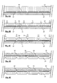
- FIG. 4A is identical to FIG. 3C and shows the previously described wafer 15 'on which a plurality of imagers 10i has been implanted, the front face of the wafer being covered by the glass plate 20' fixed by means of the layer glue 19 '.
- the wafer is placed upside down on a work surface (not shown) to carry out processing steps illustrated in FIGS. 4B and 4C.
- the step represented in FIG. 4B consists of a grinding and polishing (backlapping) of the rear face of the wafer in order to reduce its thickness, initially of the order of a few hundred micrometers and of the order of a few tens or a hundred micrometers at the end of the process.
- the step shown in FIG. 4C consists in practicing grooves or grooves on the rear face of the wafer. These grooves may be provided for various reasons, for example to facilitate the subsequent cutting of the wafer or to make contacts on the rear face.
- the grooves 25 are generally made by chemical etching or plasma etching.
- no protective layer is deposited on the outer face of the glass plate 20 ', which is therefore exposed to a risk of scratching during the step of FIG. 4B or during the step of the FIG. 4C, or even during handling steps occurring before or after each of these steps.
- a visual inspection of the wafer is carried out at the end of the step of FIG. 4C, or after a step of wafer handling occurring after the step of FIG. 4C, before the wafer is sawn to obtain imaging chips.
- a restorative layer of curable polymer material having substantially the same optical index as the glass is deposited on the glass plate to erase the scratches.
- the deposit is preferably carried out by spin coating.
- the deposited material may be liquid or gelatinous. It is then polymerized according to the required conditions (UV polymerization or thermal polymerization).
- a small amount of polymer material 30, of the order of a few milliliters, is deposited on the glass plate 20 ', preferably in the center of the wafer.
- the material 30 is spread over the entire surface of the glass plate 20 'by centrifugation.
- the speed of rotation of the wafer is quite low, for example 1500 rpm.
- a strong acceleration, for example up to 20000 rpm is then applied to the wafer to promote the formation of a uniform layer 31 'over the entire surface of the glass plate while eliminating the excess of polymeric material.
- the rotation speed is then stabilized at a lower value, for example of the order of 2000 to 7000 rpm, in order to define the thickness of the layer of spread polymer material.
- the rotation is still maintained for some time to allow the evaporation of the solvent.
- the evaporation of the solvent substantially reduces the viscosity of the polymer material which directly depends on the thickness of the film. Evaporation is fast, it is necessary to ensure that the spreading time of the polymer material is short.
- most of the solvent in the material evaporates to produce a solid film.
- a cooking step is conducted after the centrifugation step. This step ensures the rapid removal of the residual solvents and the polymerization of the restorative layer 31 'and is a function of the material used. This results in a contraction (volume shrinkage) of the polymer material, which causes a loss of thickness of the order of the fraction of a percent to a few percent, depending on the material used.
- the wafer is for example heated by means of hot plates brought to a temperature of the order of a hundred to a few hundred degrees (100-300 ° C. in general).
- the duration of the heating cycle is adjusted to reach the desired level of solvent, and may be from a few minutes to more than one hour.
- the cooking is followed by a step of cooling the wafer, for example by means of plates at room temperature.
- the polymerization step may also be conducted by exposing the wafer to UV radiation.
- the UV polymerization is generally shorter than the thermal polymerization and lasts only a few minutes at most.
- the invention can be implemented with any type of polymer material that can be deposited in liquid form and then cured, in particular the photosensitive resins (for example the "CT” resins used for the manufacture of microlenses of imagers), "planarizing” resins (used to form flat surfaces in microelectronics), color resins, etc. Tests within the reach of those skilled in the art allow to select the most appropriate materials depending on the nature and optical properties of the glass used.
- the photosensitive resins for example the "CT” resins used for the manufacture of microlenses of imagers
- planearizing resins used to form flat surfaces in microelectronics
- color resins etc. Tests within the reach of those skilled in the art allow to select the most appropriate materials depending on the nature and optical properties of the glass used.
- Adhesives can also be used, and generally any adhesive that can be polymerized in the presence of UV radiation or in the presence of heat.
- the material is chosen according to its optical characteristics and must have substantially the same optical index as the striped material to neutralize the appearance of an interface diopter where the scratches are.
- the material used to repair the scratches is identical to that used to glue the glass plate onto the wafer.
- the adhesive marketed under the reference OGR150THTG by the company Ablestick is an example of glue that can be used for this purpose.
- a same equipment allows both to drive the gluing step of the glass plate and the scratch repair step. The cost of implementing the method according to the invention is then minimal.
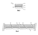
- an imaging chip 101 according to the invention obtained by cutting the wafer, is distinguished from the conventional chip 100 represented in FIG. 2 by the presence of a repairing layer 31 on the external face of its wafer. glass plate 20.
- At least one second restorative layer 32 ' can be deposited on the wafer after deposition of the first restorative layer 31'.
- the method according to the invention is applicable to all active or passive optical devices and in particular to digital image sensors embedded in portable devices comprising a photographic module of the type shown in FIG. 1, in particular mobile phones, cameras and cameras. video.
- the method according to the invention has been described in the foregoing in connection with the manufacture of a semiconductor wafer comprising a glass plate, the invention is applicable to any transparent material, in particular plexiglass , likely to replace the glass.
- the method according to the invention is also applicable to the treatment of all types of scratched surfaces intended to let electromagnetic radiation pass, either in the visible as in the example described above, either in the infrared or in the ultraviolet (or beyond), including filtering surfaces allowing only electromagnetic radiation having certain wavelengths to pass through.
Landscapes
- Chemical & Material Sciences (AREA)
- Life Sciences & Earth Sciences (AREA)
- Engineering & Computer Science (AREA)
- Chemical Kinetics & Catalysis (AREA)
- General Chemical & Material Sciences (AREA)
- Geochemistry & Mineralogy (AREA)
- Materials Engineering (AREA)
- Organic Chemistry (AREA)
- Solid State Image Pick-Up Elements (AREA)
- Treatments Of Macromolecular Shaped Articles (AREA)
Applications Claiming Priority (1)
| Application Number | Priority Date | Filing Date | Title |
|---|---|---|---|
| FR0604770A FR2901638A1 (fr) | 2006-05-26 | 2006-05-26 | Procede de traitement d'une surface rayee, notamment une plaque de verre d'un wafer de semi-conducteur |
Publications (2)
| Publication Number | Publication Date |
|---|---|
| EP1860700A2 true EP1860700A2 (de) | 2007-11-28 |
| EP1860700A3 EP1860700A3 (de) | 2008-03-12 |
Family
ID=37575137
Family Applications (1)
| Application Number | Title | Priority Date | Filing Date |
|---|---|---|---|
| EP07009759A Withdrawn EP1860700A3 (de) | 2006-05-26 | 2007-05-16 | Verfahren zur Behandlung einer gerieften Oberfläche, insbesondere einer Glasplatte eines Halbleiterwafers |
Country Status (3)
| Country | Link |
|---|---|
| US (1) | US20070290244A1 (de) |
| EP (1) | EP1860700A3 (de) |
| FR (1) | FR2901638A1 (de) |
Citations (1)
| Publication number | Priority date | Publication date | Assignee | Title |
|---|---|---|---|---|
| GB1262526A (en) | 1969-03-21 | 1972-02-02 | Minnesota Mining & Mfg | Coating for optical element |
Family Cites Families (4)
| Publication number | Priority date | Publication date | Assignee | Title |
|---|---|---|---|---|
| JPH02311331A (ja) * | 1989-05-26 | 1990-12-26 | Nippon Telegr & Teleph Corp <Ntt> | 光学ガラス表面傷の修復方法 |
| US6564018B2 (en) * | 1996-09-09 | 2003-05-13 | Creoscitek Corporation Ltd. | Imaging device for digital photography |
| JP2000235351A (ja) * | 1998-12-18 | 2000-08-29 | Hitachi Ltd | 画像表示装置及びその修正方法並びに修正装置 |
| US6482669B1 (en) * | 2001-05-30 | 2002-11-19 | Taiwan Semiconductor Manufacturing Company | Colors only process to reduce package yield loss |
-
2006
- 2006-05-26 FR FR0604770A patent/FR2901638A1/fr active Pending
-
2007
- 2007-05-16 EP EP07009759A patent/EP1860700A3/de not_active Withdrawn
- 2007-05-24 US US11/753,264 patent/US20070290244A1/en not_active Abandoned
Patent Citations (1)
| Publication number | Priority date | Publication date | Assignee | Title |
|---|---|---|---|---|
| GB1262526A (en) | 1969-03-21 | 1972-02-02 | Minnesota Mining & Mfg | Coating for optical element |
Also Published As
| Publication number | Publication date |
|---|---|
| FR2901638A1 (fr) | 2007-11-30 |
| US20070290244A1 (en) | 2007-12-20 |
| EP1860700A3 (de) | 2008-03-12 |
Similar Documents
| Publication | Publication Date | Title |
|---|---|---|
| EP1881532A2 (de) | Verfahren zur Herstellung eines Halbleiterwafers, der einen integrierten Lichtfilter umfasst | |
| US9647150B2 (en) | Monolithic integration of plenoptic lenses on photosensor substrates | |
| EP2339630B1 (de) | Herstellungsverfahren eines unebenen mikroelektronischen Bauelementes | |
| EP2065743B1 (de) | Bildgebungsvorrichtung mit Farbfilter | |
| US20100033607A1 (en) | Solid state imaging device and method for manufacturing the same | |
| JP2002083948A (ja) | マイクロレンズ、固体撮像装置及びそれらの製造方法 | |
| EP1870739A1 (de) | Verfahren zur Herstellung von Linsen, insbesondere für Bildaufnehmer, der eine Blende umfasst | |
| EP2339623A2 (de) | Methode zur Herstellung eines unebenen Elementes | |
| CN110634895B (zh) | 使用热塑性衬底材料的弯曲图像传感器 | |
| US20130235230A1 (en) | Solid-state image pickup device, method of manufacturing solid-state image pickup device, and electronic apparatus | |
| FR2929478A1 (fr) | Capteur d'image a sensibilite amelioree | |
| EP1860700A2 (de) | Verfahren zur Behandlung einer gerieften Oberfläche, insbesondere einer Glasplatte eines Halbleiterwafers | |
| US7781251B2 (en) | Image sensor and method for fabricating the same | |
| KR20050032874A (ko) | 이미지 센서의 백 그라인딩 방법 | |
| US7964432B2 (en) | Method of manufacturing lenses, in particular for an integrated imager | |
| US7919022B2 (en) | Method for manufacturing lenses, in particular for CMOS imager | |
| US7675102B2 (en) | Image sensor | |
| US7550312B2 (en) | Image sensor | |
| FR2935070A1 (fr) | Imageur comprenant des elements optiques de filtrage et de convergence | |
| FR2462828A1 (fr) | Procede de fabrication de dispositifs de formation d'image a substrat aminci pour tube analyseur de television par exemple | |
| JP2010219077A (ja) | 半導体ウエハ基板および電子素子モジュール、電子情報機器 |
Legal Events
| Date | Code | Title | Description |
|---|---|---|---|
| PUAI | Public reference made under article 153(3) epc to a published international application that has entered the european phase |
Free format text: ORIGINAL CODE: 0009012 |
|
| AK | Designated contracting states |
Kind code of ref document: A2 Designated state(s): AT BE BG CH CY CZ DE DK EE ES FI FR GB GR HU IE IS IT LI LT LU LV MC MT NL PL PT RO SE SI SK TR |
|
| AX | Request for extension of the european patent |
Extension state: AL BA HR MK YU |
|
| PUAL | Search report despatched |
Free format text: ORIGINAL CODE: 0009013 |
|
| AK | Designated contracting states |
Kind code of ref document: A3 Designated state(s): AT BE BG CH CY CZ DE DK EE ES FI FR GB GR HU IE IS IT LI LT LU LV MC MT NL PL PT RO SE SI SK TR |
|
| AX | Request for extension of the european patent |
Extension state: AL BA HR MK YU |
|
| 17P | Request for examination filed |
Effective date: 20080730 |
|
| 17Q | First examination report despatched |
Effective date: 20080908 |
|
| AKX | Designation fees paid |
Designated state(s): DE FR GB |
|
| GRAP | Despatch of communication of intention to grant a patent |
Free format text: ORIGINAL CODE: EPIDOSNIGR1 |
|
| STAA | Information on the status of an ep patent application or granted ep patent |
Free format text: STATUS: THE APPLICATION IS DEEMED TO BE WITHDRAWN |
|
| 18D | Application deemed to be withdrawn |
Effective date: 20110812 |