EP1860772A2 - Commande de gain d'entrée automatique et méthode - Google Patents
Commande de gain d'entrée automatique et méthode Download PDFInfo
- Publication number
- EP1860772A2 EP1860772A2 EP06124011A EP06124011A EP1860772A2 EP 1860772 A2 EP1860772 A2 EP 1860772A2 EP 06124011 A EP06124011 A EP 06124011A EP 06124011 A EP06124011 A EP 06124011A EP 1860772 A2 EP1860772 A2 EP 1860772A2
- Authority
- EP
- European Patent Office
- Prior art keywords
- voltage
- input
- output signal
- control circuit
- gain control
- Prior art date
- Legal status (The legal status is an assumption and is not a legal conclusion. Google has not performed a legal analysis and makes no representation as to the accuracy of the status listed.)
- Withdrawn
Links
Images


Classifications
-
- H—ELECTRICITY
- H03—ELECTRONIC CIRCUITRY
- H03G—CONTROL OF AMPLIFICATION
- H03G7/00—Volume compression or expansion in amplifiers
- H03G7/002—Volume compression or expansion in amplifiers in untuned or low-frequency amplifiers, e.g. audio amplifiers
- H03G7/004—Volume compression or expansion in amplifiers in untuned or low-frequency amplifiers, e.g. audio amplifiers using continuously variable impedance devices
-
- H—ELECTRICITY
- H03—ELECTRONIC CIRCUITRY
- H03G—CONTROL OF AMPLIFICATION
- H03G5/00—Tone control or bandwidth control in amplifiers
- H03G5/16—Automatic control
-
- H—ELECTRICITY
- H03—ELECTRONIC CIRCUITRY
- H03F—AMPLIFIERS
- H03F3/00—Amplifiers with only discharge tubes or only semiconductor devices as amplifying elements
- H03F3/20—Power amplifiers, e.g. Class B amplifiers, Class C amplifiers
- H03F3/21—Power amplifiers, e.g. Class B amplifiers, Class C amplifiers with semiconductor devices only
- H03F3/217—Class D power amplifiers; Switching amplifiers
- H03F3/2171—Class D power amplifiers; Switching amplifiers with field-effect devices
-
- H—ELECTRICITY
- H03—ELECTRONIC CIRCUITRY
- H03G—CONTROL OF AMPLIFICATION
- H03G11/00—Limiting amplitude; Limiting rate of change of amplitude
- H03G11/002—Limiting amplitude; Limiting rate of change of amplitude without controlling loop
Definitions
- the present invention relates to an automatic input-gain control circuit of an audio amplifier and a method thereof.
- an analog-to-digital (A to D) D-class amplifier circuit performs pulse width modulation (PWM) on an acoustic signal to transform the acoustic signal into a type of digital signal, amplifies the digital signal, and passes the amplified digital signal through a low pass filter (LPF) to recover an original analog signal.
- PWM pulse width modulation
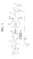
- FIG. 1 is a schematic diagram illustrating a structure of a conventional D-class amplifier circuit.
- the conventional D-class amplifier circuit includes an amplifier 110, a comparator 120, a gate driver 130, a low pass filter (LPF) 140, a triangular wave generator 150, and a limiter 160.
- LPF low pass filter
- the amplifier 110 is realized in the form of an integrator and compares an input signal with an output signal to generate a signal Vea.
- the comparator 120 compares the signal Vea with a triangular wave signal to generate a pulse width modulation (PWM) signal.
- the gate driver 130 amplifies the PWM signal to drive a metal-oxide-semiconductor field-effect transistor (MOSFET) switch.
- MOSFET metal-oxide-semiconductor field-effect transistor
- a signal output from the MOSFET switch, which performs a switching operation according to a gate signal, is low pass filtered by the LPF 140 and applied as an acoustic signal to a speaker SP.
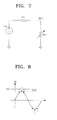
- the limiter 160 may be constituted at an input port to improve a high frequency distortion component generated when an output signal Vo of the conventional D-class amplifier circuit is clipped by a power source.
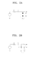
- a general limiter may include general zener diodes ZD1 and ZD2 or general small signal diodes D1 and D2 as shown in Figures 2A and 2B.
- the amplifier 110 having the form of the integrator compares the acoustic signal Vin with a signal fed back from the output signal Vo to generate the signal Vea corresponding to a difference between the acoustic signal Vin and the output signal Vo.
- the amplifier 110 compares the signal Vea with a triangular wave signal to generate a PWM signal, and an output of the amplifier 110 is PWM switched by the PWM signal.
- the PWM signal passes a low pass filter (LPF) 140 so as to reproduce the acoustic signal Vin.
- LPF low pass filter
- the output signal Vo increases with an increase in the acoustic signal Vin. If a peak vertex Vp of the output signal Vo exceeds a power supply voltage VCC due to a further increase in the acoustic signal Vin, the output signal Vo is clipped on an output level corresponding to the power voltage VCC as shown in Figure 3A or 3B. If the conventional D-class amplifier circuit is an analog amplifier circuit not a digital amplifier circuit, the output signal Vo is simply clipped occurs as shown in Figure 3A. Here, the output signal Vo has a distortion component defined as D1.
- the conventional D-class amplifier circuit is a PWM switching amplifier which has been mainly used as a digital amplifier circuit
- the output signal Vo has a waveform as shown in Figure 3B when being clipped and an additional stepped high frequency distortion component D2 at an edge of the clipped portion thereof besides the distortion component D1.
- the generation of the additional stepped high frequency distortion component D2 shown in Figure 3B may be understood with reference to an internal operation waveform of a digital amplifier circuit shown in Figure 4.
- the signal Vea of the amplifier 110 gradually increases and is compared with the triangular wave signal until the output signal Vo is clipped.
- a duty ratio of the PWM signal gradually increases and reaches approximately 100%. Since a point of time when the duty ratio reaches 100% is a point of time when the output signal Vo of the amplifier 110 increases up to the power supply voltage VCC.
- the output signal Vo does not exceeds the power supply voltage VCC and is clipped.
- the signal Vea output from the amplifier 110 exceeds a range of the triangular wave signal and enters a saturation state. If the acoustic signal Vin is attenuated through the peak vertex Vp and a value of the acoustic signal Vin becomes smaller than a feedback value of the clipped output signal Vo, the signal Vea output from the amplifier 110 passes the saturation state and enters the range of the triangular wave signal. A time delay necessarily occurs due to a characteristic of the integrator. The signal Vea is delayed so as to pass the saturation state and enter the range of triangular wave signal.
- the output signal Vo is continuously clipped for the delay time due to the characteristic of the integrator, and the signal Vea output from the amplifier 110 enters the range of the triangular wave signal and then a normal PWM operation. Thereafter, the output signal Vo varies at a steep gradient to rapidly follow an output corresponding to the acoustic signal Vin. Thus, a stepped distortion occurs.
- the signal Vea output from the amplifier 110 must be within the range of the triangular wave to improve the stepped high frequency distortion component D2 generated when the output signal Vea is clipped.
- an input limiter is used to limit the acoustic signal Vin to an appropriate level or less.
- the input limiter may generally have a structure as shown in Figure 2A or 2B. Such a structure is simply constituted, but a level to be limited is limited to a zener voltage or a diode voltage. Thus, it is difficult to freely vary the level. As a result, it is difficult to accurately cope with variations in a gain of an amplifier or a power supply voltage. Also, upper and lower portions of an over-input are clipped during limiting. Thus, an output is distorted.
- An aspect of the present invention prevents or substantially reduces distortion of the output signal by limiting the output level when an over-input occurs.
- an automatic input-gain control circuit for automatically attenuating a gain of an acoustic signal based on a pre-set limited level to minimize a distortion of the acoustic signal caused by clipping of the acoustic signal and limit an over-input of the acoustic signal so as to input the acoustic signal within a dynamic range if the acoustic signal is not input within the dynamic range in an audio apparatus including an acoustic amplifier and a switching amplifier, and a method thereof.
- an automatic input-gain control circuit of an audio amplifier including: an output comparator comparing a voltage of an output signal of the audio amplifier with a reference voltage generated based on a threshold voltage Vth; and an input gain adjuster automatically adjusting a voltage of an input signal of the audio amplifier according to the comparison result of the output comparator so that the voltage of the output signal is within the reference voltage.
- the reference voltage may be a voltage corresponding to a difference between a power supply voltage VCC and the threshold voltage Vth.
- the output comparator may include: a detector detecting whether the voltage of the output signal exceeds the reference voltage; and a transmitter transmitting the voltage of the output signal to the input gain adjuster according to the detection result of the detector.
- the detector may be a constant voltage element, and the constant voltage element may include a zener diode.
- the transmitter may be a switching element, and the switching element may include a transistor.
- the input gain adjuster may be a variable resistor element adjusting an input impedance to attenuate an input gain so that the voltage of the output signal is within the reference voltage if the voltage of the output signal exceeds the reference voltage.
- the variable resistor element may include a junction field effect transistor (J-FET).
- the output comparator may transmit the output signal to the input gain adjuster through the transmitter.
- the output comparator may include: a first comparator comparing the voltage of the output signal with a plus reference voltage; and a second comparator comparing the voltage of the output signal with a minus reference voltage.
- a method of automatically controlling an input gain of an audio amplifier including: comparing a voltage of an output signal of an audio amplifier with a reference voltage generated based on a threshold voltage Vth; and automatically adjusting a voltage of an input signal of the audio amplifier according to the comparison result so that the voltage of the output signal is within the reference voltage.
- the reference voltage may be a voltage corresponding to a difference between a power supply voltage VCC and the threshold voltage Vth.
- the comparing of the voltage of the output signal of the audio amplifier with the reference voltage generated based on the threshold voltage Vth may include: detecting whether the voltage of the output signal exceeds the reference voltage; and outputting the output signal according to the detection result.
- the detecting of whether the voltage of the output signal exceeds the reference voltage may be performed using a constant voltage element.
- the output signal of the audio amplifier may be output using a switching element.
- an input impedance may be adjusted using a variable resistor element to attenuate an input gain so that the voltage of the output signal is within the reference voltage.
- Certain embodiments of the present invention are characterized in that an over-input signal is attenuated to prevent a clipping distortion D1 caused by an over-input and an over-output and a stepped high frequency distortion D2 caused by a saturation of an internal block of the audio amplifier, so that an output signal does not approach a power supply voltage VCC of the audio amplifier but is within a threshold voltage Vth regardless of variations in a gain of the audio amplifier and the power supply voltage VCC. Also, a whole gain may be attenuated instead of cutting over-input components to maintain an original form of the input signal and minimize a distortion of the input signal so as to limit an input level.
- the threshold voltage Vth may be adjusted with respect to the power voltage VCC to vary an output limited level so as to design an amplifier having various output powers depending on products.
- the amplifier may be designed to have the same speaker impedance and power supply voltage as a previously designed amplifier so as to share a speaker and a power source block.
- Figure 5 is a circuit diagram illustrating an automatic input-gain control circuit of an audio amplifier according to an embodiment of the present invention.
- the automatic input-gain control circuit of the audio amplifier according to the present embodiment includes an output comparator 510, an input gain adjuster 520, a switching amplifier 530, and a speaker SP.
- the automatic input-gain control circuit may further include the comparator 120, the gate driver 130, the low pass filter (LPF) 140, and the triangular wave generator 150 as shown in Figure 1. That is, the automatic input-gain control circuit of the present invention may be incorporated in to a prior art device such as the one shown in Figure 1.
- the structures of the comparator 120, the gate driver 130, the LPF 140, and the triangular wave generator 150 have been described above and thus, their detailed descriptions will be omitted herein.
- the output comparator 510 compares a voltage of an output signal Vo (hereinafter called "output voltage") with a reference voltage for inputting an acoustic signal of the audio amplifier within a power supply voltage VCC.
- the output comparator 510 includes first and second comparators 512 and 514 as shown in Figure 5.
- the first comparator 512 compares the output voltage with a threshold voltage Vth of a plus power supply voltage +VCC.
- the second comparator 514 compares the output voltage with a threshold voltage Vth of a minus power supply voltage - VCC.
- the threshold voltages Vth mean margin voltages for disallowing an output signal to reach the power supply voltage VCC.
- the input gain adjuster 520 automatically adjusts a voltage of the acoustic signal to input the acoustic signal within the power supply voltage VCC according to the comparison result of the output comparator 510.
- the input gain adjuster 520 attenuates a whole gain of the acoustic signal so as to maintain an original form of the acoustic signal and minimum a distortion of the acoustic signal.
- the input gain adjuster 520 operates as a voltage control variable resistor Rds for adjusting an input impedance of the acoustic signal.
- the switching amplifier 530 amplifies the acoustic signal.
- the acoustic signal generated by an operation power source is applied to the switching amplifier 530 through an input resistor Rin.
- the output comparator 510 and the speaker SP are connected to an output port of the switching amplifier 530, and the input gain adjuster 520 for adjusting the acoustic signal is connected to an input port of the switching amplifier 530.
- the first comparator 512 of the output comparator 510 is connected to the plus power supply voltage +VCC above the switching amplifier 530, and the second comparator 514 of the output comparator 510 is connected to the minus power supply voltage -VCC under the switching amplifier 530.
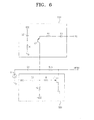
- FIG. 6 is a circuit diagram illustrating an automatic input-gain control circuit according to another embodiment of the present invention.
- the automatic input-gain control circuit according to the present embodiment includes a detection transmitter 610 and an input adjuster 620.
- the detection transmitter 610 and the input adjuster 620 are exemplary implementations of the output comparator 510, and the input gain adjuster 520 of Figure 5 respectively.
- the detection transmitter 610 includes a detector and a transmitter.
- the detector operates when an output voltage exceeds a reference voltage.
- the transmitter is turned on depending on the operation of the detector to transmit the output voltage to the input adjuster 620.
- the reference voltage is a voltage obtained through a subtraction of a threshold voltage Vth from a power supply voltage VCC.
- the reference voltage corresponds to a difference between the power supply voltage VCC and the threshold voltage Vth.
- the detector may be a constant voltage element including a zener diode DZ1
- the transmitter may be a switching element including a transistor Q1.
- the zener diode DZ1 is connected to a resistor R in series between the power supply voltage VCC and a ground voltage, and a base of the transistor Q1 is connected to a connection point between the zener diode DZ1 and the resistor R.
- a diode D1 is connected to a resistor R1 in series between an emitter of the transistor Q1 and an output port, and a collector is connected to the input adjuster 620.
- the transistor Q1 may be a PNP type transistor.
- a capacitor C1 is connected to an input resistor Rin in series between a voltage of an input signal Vin (hereinafter called "input voltage") and an input port INPUT.
- the input adjuster 620 including a junction field effect transistor (J-FET) J1 is connected to a connection point between the input port INPUT and the input resistor Rin.
- the input adjuster 620 may include an element operating as a variable resistor or may include the J-FET J1 as shown in Figure 6.
- a drain of the J-FET J1 of the input adjuster 620 is connected to the connection point between the input port INPUT and the input resistor Rin.
- a source of the J-FET J1 is grounded, and a capacitor C2 is connected to a resistor R in series between a gate and a ground.
- a minus power supply voltage -VCC is connected to a connection point between the capacitor C2 and the resistor R through a resistor R2, and a collector of the transistor Q1 of the detection transmitter 610 is connected to the connection point between the capacitor C2 and the resistor R.
- the equivalent circuit includes an input voltage, an input resistor Rin, and a variable resistor Rds and adjusts an intensity of the input voltage through the variable resistor Rds.
- the automatic input-gain control circuit shown in Figure 6 is constituted as an input part of the audio amplifier shown in Figure 1.
- the automatic input-control circuit operates when the output voltage exceeds the threshold voltage Vth defined as a margin with the power supply voltage VCC.
- the transistor Q1 operates so as to increase a gate voltage of the J-FET J1 of the input adjuster 620.
- V INPUT R ds R in + R ds * V in
- variable resistance Rds decreases with an increase in an over-input state.
- the voltage V INPUT is attenuated.
- a peak value of a substantially output voltage is fixed to and does not exceed the power supply voltage VCC and the threshold voltage Vth.
- a gain of the input signal is attenuated as in Equation 3 to satisfy the conditions of Equation 3.
- Rds is greater than the input resistor Rin, and the voltage V INPUT is equal to the input voltage.
- the input signal is attenuated to be equal to an original acoustic signal and then input to the input port of the audio amplifier.
- an audio apparatus including an acoustic amplifier and a switching amplifier according to the present invention
- a gain of the input acoustic signal is automatically attenuated based on a pre-set limit level so as to input the input acoustic signal within the dynamic range.
- an acoustic signal equal to an original signal is output, a distortion of the acoustic signal is minimized when the acoustic signal is clipped, a stepped distortion is removed, and an over-input is limited.
- an automatic input-gain control circuit and a method thereof according to the present invention only a gain of an over-input signal more than or equal to a specific level can be attenuated instead of cutting the over-input signal.
- a distortion of an output waveform caused by clipping of the output waveform can be minimized.
- a switching amplifier can prevent a saturation of an internal block to simultaneously remove a harmonic distortion and a stepped high frequency noise occurring during clipping.
- a linear analog amplifier can attenuate only the gain with maintaining an original form of the over-input signal instead of simply clipping the over-input signal so as to minimize a distortion of an output signal.
- Electronic appliance having an audio function can use an identical power supply voltage to arbitrarily adjust a reference voltage of an output comparator circuit operating as a gain attenuating circuit so as to limit an output level.
- a power supply voltage and a speaker impedance of a product having various output specifications can be standardized.
Landscapes
- Engineering & Computer Science (AREA)
- Power Engineering (AREA)
- Multimedia (AREA)
- Amplifiers (AREA)
- Tone Control, Compression And Expansion, Limiting Amplitude (AREA)
- Control Of Amplification And Gain Control (AREA)
Applications Claiming Priority (1)
| Application Number | Priority Date | Filing Date | Title |
|---|---|---|---|
| KR1020060046281A KR20070113434A (ko) | 2006-05-23 | 2006-05-23 | 입력이득 자동 제어회로 및 그 방법 |
Publications (2)
| Publication Number | Publication Date |
|---|---|
| EP1860772A2 true EP1860772A2 (fr) | 2007-11-28 |
| EP1860772A3 EP1860772A3 (fr) | 2009-06-03 |
Family
ID=38283643
Family Applications (1)
| Application Number | Title | Priority Date | Filing Date |
|---|---|---|---|
| EP06124011A Withdrawn EP1860772A3 (fr) | 2006-05-23 | 2006-11-14 | Commande de gain d'entrée automatique et méthode |
Country Status (4)
| Country | Link |
|---|---|
| US (1) | US20070273446A1 (fr) |
| EP (1) | EP1860772A3 (fr) |
| KR (1) | KR20070113434A (fr) |
| CN (1) | CN101079602A (fr) |
Cited By (3)
| Publication number | Priority date | Publication date | Assignee | Title |
|---|---|---|---|---|
| CN107666295A (zh) * | 2016-07-27 | 2018-02-06 | 恩智浦有限公司 | 增益校准控制器 |
| EP3721554A4 (fr) * | 2017-12-04 | 2020-12-09 | Aselsan Elektronik Sanayi ve Ticaret Anonim Sirketi | Système de limitation actif |
| CN117241174A (zh) * | 2023-11-10 | 2023-12-15 | 杭州海康威视数字技术股份有限公司 | 音频处理电路和设备 |
Families Citing this family (30)
| Publication number | Priority date | Publication date | Assignee | Title |
|---|---|---|---|---|
| JP5157959B2 (ja) * | 2009-02-27 | 2013-03-06 | ヤマハ株式会社 | D級増幅器 |
| US8570168B2 (en) * | 2009-10-08 | 2013-10-29 | Bringrr Systems, Llc | System, method and device to interrogate for the presence of objects |
| US10244097B2 (en) | 2009-10-08 | 2019-03-26 | Pairable, Inc. | Method and device to set household parameters based on the movement of items |
| CN101969300A (zh) * | 2010-08-25 | 2011-02-09 | 康佳集团股份有限公司 | D类功率放大器的增益调整方法 |
| KR101123343B1 (ko) * | 2010-12-07 | 2012-03-23 | (주)펄서스 테크놀러지 | 고조파를 이용한 디지털 오디오 증폭 장치 및 그 방법 |
| CN103166587A (zh) * | 2011-12-16 | 2013-06-19 | 富泰华工业(深圳)有限公司 | 音频处理电路 |
| WO2013162552A1 (fr) | 2012-04-25 | 2013-10-31 | Hewlett-Packard Development Company, L.P. | Amplificateur à transimpédance et à gain en boucle ouverte, avec impédance d'entrée programmable |
| CN102946578B (zh) * | 2012-11-26 | 2016-03-02 | 成都锐成芯微科技有限责任公司 | 一种免开关pop声的音频耳机放大器 |
| CN103916729A (zh) * | 2012-12-31 | 2014-07-09 | 广州励丰文化科技股份有限公司 | 具有多数字信号处理器的有源音箱 |
| CN103916780A (zh) * | 2012-12-31 | 2014-07-09 | 广州励丰文化科技股份有限公司 | 具有自动降噪功能的高保真有源一体化音箱 |
| CN103916727A (zh) * | 2012-12-31 | 2014-07-09 | 广州励丰文化科技股份有限公司 | 具有多数字信号处理器的有源一体化音箱 |
| CN103973231B (zh) * | 2013-01-31 | 2017-04-26 | 立锜科技股份有限公司 | 放大电路的电压调整电路及相关的调整方法 |
| US9837962B2 (en) * | 2013-06-06 | 2017-12-05 | Qualcomm Incorporated | Envelope tracker with variable boosted supply voltage |
| US10021485B2 (en) * | 2015-11-17 | 2018-07-10 | Cirrus Logic, Inc. | Prevention of signal clipping due to decrease in amplifier supply voltage |
| US9614486B1 (en) * | 2015-12-30 | 2017-04-04 | Amazon Technologies, Inc. | Adaptive gain control |
| WO2018120072A1 (fr) * | 2016-12-30 | 2018-07-05 | Texas Instruments Incorporated | Détecteur d'écrêtage commandé par taux de distorsion harmonique et limiteur automatique de gain (agl) |
| CN108154887B (zh) * | 2017-12-26 | 2021-03-12 | 上海展扬通信技术有限公司 | 一种信息处理方法、装置及终端 |
| TWI686090B (zh) * | 2018-09-26 | 2020-02-21 | 新唐科技股份有限公司 | 偏壓電路 |
| US10972123B1 (en) | 2019-05-09 | 2021-04-06 | Dialog Semiconductor B.V. | Signal processing structure |
| US10861433B1 (en) | 2019-05-09 | 2020-12-08 | Dialog Semiconductor B.V. | Quantizer |
| US10848174B1 (en) | 2019-05-09 | 2020-11-24 | Dialog Semiconductor B.V. | Digital filter |
| US11107453B2 (en) | 2019-05-09 | 2021-08-31 | Dialog Semiconductor B.V. | Anti-noise signal generator |
| US11329634B1 (en) | 2019-05-09 | 2022-05-10 | Dialog Semiconductor B.V. | Digital filter structure |
| US10784890B1 (en) * | 2019-05-09 | 2020-09-22 | Dialog Semiconductor B.V. | Signal processor |
| CN113050184B (zh) * | 2019-12-27 | 2022-06-03 | 欧姆龙(上海)有限公司 | 光电传感器及其控制方法 |
| CN111327937B (zh) * | 2020-04-08 | 2023-08-01 | 山西工程技术学院 | 基于前馈控制的智能型小型音频信号压缩器及实现方法 |
| CN113726339B (zh) * | 2021-08-19 | 2022-06-03 | 江苏润石科技有限公司 | 一种基于误差反馈的失调电压降低方法与数据转换器 |
| US11706062B1 (en) | 2021-11-24 | 2023-07-18 | Dialog Semiconductor B.V. | Digital filter |
| US12057099B1 (en) | 2022-03-15 | 2024-08-06 | Renesas Design Netherlands B.V. | Active noise cancellation system |
| US12483216B2 (en) | 2022-07-27 | 2025-11-25 | Crystal Instruments Corporation | Data recording based on dual ADC architecture |
Family Cites Families (10)
| Publication number | Priority date | Publication date | Assignee | Title |
|---|---|---|---|---|
| JPS6047771B2 (ja) * | 1977-09-20 | 1985-10-23 | ソニー株式会社 | 増幅器の過負荷保護装置 |
| US4301445A (en) * | 1979-12-10 | 1981-11-17 | General Electric Company | Communication system and method having wide dynamic range digital gain control |
| US4459557A (en) * | 1982-02-04 | 1984-07-10 | Mcquilken Mark A | Compressor limiter for audio signal processing |
| US4457203A (en) * | 1982-03-09 | 1984-07-03 | Wright-Malta Corporation | Sound signal automatic detection and display method and system |
| US4509101A (en) * | 1982-08-24 | 1985-04-02 | Nippon Gakki Seizo Kabushiki Kaisha | Protection circuit for switching power amplifier |
| JPS5967719A (ja) * | 1982-10-09 | 1984-04-17 | Nippon Gakki Seizo Kk | パルス幅変調回路 |
| US4881047A (en) * | 1988-06-20 | 1989-11-14 | Waller Jr James K | Automatic gain expansion system |
| US5151939A (en) * | 1990-03-21 | 1992-09-29 | Delco Electronics Corporation | Adaptive audio processor for am stereo signals |
| US5329243A (en) * | 1992-09-17 | 1994-07-12 | Motorola, Inc. | Noise adaptive automatic gain control circuit |
| US6229389B1 (en) * | 1998-11-18 | 2001-05-08 | Intersil Corporation | Class D modulator with peak current limit and load impedance sensing circuits |
-
2006
- 2006-05-23 KR KR1020060046281A patent/KR20070113434A/ko not_active Withdrawn
- 2006-11-14 EP EP06124011A patent/EP1860772A3/fr not_active Withdrawn
- 2006-12-07 CN CNA2006101645663A patent/CN101079602A/zh active Pending
-
2007
- 2007-03-15 US US11/723,016 patent/US20070273446A1/en not_active Abandoned
Cited By (5)
| Publication number | Priority date | Publication date | Assignee | Title |
|---|---|---|---|---|
| CN107666295A (zh) * | 2016-07-27 | 2018-02-06 | 恩智浦有限公司 | 增益校准控制器 |
| CN107666295B (zh) * | 2016-07-27 | 2023-10-24 | 恩智浦有限公司 | 增益校准控制器 |
| EP3721554A4 (fr) * | 2017-12-04 | 2020-12-09 | Aselsan Elektronik Sanayi ve Ticaret Anonim Sirketi | Système de limitation actif |
| CN117241174A (zh) * | 2023-11-10 | 2023-12-15 | 杭州海康威视数字技术股份有限公司 | 音频处理电路和设备 |
| CN117241174B (zh) * | 2023-11-10 | 2024-02-23 | 杭州海康威视数字技术股份有限公司 | 音频处理电路和设备 |
Also Published As
| Publication number | Publication date |
|---|---|
| EP1860772A3 (fr) | 2009-06-03 |
| US20070273446A1 (en) | 2007-11-29 |
| KR20070113434A (ko) | 2007-11-29 |
| CN101079602A (zh) | 2007-11-28 |
Similar Documents
| Publication | Publication Date | Title |
|---|---|---|
| EP1860772A2 (fr) | Commande de gain d'entrée automatique et méthode | |
| EP1865598A2 (fr) | Appareil et procédé de commande de gain d'entrée | |
| US11962275B2 (en) | Amplification systems and methods with distortion reductions | |
| US7142050B2 (en) | Recovery from clipping events in a class D amplifier | |
| US8686792B2 (en) | Amplifying device | |
| EP2587665B1 (fr) | Appareil amplificateur | |
| US8289075B2 (en) | Class-D amplifier | |
| US6838862B2 (en) | Pulse width modulator having reduced signal distortion at low duty cycles | |
| US6107875A (en) | Variable frequency class D modulator with built in soft clipping and frequency limiting | |
| US20030030486A1 (en) | Pulse-width modulation circuit and power amplifier circuit | |
| US20140285258A1 (en) | Silent start class-d amplifier | |
| JP2009049671A (ja) | 出力制限回路、d級パワーアンプ、音響機器 | |
| EP2127070A2 (fr) | Système de traitement de données pour correction d'écrêtage | |
| US7088177B2 (en) | Amplifier apparatus | |
| KR100424359B1 (ko) | D급 증폭기 | |
| US11082019B2 (en) | Amplifier with adaptively-controlled local feedback loop | |
| US7394315B2 (en) | Gate driver for Class D audio amplifier with adaptive dV/dt control | |
| US20110181362A1 (en) | Signal processing circuit | |
| JP4967257B2 (ja) | デジタルアンプ方法及びデジタルアンプ回路 | |
| JP3811030B2 (ja) | デジタルアンプ | |
| KR20110071347A (ko) | 오디오 앰프 출력 제어 장치 및 방법 | |
| EP1973226B1 (fr) | Amplificateur d'alimentation audio et procédé de traitement de signal | |
| US20240213935A1 (en) | Dynamic pulse width control scheme in amplifiers | |
| Jiang et al. | Circuit techniques to overcome class-D audio amplifier limitations in mobile devices | |
| JP2005142795A (ja) | オーディオ回路 |
Legal Events
| Date | Code | Title | Description |
|---|---|---|---|
| PUAI | Public reference made under article 153(3) epc to a published international application that has entered the european phase |
Free format text: ORIGINAL CODE: 0009012 |
|
| AK | Designated contracting states |
Kind code of ref document: A2 Designated state(s): AT BE BG CH CY CZ DE DK EE ES FI FR GB GR HU IE IS IT LI LT LU LV MC NL PL PT RO SE SI SK TR |
|
| AX | Request for extension of the european patent |
Extension state: AL BA HR MK YU |
|
| PUAL | Search report despatched |
Free format text: ORIGINAL CODE: 0009013 |
|
| AK | Designated contracting states |
Kind code of ref document: A3 Designated state(s): AT BE BG CH CY CZ DE DK EE ES FI FR GB GR HU IE IS IT LI LT LU LV MC NL PL PT RO SE SI SK TR |
|
| AX | Request for extension of the european patent |
Extension state: AL BA HR MK RS |
|
| RIC1 | Information provided on ipc code assigned before grant |
Ipc: H03G 11/00 20060101ALI20090424BHEP Ipc: H03F 3/217 20060101ALI20090424BHEP Ipc: H03G 7/00 20060101AFI20070731BHEP |
|
| AKX | Designation fees paid | ||
| REG | Reference to a national code |
Ref country code: DE Ref legal event code: 8566 |
|
| STAA | Information on the status of an ep patent application or granted ep patent |
Free format text: STATUS: THE APPLICATION IS DEEMED TO BE WITHDRAWN |
|
| 18D | Application deemed to be withdrawn |
Effective date: 20091204 |