EP1860920B1 - Dispositif d'éclairage comprenant une source lumineuse et un dispositif tactile et procédé pour opérer un tel dispositif d'éclairage - Google Patents
Dispositif d'éclairage comprenant une source lumineuse et un dispositif tactile et procédé pour opérer un tel dispositif d'éclairage Download PDFInfo
- Publication number
- EP1860920B1 EP1860920B1 EP06010545A EP06010545A EP1860920B1 EP 1860920 B1 EP1860920 B1 EP 1860920B1 EP 06010545 A EP06010545 A EP 06010545A EP 06010545 A EP06010545 A EP 06010545A EP 1860920 B1 EP1860920 B1 EP 1860920B1
- Authority
- EP
- European Patent Office
- Prior art keywords
- time constant
- output
- input
- flip
- flop
- Prior art date
- Legal status (The legal status is an assumption and is not a legal conclusion. Google has not performed a legal analysis and makes no representation as to the accuracy of the status listed.)
- Not-in-force
Links
Images


Classifications
-
- H—ELECTRICITY
- H05—ELECTRIC TECHNIQUES NOT OTHERWISE PROVIDED FOR
- H05B—ELECTRIC HEATING; ELECTRIC LIGHT SOURCES NOT OTHERWISE PROVIDED FOR; CIRCUIT ARRANGEMENTS FOR ELECTRIC LIGHT SOURCES, IN GENERAL
- H05B45/00—Circuit arrangements for operating light-emitting diodes [LED]
- H05B45/30—Driver circuits
- H05B45/32—Pulse-control circuits
Definitions
- the present invention relates to a lighting device with a light source and a touch device, which comprises a button, a connection for a supply voltage and a D flip-flop, wherein the D flip-flop a set input, a reset input, a clock Input, a data input, a Q output and a Qbar output, with the light source connected to the Q output or the Qbar output. It also relates to a method for operating such a lighting device.
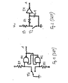
- Fig. 1 shows a sensing device comprising a button T1, in particular a changeover switch, and two pull-up resistors R1, R2 and two cross-coupled NAND gates, which together form an R / S flip-flop.
- the light source not shown, is to be coupled to the output A, for example directly or via a switching transistor or an electronic switching element.
- the sensing device shown is that the button T1 must be multi-pole, ie as a switch, trained, which is too expensive for a variety of applications.
- a pushbutton T2 and an inverter I1 are used.
- the bounce time of the button T2 must be known.
- the RC element must be matched to the T2 button and the switching thresholds of the I1 inverter, so that debouncing works reliably. If, in fact, the RC element is too short, ie dimensioned with too short a time constant, the feeler device switches again when bouncing. A too slow dimensioning results in an undesirable dead time.
- the design for fast switching operations which is characterized by the use of a small-sized capacitor C, is sensitive to RF couplings on the switch leads and due to a shift of the trigger threshold voltage dips of the supply voltage U v , for example, load changes.
- the present invention is therefore based on the object, the lighting device mentioned above in such a way that it avoids the disadvantages of the prior art and in particular by a cost-effective implementation and characterized in that a reliable debouncing can be ensured regardless of the bounce time.
- Another object of the invention is to provide a corresponding method for operating a lighting device mentioned above.
- the invention is based on the finding that these objects can be achieved if a first timer with a first time constant and a second timer with a second time constant are used, wherein the second time constant is greater than the first time constant.
- the first timer is connected on the one hand via the button to the connection for the supply voltage and on the other hand to the clock input.
- the second timer is coupled between the Qbar output and the data input. If the D flip-flop is in the reset state, pressing the button over the first timer generates a pulse-shaped voltage signal, which is applied to the clock input of the D flip-flop. The first rising edge of this signal triggers the D flip-flop, i. H.
- the level at the data input is polled synchronously with the pulse at the clock input and the Q output is switched to the level at the data input. Since in the reset state of the D flip-flop the Q output is low and the Qbar output is high, the high signal of the Qbar output is connected via the second timer to the data input of the D flip-flop created. In this "reset" state of the D flip-flop, the first pulse on the clock input triggers a switching operation of the D flip-flop, in which the signals at the Q output and Qbar output change. The Q output goes high, the Qbar output low. The data input initially remains at the previous level (High) due to the second time constant.
- the measure according to the invention effectively suppresses all pulse edges caused by trigger bounces, RF disturbances, voltage dips or load changes at the clock input.
- the debouncing is also independent of the impedance of the probe. It is insensitive to the amount of supply voltage, which is of particular importance for battery-powered systems but also for supply from power sources with higher output impedance, such as small power adapters.
- the implementation according to the invention is independent of the switching thresholds of the D flip-flops used. Because the first edge from low to high at the clock input triggers the D-flip-flop. Subsequent triggers are no longer accepted during the time period of the second time constant. From the first trigger on the clock input, this means a shift in the threshold due to the load change for subsequent pulses without any effect on the switching state of the D flip-flop.
- a particularly preferred embodiment is characterized in that the second time constant is at least 10 times, in particular at least 50 times, the first time constant. This variant ensures for a particularly long time that the data input remains at the high level until all the bounce pulses generated by pressing the button at the clock input of the D flip-flop have decayed safely.
- a third timer with a third time constant is provided, which is coupled between the connection for the supply voltage and the reset input. It is particularly preferred if the third time constant is at least 10 times, in particular at least 50 times, the first time constant. This ensures that a new reset pulse can be generated immediately after a shutdown or interruption of the supply voltage when restarting.
- At least one timer is implemented as an RC element and / or an LR element.
- RC elements or LR links are inexpensive to implement and easy to dimension.
- At least one timer comprises a first and a second ohmic resistor in series, wherein the first ohmic resistor, a capacitor is connected in parallel and the connection point between the first and the second ohmic resistor, the output and the point of departure facing away from this connection point between the first ohmic resistance and the capacitor represents the input of the respective timer.
- the set input is coupled to a reference potential, in particular to the ground potential.
- Fig. 3 shows an embodiment of a lighting device according to the invention in a schematic representation. It comprises a pushbutton T3, which is connected between the supply voltage connection U v and a first timer, which comprises the resistors R5, R6 and the capacitor C2 and with which a first time constant ⁇ 1 is realized.
- the resistor R5 and the capacitor C2 are connected in parallel, wherein the voltage drop across the resistor R6 is supplied to the clock input of a D flip-flop 10.
- the D flip-flop also has a reset input, a data input, a set input, a Q output and a Qbar output.
- the Qbar output is connected to the data input via a second timer comprising resistor R7 and capacitor C3, which together form a second time constant ⁇ 2.
- the set input is at a reference potential, in this case ground.
- the Q output represents a terminal A for connecting the light source La.
- the output A is coupled to the gate of a transistor T4 via a voltage divider comprising the resistors R10 and R11.
- the source terminal of the transistor T4 is connected to the ground terminal, while between the drain terminal and the supply voltage U v, the light source La is arranged, which in the present case comprises four series-connected LEDs.
- the light source could also be coupled directly to the output A.
- the reset input is connected to the supply voltage terminal U v via a third timer, which comprises the resistors R8 and R9 and the capacitor C4 and forms a third time constant ⁇ 3.
- the D-type flip-flop 10 is reset at startup of the lighting device. For this purpose, a single reset pulse is generated with the aid of the components R8, C4 and R9 when the supply voltage is switched on.
- the charging current generated at the resistor R9 a voltage drop, which is present as a signal at the reset input of the D flip-flop 10 and resets it.
- At the Q output of the reset D flip-flop 10 is a low signal, at the Qbar output corresponding to a high signal.
- a low voltage corresponding to the voltage divider from the resistors R8 and R9 sets at the reset input, for example, 0.1 * U v .
- the clock input of the D flip-flop 10 is enabled.
- a switching operation of the D-type flip-flop 10 can now take place when the pushbutton T3 is pressed.
- the data input initially remains at the previous level (high), since the capacitor C3 must first discharge via the resistor R7 with the time constant ⁇ 2. During this period of time, voltage pulses arriving at the clock input can not switch again since the data input is still at the high level. Due to the delayed due to the time constant ⁇ 2 level change at the data input all caused by Tasterprellen, RF interference, voltage dips or load changes pulse edges are effectively suppressed at the clock input.
- Debouncing is also insensitive to the level of the supply voltage.
- the switching threshold of the clock input of the D flip-flop must be exceeded by a pulse triggered by a switching operation of the button, at least once so that the flip-flop then - at the first such pulse - switches.
- the dimensioning of R5, C2, R6 ensures that this pulse triggered by the probe always has a sufficiently high amplitude to trigger a switching operation of the D flip-flop, even if the supply voltage U v is in a wide range, for example between 8 V and 18 V DC, varies.
- ⁇ 1 is 0.1 ms
- ⁇ 2 is 10 ms
- ⁇ 3 is 10 ms
- ⁇ 4 100 ms
- R10 is 100 ⁇
- R11 is 1 M ⁇ .
- FIGS. 4 to 7 show the time courses of the signals at the clock input U Cl , at the data input U D and at the Q output U Q for an embodiment of a lighting device according to the invention, wherein the temporal resolution in the FIGS. 4 and 5 20.0 ms, in the FIGS. 6 and 7 10.0 ⁇ s.
- Fig. 4 shows the time course of said three signals at a power-up after a reset. Over time, the voltage U Cl of the pulse generated by pressing the button T3 can be seen initially at time t1. This leads to a switching of the D flip-flops, as can be seen on the time course of the voltage U Q.
- the not shown voltage at the Qbar output changes in the opposite way, ie while U Q goes from low to high, U Qbar goes from high to low.
- the change in the voltage U Qbar at the output Qbar is only delayed given to the data input as a result of the time determined by the capacitor C3 and the resistor R7 time constant ⁇ 2, as well to be recognized by the time course of the voltage U D.
- Fig. 5 shows the timing of the above signals at a turn-off of the D-type flip-flop 10.
- the D flip-flop 10 switches; the voltage U Q at the Q output goes from high to low.
- the voltage at the Qbar output changes in the opposite way, ie it goes from low to high. This change is in turn passed through the capacitor C3 and the resistor R7 fixed time constant ⁇ 2 only delayed to the data input, as well to recognize by the time course of the voltage U D.
- FIGS. 6 and 7 the time course of said signals in much greater resolution, each at a power-up.
- the resolution is so great that the reduction in the amplitude of the voltage U D is barely discernible (which, however, in view of the Presentation in the FIGS. 6 and 7 is not relevant).
- Fig. 6 clearly shows that a button bouncing, ie several consecutive pulses at the clock input, see the course of the voltage U Cl , reliably do not lead to a corresponding switching of the D flip-flop. This can be seen from the fact that the voltage U Q at the Q output does not change again after a first change, despite the sequence of pulses at the clock input. The reason is that at the time of the repeated pulses at the clock input, the data input is still high, see the corresponding amplitude of the voltage U D.
- Fig. 7 shows another example:
- a clearly pronounced second rising edge at time t2 occurs.
- this second rising edge does not lead to a renewed switching of the D flip-flop 10.
- the cause is in turn that at time t2 of the occurrence of the second rising edge, the voltage U D is still high at the signal input of the D flip-flop.
Landscapes
- Electronic Switches (AREA)
- Push-Button Switches (AREA)
- Circuit Arrangement For Electric Light Sources In General (AREA)
Claims (9)
- Dispositif d'éclairage ayant une source lumineuse et un dispositif à touche qui comprend une touche, une borne pour une tension d'alimentation et une bascule D ( 10 ), la bascule D ( 10 ) ayant une entrée de mise à un, une entrée de remise à zéro, une entrée d'horloge, une entrée de données, une sortie Q et une sortie Qbar, la source lumineuse étant raccordée à la sortie Q ou à la sortie Qbar,
caractérisé
en ce qu'il comprend en outre :- un premier élément ( C2, R6 ) temporisateur, ayant une première constante de temps ( τ1 ) qui peut être relié d'une part, par la touche ( T3 ), à la borne ( Uv ) pour la tension d'alimentation et, d'autre part, à l'entrée d'horloge ;- un deuxième élément ( R7, C3 ) temporisateur ayant une deuxième constante ( τ2 ), qui est monté entre la sortie Qbar et l'entrée de données ;la deuxième constante ( τ2 ) étant plus grande que la première constante de temps ( τ1 ). - Dispositif d'éclairage suivant la revendication 1,
caractérisé
en ce que la deuxième constante de temps ( τ2 ) représente au moins 10 fois, notamment au moins 50 fois, la première constante de temps ( τ1 ). - Dispositif d'éclairage suivant l'une des revendications 1 et 2,
caractérisé
en ce qu'il comprend un troisième élément ( C4, R9 ) temporisateur, ayant une troisième constante de temps ( τ3 ), qui est monté entre la borne pour la tension d'alimentation et l'entrée de remise à zéro. - Dispositif d'éclairage suivant la revendication 3,
caractérisé
en ce que la troisième constante de temps ( τ3 ) représente au moins 10 fois, notamment au moins 50 fois, la première constante de temps ( τ1 ). - Dispositif d'éclairage suivant l'une des revendications 3 ou 4,
caractérisé
en ce que la troisième constante de temps ( τ3 ) est d'au moins 10 ms, de préférence comprise entre 10 ms et 50 ms. - Dispositif d'éclairage suivant l'une des revendications précédentes,
caractérisé
en ce qu'au moins un élément temporisateur est réalisé en élément RC ( C2, R6 ; C4, R9 ; C3, R7 ) et/ou en élément LR. - Dispositif d'éclairage suivant l'une des revendications précédentes,
caractérisé
en ce qu'au moins un élément temporisateur comprend une première ( R5, R8 ) et une deuxième résistance ohmique montées en série ( R5, R6, R8, R9 ), un condensateur ( C2, C4 ) étant monté en parallèle à la première résistance ( R5, R8 ) ohmique et le point de liaison entre la première ( R5, R8 ) et la deuxième résistance ( R6, R9 ) ohmique représentant la sortie et le point de liaison, éloigné de ce point de liaison et compris entre la première résistance ( R5, R8 ) ohmique et le condensateur ( C2, C4 ), représentant l'entrée de l'élément temporisateur respectif. - Dispositif d'éclairage suivant l'une des revendications précédentes,
caractérisé
en ce que l'entrée de mise à un est couplée à un potentiel de référence, notamment au potentiel de masse. - Procédé pour faire fonctionner un dispositif d'éclairage ayant une source lumineuse et un dispositif à touche qui comprend une touche, une borne pour une tension d'alimentation et une bascule D ( 10 ), la bascule D ( 10 ) ayant une entrée de mise à un, une entrée de remise à zéro, une entrée d'horloge, une entrée de données, une sortie Q et une sortie Qbar, la source lumineuse étant raccordée à la sortie Q ou à la sortie Qbar,
caractérisé par les stades suivants :a) on appuie sur la touche pour relier la borne pour la tension d'alimentation à l'entrée d'horloge par l'intermédiaire d'un premier élément ( C2, R6 ) temporisateur ayant une première constante de temps ( τ1 ) ;b) on applique le signal à la sortie Qbar par l'intermédiaire d'un deuxième élément ( R7, C3 ) temporisateur ayant une deuxième constante de temps ( τ2 ) qui est plus grande que la première constante de temps ( τ1 ) à l'entrée de données.
Priority Applications (3)
| Application Number | Priority Date | Filing Date | Title |
|---|---|---|---|
| EP06010545A EP1860920B1 (fr) | 2006-05-22 | 2006-05-22 | Dispositif d'éclairage comprenant une source lumineuse et un dispositif tactile et procédé pour opérer un tel dispositif d'éclairage |
| AT06010545T ATE431063T1 (de) | 2006-05-22 | 2006-05-22 | Beleuchtungsvorrichtung mit einer lichtquelle und einer tastvorrichtung und verfahren zum betreiben einer derartigen beleuchtungsvorrichtung |
| DE502006003664T DE502006003664D1 (de) | 2006-05-22 | 2006-05-22 | Beleuchtungsvorrichtung mit einer Lichtquelle und einer Tastvorrichtung und Verfahren zum Betreiben einer derartigen Beleuchtungsvorrichtung |
Applications Claiming Priority (1)
| Application Number | Priority Date | Filing Date | Title |
|---|---|---|---|
| EP06010545A EP1860920B1 (fr) | 2006-05-22 | 2006-05-22 | Dispositif d'éclairage comprenant une source lumineuse et un dispositif tactile et procédé pour opérer un tel dispositif d'éclairage |
Publications (2)
| Publication Number | Publication Date |
|---|---|
| EP1860920A1 EP1860920A1 (fr) | 2007-11-28 |
| EP1860920B1 true EP1860920B1 (fr) | 2009-05-06 |
Family
ID=37309512
Family Applications (1)
| Application Number | Title | Priority Date | Filing Date |
|---|---|---|---|
| EP06010545A Not-in-force EP1860920B1 (fr) | 2006-05-22 | 2006-05-22 | Dispositif d'éclairage comprenant une source lumineuse et un dispositif tactile et procédé pour opérer un tel dispositif d'éclairage |
Country Status (3)
| Country | Link |
|---|---|
| EP (1) | EP1860920B1 (fr) |
| AT (1) | ATE431063T1 (fr) |
| DE (1) | DE502006003664D1 (fr) |
Family Cites Families (1)
| Publication number | Priority date | Publication date | Assignee | Title |
|---|---|---|---|---|
| DD263401A1 (de) * | 1987-07-29 | 1988-12-28 | Zeiss Jena Veb Carl | Integrationsfaehige schaltungsanordnung zur synchronen entprellung von schaltvorgaengen |
-
2006
- 2006-05-22 EP EP06010545A patent/EP1860920B1/fr not_active Not-in-force
- 2006-05-22 AT AT06010545T patent/ATE431063T1/de active
- 2006-05-22 DE DE502006003664T patent/DE502006003664D1/de active Active
Also Published As
| Publication number | Publication date |
|---|---|
| ATE431063T1 (de) | 2009-05-15 |
| EP1860920A1 (fr) | 2007-11-28 |
| DE502006003664D1 (de) | 2009-06-18 |
Similar Documents
| Publication | Publication Date | Title |
|---|---|---|
| DE102011003733B4 (de) | Verfahren zur Ansteuerung eines Transistors und Ansteuerschaltung | |
| EP0185667B1 (fr) | Remise a l'etat initial d'un microprocesseur | |
| DE3708499C2 (fr) | ||
| DE102010060527B3 (de) | Schaltungsanordnung zum Nachweis einzelner Photonen | |
| DE112014001233T5 (de) | Treiberschaltkreis und Halbleitervorrichtung | |
| DE3924653C2 (fr) | ||
| EP1860920B1 (fr) | Dispositif d'éclairage comprenant une source lumineuse et un dispositif tactile et procédé pour opérer un tel dispositif d'éclairage | |
| DE3839077C2 (fr) | ||
| DE4106690A1 (de) | Verfahren zur steuerung einer last sowie eine schaltungsanordnung zur durchfuehrung dieses verfahrens mit einem igbt-transistor | |
| DE19905053C2 (de) | Komparatorschaltung | |
| DE102004060211A1 (de) | Integrierte Schaltung mit einem Unterspannungsdetektor | |
| DE102010012529B3 (de) | Schaltungsanordnung für einen Optokoppler | |
| EP3639779A1 (fr) | Instrument de coagulation et de dissection de tissu biologique | |
| DE102004010890B4 (de) | Verfahren und Schaltungsanordnung zum Umschalten eines elektrischen Schaltkreises in einen Stromsparmodus | |
| DE10343278B4 (de) | Halbbrückenschaltung mit einer Einrichtung zur Vermeidung von Querströmen | |
| EP0660042B1 (fr) | Circuit de couplage de lignes sous tension avec un micro-processeur | |
| DE3837080C2 (fr) | ||
| EP1921900B1 (fr) | Dispositif d'éclairage doté d'une source lumineuse et d'un interrupteur à effleurement | |
| DE2834953C2 (fr) | ||
| DE19754927C2 (de) | Schaltungsanordnung zur Leerlauferfassung | |
| EP1086477B1 (fr) | Circuit d'entree pour signaux de courant alternatif a intensite relativement elevee a surveiller | |
| DE102005024550A1 (de) | Hardwarekonzept einer Reset-Schaltung | |
| DE2546620C2 (fr) | ||
| DE102009023805B4 (de) | Schaltungsvorrichtung mit der Funktion eines nachtriggerbaren Univibrators | |
| DE2950700C2 (de) | Anordnung zur Beeinflussung des Abschaltverhaltens von Transistorstufen |
Legal Events
| Date | Code | Title | Description |
|---|---|---|---|
| PUAI | Public reference made under article 153(3) epc to a published international application that has entered the european phase |
Free format text: ORIGINAL CODE: 0009012 |
|
| AK | Designated contracting states |
Kind code of ref document: A1 Designated state(s): AT BE BG CH CY CZ DE DK EE ES FI FR GB GR HU IE IS IT LI LT LU LV MC NL PL PT RO SE SI SK TR |
|
| AX | Request for extension of the european patent |
Extension state: AL BA HR MK YU |
|
| 17P | Request for examination filed |
Effective date: 20071214 |
|
| AKX | Designation fees paid |
Designated state(s): AT DE FR GB IT SE |
|
| GRAP | Despatch of communication of intention to grant a patent |
Free format text: ORIGINAL CODE: EPIDOSNIGR1 |
|
| RAP1 | Party data changed (applicant data changed or rights of an application transferred) |
Owner name: OSRAM GESELLSCHAFT MIT BESCHRAENKTER HAFTUNG |
|
| GRAS | Grant fee paid |
Free format text: ORIGINAL CODE: EPIDOSNIGR3 |
|
| GRAA | (expected) grant |
Free format text: ORIGINAL CODE: 0009210 |
|
| AK | Designated contracting states |
Kind code of ref document: B1 Designated state(s): AT DE FR GB IT SE |
|
| REG | Reference to a national code |
Ref country code: GB Ref legal event code: FG4D Free format text: NOT ENGLISH |
|
| REF | Corresponds to: |
Ref document number: 502006003664 Country of ref document: DE Date of ref document: 20090618 Kind code of ref document: P |
|
| REG | Reference to a national code |
Ref country code: SE Ref legal event code: TRGR |
|
| PLBE | No opposition filed within time limit |
Free format text: ORIGINAL CODE: 0009261 |
|
| STAA | Information on the status of an ep patent application or granted ep patent |
Free format text: STATUS: NO OPPOSITION FILED WITHIN TIME LIMIT |
|
| 26N | No opposition filed |
Effective date: 20100209 |
|
| PGFP | Annual fee paid to national office [announced via postgrant information from national office to epo] |
Ref country code: AT Payment date: 20110408 Year of fee payment: 6 |
|
| PGFP | Annual fee paid to national office [announced via postgrant information from national office to epo] |
Ref country code: IT Payment date: 20110526 Year of fee payment: 6 |
|
| REG | Reference to a national code |
Ref country code: DE Ref legal event code: R081 Ref document number: 502006003664 Country of ref document: DE Owner name: OSRAM GMBH, DE Free format text: FORMER OWNER: OSRAM GESELLSCHAFT MIT BESCHRAENKTER HAFTUNG, 81543 MUENCHEN, DE Effective date: 20111213 |
|
| REG | Reference to a national code |
Ref country code: AT Ref legal event code: MM01 Ref document number: 431063 Country of ref document: AT Kind code of ref document: T Effective date: 20120522 |
|
| PG25 | Lapsed in a contracting state [announced via postgrant information from national office to epo] |
Ref country code: AT Free format text: LAPSE BECAUSE OF NON-PAYMENT OF DUE FEES Effective date: 20120522 |
|
| PG25 | Lapsed in a contracting state [announced via postgrant information from national office to epo] |
Ref country code: IT Free format text: LAPSE BECAUSE OF NON-PAYMENT OF DUE FEES Effective date: 20120522 |
|
| REG | Reference to a national code |
Ref country code: DE Ref legal event code: R081 Ref document number: 502006003664 Country of ref document: DE Owner name: OSRAM GMBH, DE Free format text: FORMER OWNER: OSRAM AG, 81543 MUENCHEN, DE Effective date: 20130205 |
|
| REG | Reference to a national code |
Ref country code: DE Ref legal event code: R081 Ref document number: 502006003664 Country of ref document: DE Owner name: OSRAM GMBH, DE Free format text: FORMER OWNER: OSRAM GMBH, 81543 MUENCHEN, DE Effective date: 20130823 |
|
| REG | Reference to a national code |
Ref country code: FR Ref legal event code: PLFP Year of fee payment: 11 |
|
| REG | Reference to a national code |
Ref country code: FR Ref legal event code: PLFP Year of fee payment: 12 |
|
| PGFP | Annual fee paid to national office [announced via postgrant information from national office to epo] |
Ref country code: FR Payment date: 20170523 Year of fee payment: 12 Ref country code: GB Payment date: 20170519 Year of fee payment: 12 Ref country code: DE Payment date: 20170523 Year of fee payment: 12 |
|
| PGFP | Annual fee paid to national office [announced via postgrant information from national office to epo] |
Ref country code: SE Payment date: 20170519 Year of fee payment: 12 |
|
| REG | Reference to a national code |
Ref country code: DE Ref legal event code: R119 Ref document number: 502006003664 Country of ref document: DE |
|
| REG | Reference to a national code |
Ref country code: SE Ref legal event code: EUG |
|
| GBPC | Gb: european patent ceased through non-payment of renewal fee |
Effective date: 20180522 |
|
| PG25 | Lapsed in a contracting state [announced via postgrant information from national office to epo] |
Ref country code: SE Free format text: LAPSE BECAUSE OF NON-PAYMENT OF DUE FEES Effective date: 20180523 |
|
| PG25 | Lapsed in a contracting state [announced via postgrant information from national office to epo] |
Ref country code: GB Free format text: LAPSE BECAUSE OF NON-PAYMENT OF DUE FEES Effective date: 20180522 Ref country code: DE Free format text: LAPSE BECAUSE OF NON-PAYMENT OF DUE FEES Effective date: 20181201 Ref country code: FR Free format text: LAPSE BECAUSE OF NON-PAYMENT OF DUE FEES Effective date: 20180531 |