EP1863171A1 - Amplificateur opérationnel en classe AB - Google Patents
Amplificateur opérationnel en classe AB Download PDFInfo
- Publication number
- EP1863171A1 EP1863171A1 EP06011220A EP06011220A EP1863171A1 EP 1863171 A1 EP1863171 A1 EP 1863171A1 EP 06011220 A EP06011220 A EP 06011220A EP 06011220 A EP06011220 A EP 06011220A EP 1863171 A1 EP1863171 A1 EP 1863171A1
- Authority
- EP
- European Patent Office
- Prior art keywords
- operational amplifier
- voltage reference
- transistors
- transistor
- vdd
- Prior art date
- Legal status (The legal status is an assumption and is not a legal conclusion. Google has not performed a legal analysis and makes no representation as to the accuracy of the status listed.)
- Withdrawn
Links
- 230000003044 adaptive effect Effects 0.000 claims abstract description 24
- 239000003990 capacitor Substances 0.000 claims description 5
- 101150108692 GDS gene Proteins 0.000 description 6
- 230000007246 mechanism Effects 0.000 description 5
- 230000001419 dependent effect Effects 0.000 description 3
- 238000004088 simulation Methods 0.000 description 3
- 101100228853 Saccharolobus solfataricus (strain ATCC 35092 / DSM 1617 / JCM 11322 / P2) gds gene Proteins 0.000 description 2
- 230000008901 benefit Effects 0.000 description 2
- 238000010586 diagram Methods 0.000 description 2
- 238000000034 method Methods 0.000 description 2
- 230000004044 response Effects 0.000 description 2
- 238000000926 separation method Methods 0.000 description 2
- 230000001052 transient effect Effects 0.000 description 2
- 230000008859 change Effects 0.000 description 1
- 230000001010 compromised effect Effects 0.000 description 1
- 230000007423 decrease Effects 0.000 description 1
- 230000000694 effects Effects 0.000 description 1
- 230000003071 parasitic effect Effects 0.000 description 1
- 230000008569 process Effects 0.000 description 1
- 238000004513 sizing Methods 0.000 description 1
Images



Classifications
-
- H—ELECTRICITY
- H03—ELECTRONIC CIRCUITRY
- H03F—AMPLIFIERS
- H03F3/00—Amplifiers with only discharge tubes or only semiconductor devices as amplifying elements
- H03F3/45—Differential amplifiers
- H03F3/45071—Differential amplifiers with semiconductor devices only
- H03F3/45076—Differential amplifiers with semiconductor devices only characterised by the way of implementation of the active amplifying circuit in the differential amplifier
- H03F3/45179—Differential amplifiers with semiconductor devices only characterised by the way of implementation of the active amplifying circuit in the differential amplifier using MOSFET transistors as the active amplifying circuit
- H03F3/45183—Long tailed pairs
-
- H—ELECTRICITY
- H03—ELECTRONIC CIRCUITRY
- H03F—AMPLIFIERS
- H03F2200/00—Indexing scheme relating to amplifiers
- H03F2200/456—A scaled replica of a transistor being present in an amplifier
-
- H—ELECTRICITY
- H03—ELECTRONIC CIRCUITRY
- H03F—AMPLIFIERS
- H03F2200/00—Indexing scheme relating to amplifiers
- H03F2200/513—Indexing scheme relating to amplifiers the amplifier being made for low supply voltages
-
- H—ELECTRICITY
- H03—ELECTRONIC CIRCUITRY
- H03F—AMPLIFIERS
- H03F2203/00—Indexing scheme relating to amplifiers with only discharge tubes or only semiconductor devices as amplifying elements covered by H03F3/00
- H03F2203/45—Indexing scheme relating to differential amplifiers
- H03F2203/45448—Indexing scheme relating to differential amplifiers the common source circuit [CSC] comprising an addition circuit made by mirrors
-
- H—ELECTRICITY
- H03—ELECTRONIC CIRCUITRY
- H03F—AMPLIFIERS
- H03F2203/00—Indexing scheme relating to amplifiers with only discharge tubes or only semiconductor devices as amplifying elements covered by H03F3/00
- H03F2203/45—Indexing scheme relating to differential amplifiers
- H03F2203/45454—Indexing scheme relating to differential amplifiers the CSC comprising biasing means controlled by the input signal
-
- H—ELECTRICITY
- H03—ELECTRONIC CIRCUITRY
- H03F—AMPLIFIERS
- H03F2203/00—Indexing scheme relating to amplifiers with only discharge tubes or only semiconductor devices as amplifying elements covered by H03F3/00
- H03F2203/45—Indexing scheme relating to differential amplifiers
- H03F2203/45644—Indexing scheme relating to differential amplifiers the LC comprising a cross coupling circuit, e.g. comprising two cross-coupled transistors
-
- H—ELECTRICITY
- H03—ELECTRONIC CIRCUITRY
- H03F—AMPLIFIERS
- H03F2203/00—Indexing scheme relating to amplifiers with only discharge tubes or only semiconductor devices as amplifying elements covered by H03F3/00
- H03F2203/45—Indexing scheme relating to differential amplifiers
- H03F2203/45648—Indexing scheme relating to differential amplifiers the LC comprising two current sources, which are not cascode current sources
Definitions
- the present invention relates to an operational amplifier of class AB, in particular for low voltage application.
- the invention relates to an operational amplifier of class AB including a core of the OTA type which comprises:
- the op-amps have to charge large capacitive loads. In these cases, the op-amps have to tracks large signal in a limited time slot.
- He known op-amps can be substantially divided in two main groups or classy, namely the A and AB class of amplifiers.
- Class A op-amps have poor behavior with large signals due to their constant tail current and thus they show a transient response being slew-rate limited, as described by KLINKE et al. in the article entitled: "A Very-High- Slew-Rate CMOS Operational Amplifier", IEEE Journal of Solid- State Circuits, vol. 24, no. 3, June 1989 .
- circuit topology described in this article being a class AB op-amp, easily overcomes slew rate problems.
- a circuit has a maximum output current which is not well controlled: this could be a problem in low-power applications, especially where a portable system with a battery aboard is concerned.
- the technical problem underlying the present invention is that of providing an operational amplifier based on the adaptive bias principle and having structural and functional characteristics which allow to reduce its power consumption and, in a same time, enhance its DC-gain, in this way overcoming the limits which still affect the amplifiers realised according to the prior art.
- the solution idea underlying the present invention is that of providing an operational amplifier having a fully symmetrical core, in particular realised by an OTA in order to reduce its power consumption connected to a adaptive bias block implementing the adaptive bias principle and comprising a positive feedback biasing block in order to enhance the DC-gain of the operational amplifier.
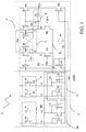
- the op-amp 1 essentially comprises a core 2 and an adaptive bias block 3, inserted between a first and a second voltage reference, in particular a supply voltage reference Vdd and ground GND, and interconnected in correspondence of a first common node X1.
- the core 2 is realised by an OTA (Operational Transconductance Amplifier), as shown in Figure 2, also indicated with 2. More particularly, the core 2 is a CMOS OTA with a symmetrical input stage comprising a first and a second input transistors M 1 and M2.
- OTA Operaational Transconductance Amplifier
- These input transistors M1 and M2 are inserted between respective first and second internal nodes, A and B, and the first common node X1 and have control or gate terminals connected to a first IN- and a second input terminal IN+ of the op-amp 1.
- the OTA 2 also comprises a first and a second input load stage transistors M3 and M4 diode connected and inserted between the supply voltage reference Vdd and respective conductive terminals, in particular drain terminals of the input transistors M1 and M2 in correspondence with the first and second internal nodes, A and B.
- the first input stage load transistor M3 has a control or gate terminal connected to a control or gate terminal of a mirror transistor M5, in turn connected between to the supply voltage reference Vdd and a second common node X2.
- the first input stage load transistor M4 has a control or gate terminal connected to a control or gate terminal of a first output transistor M6, in turn connected between to the supply voltage reference Vdd and aa output terminal OUT of the op-amp 1.
- a biasing transistor M7 is inserted between the second common node X2 and ground GND and has a control or gate terminal connected to the second common node X2 and to a control gate of a second output transistor M8 being in turn inserted between the output terminal OUT and ground GND.
- the OTA 2 has an input stage 4A comprising the input transistors M 1 and M2 and an output stage 4B comprising the first and second transistors M6 and M8, as well as an input stage load 4C comprising the first and second input stage load transistors M3 and M4.
- the first common node X 1 is also connected to ground GND through a generator of a bias current Ib, also indicated as tail current generator G1.
- the current flowing in the transistors M5 and M6 is made K1 times greater than the current flowing in the first and second input stage load transistors M3 and M4, in order to obtain a GBW (Gain BandWidth) K1 times the GBW of a standard OTA configuration. It is however verified that the total power consumption of such an OTA 2 is (K1+1) times larger as well, factor K1 being normally increased to increase the slew rate.
- the first and second internal nodes, A and B, are at low impedance, so a dominant pole of the transconductance function of the op-amp 1 is due to an output impedance of the OTA 2.
- the op-amp 1 exploits the adaptive bias principle, as described above, by using an adaptive bias block 3 connected to first common node X1.
- a current subtractor is used, as shown in Figure 3, globally indicated with 5.
- the current subtractor 5 comprises first and second additional transistors, N1 and N2, having respective control or gate terminals and first conductive terminals, in particular source terminals, in common, the common source terminals being connected to ground GND.
- the first additional transistor N1 has a second conductive terminal, in particular a drain terminal connected to its gate terminal and receiving a current, which is a copy of the current flowing in the first input transistor M1 of the OTA 2 and is also labelled as I1.
- the second additional transistor N2 also has a second conductive terminal, in particular a drain terminal receiving a current, which is a copy of the current flowing in the second input transistor M2 of the OTA 2 and is also labelled as 12.
- the current subtractor 5 further comprises third and fourth additional transistors, N3 and N4, having respective control or gate terminals and first conductive terminals, in particular source terminals, in common, the common source terminals being connected to ground GND.
- the third additional transistor N3 has a second conductive terminal, in particular a drain terminal, connected to its gate terminal and to the source terminal of the second additional transistor N2 and receiving a current 12, which is a copy of the current flowing in the second input transistor M2 of the OTA 2.
- the current subtractor 5 is connected in parallel to the tail current generator G 1 comprised in the OTA 2.
- the adaptive bias block 3 comprises a first 5 and a second current subtractor 5B inserted between the first common node X1 and ground GND.
- the current subtractor 5 correctly works in case of a signal applied to the first input terminal IN- of the OTA 2 which has a greater value than a signal applied to its second input terminal IN+, as well in the opposite signal condition.
- the drain terminals of the fourth transistors N4 comprised in the current subtractors 5 and 5B are connected to the first common node X1.
- the adaptive bias block 3 also comprises a first and a second mirror block, 6 and 6B, inserted between the supply voltage reference Vdd and the current subtractors 5 and 5B and comprises respective sixth and seventh additional transistors, N6 and N7, inserted between the supply voltage reference Vdd and the drain terminals of the first and second additional transistors, N 1 and N2, and having respective control or gate terminals connected to the first and second internal nodes, A and B, in order to provide the copy-currents I1 and I2 to the current subtractors 5 and 5B.
- a first and a second mirror block, 6 and 6B inserted between the supply voltage reference Vdd and the current subtractors 5 and 5B and comprises respective sixth and seventh additional transistors, N6 and N7, inserted between the supply voltage reference Vdd and the drain terminals of the first and second additional transistors, N 1 and N2, and having respective control or gate terminals connected to the first and second internal nodes, A and B, in order to provide the copy-currents I1 and I2 to the current subtractors 5
- the drain terminal of the fourth additional transistor N4 is in parallel with the tail current generator G 1 so that the bias current Ib of the op-amp 1 is signal dependent, the adaptive bias block 3 realising an adaptive bias mechanism as explained above.
- the parameter K2 is usually indicated as current feedback factor and it is related with the stability of the whole op-amp 1.
- the maximum value of a possible load current at the output terminal OUT of the op-amp 1 is limited to the value: Ib/(1-K2).
- the OTA core 2 of the op-amp 1 further comprises a positive feedback network 7 inserted between the supply voltage reference Vdd and the first and second internal nodes, A and B.
- the positive feedback network 7 comprises:
- the op-amp 1 in bias conditions, a good current mirror between the input transistors M 1 and M2 of the op-amp 1 and the adaptive bias block 3 is guaranteed, so that the power consumption of the op-amp 1 can be controlled.
- the op-amp 1 according to the invention has a good control of the current which flows in the overall architecture, being substantially made by a plurality of current mirrors, thus improving the op-amp performances with respect to the known solutions for op-amp of the class AB comprising a push/pull architecture, wherein the current is not well controlled, especially in process corners.
- the impedance at the internal nodes A and B is equal to 1 /gm3,4 when no positive feedback network 7 is provided, being gm3,4 the trasconduttance value of the first input stage load transistors M3 and M4.
- the positive feedback network 7 adds a feedback transistor, M9 and M10 respectively, in parallel to each branch of the input stage load 4C, i.e. to the first input stage load transistors M3 and M4 respectively.
- the gate terminals of the feedback transistors M9 and M10 are connected to a respective drain terminal of an input stage load transistor in an opposite branch, M4 and M3, respectively.
- the input transistors M 1 and M2 and the feedback transistors M5 and M6 of the positive feedback network 7 form a positive feedback loop.
- the transconductance value gm3 of the first input stage load transistors M3 is equal to the transconductance value gm5 of the mirror transistors M5, the stability of the positive loop of the op-amp 1 is guaranteed by the parasitic resistances inherent to the op-amp 1.
- a DC-gain equal to 90dB is comparable to a typical two stages op-amp.
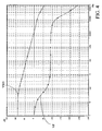
- a Bode diagram of the op-amp 1 is shown in Figure 4. It can be verified that the DC-gain is high as a two poles known system and the phase margin is equal to 85°.
- the op-amp 1 further comprises a RC network compensation circuit 8 providing a compensation via Miller effect.
- the RC network compensation circuit 8 comprises a capacitor Cc and a resistor Rc inserted, in series to each other, between the second internal node B and the output terminal OUT of the op-amp 1.
- the value of the resistor Rc is chosen equal to 1/gm, thus avoiding the introduction of a polo-zero doublet.
- the Applicant has estimated the stability of the op-amp 1 when a large signal is applied to its input terminals IN- and IN+ by using the technique described by PALUMBO et al. in the article: “Feedback Amplifier", Kluwer, Boston, pp.90, 2002 .
- a relative stability can be characterized by the phase margin (PM) in frequency domain and by the so called overshoot of the step response in time domain as a function of separation factor W, which in case of Miller compensation, are given as:
- the op-amp 1 according to the invention have approximately the same relative stability as its linear counterpart.
- the small signal transconductance gm1 of the input transistors changes along with the drain current Id flowing in these transistors and small signal transconductance gmL of the output transistors changes along with the root of the drain current Id flowing therein.
- the separation factor W decreases and, therefore, the phase margin PM is reduced and the stability could be compromised.
- the current feedback factor K2 is chosen small, for instance between 0 and 1, so that the resistance value 1/gm1,2, that is signal dependent, do not change so much.
- the op-amp 1 shown in Figure 3 has been designed in a 0,5 ⁇ m CMOS technology with a 2,4V supply voltage reference.
- Figure 5A shows an output voltage Vout issued by a buffer op-amp 1 for an input voltage Vin being a step of 0,4V when adaptive bias mechanism is not used. It is immediately clear that in this condition the op-amp 1 suffers of slew rate problem and the output voltage Vout does not reach a desired value.
- the small current of the op-amp 1 is in fact unable to drive in linear mode a load capacitor connected to its output terminal OUT and the slew rate is given by the current provided by the tail current generator G 1 divided by the compensation capacitor Cc of the RC network compensation circuit 8.
- Figure 5B shows a same transient simulation for an op-amp 1 using the adaptive bias mechanism (i.e. comprising the adaptive bias block 3).
- the op-amp 1 settles in 1 ⁇ s with a 0,1 % of precision.
- the op-amp 1 comprising a adaptive bias block 3 and a positive feedback network 7 is able to charge a big capacitive load with very low current and a sufficient precision (given by its high DC-gain) is achieved.
- Table 1 resumes the specifications of the op-amp 1 which has been simulated by the Applicant and its measured features.
- Table 1 Technology CMOS 0,5 ⁇ m Power supply 2,4V Cload 10pF Settling time @ 0,1% 1 ⁇ s DC-gain 90dB GBW 1,2MHz Phase Margin 85° Power consumption 24 ⁇ W
- the op-amp 1 is a class AB amplifier suitable to drive large capacitive load in low-voltage low-power applications having a low-power consumption and an adaptive biasing as well as an enhanced DC-gain.
- the impedance seen at the drain terminals of the differential input pair of transistors M1 and M2 is enhanced by the positive feedback network 7 comprising the transistors M5 and M6 so that to enhance the gain of the whole op-amp 1.
- the op-amp 1 comprises a adaptive bias block 3 to regulate its own bias currents and to have a better efficiency in the use of the supply current to charge and discharge an output load.
- the op-amp 1 operates at very low current level, i.e. in a sleeping mode.
- a differential signal Vin is applied to the input terminals IN- and IN+ of the op-amp 1
- the current in the input transistors M1 and M2 is boosted to enhance the slew-rate and achieve a good settling in a required time slot. So, the bias currents are adjusted by sensing an input signal amplitude.
- the proposed op-amp 1 has a slew rate with a great boost so the it is able to manage large input signal in the same manner of small input signal.
- the op-amp 1 solves the problem of the poor DC-gain of the known solution by using a positive feedback structure that enhances the whole op-amp gain up to 90dB (i.e. like a two poles amplifier).
- the proposed op-amp topology could be used in very low voltage applications with a typical supply voltage of 1,2V or even below.
- Useful applications of the op-amp 1 according to the invention are for example in the field of biomedical systems and micro-sensor systems where power dissipation is an important specification for life time battery.
Landscapes
- Engineering & Computer Science (AREA)
- Power Engineering (AREA)
- Amplifiers (AREA)
Priority Applications (2)
| Application Number | Priority Date | Filing Date | Title |
|---|---|---|---|
| EP06011220A EP1863171A1 (fr) | 2006-05-31 | 2006-05-31 | Amplificateur opérationnel en classe AB |
| US11/755,711 US7576610B2 (en) | 2006-05-31 | 2007-05-30 | Operational amplifier of class AB |
Applications Claiming Priority (1)
| Application Number | Priority Date | Filing Date | Title |
|---|---|---|---|
| EP06011220A EP1863171A1 (fr) | 2006-05-31 | 2006-05-31 | Amplificateur opérationnel en classe AB |
Publications (1)
| Publication Number | Publication Date |
|---|---|
| EP1863171A1 true EP1863171A1 (fr) | 2007-12-05 |
Family
ID=37085737
Family Applications (1)
| Application Number | Title | Priority Date | Filing Date |
|---|---|---|---|
| EP06011220A Withdrawn EP1863171A1 (fr) | 2006-05-31 | 2006-05-31 | Amplificateur opérationnel en classe AB |
Country Status (2)
| Country | Link |
|---|---|
| US (1) | US7576610B2 (fr) |
| EP (1) | EP1863171A1 (fr) |
Cited By (3)
| Publication number | Priority date | Publication date | Assignee | Title |
|---|---|---|---|---|
| RU2462812C1 (ru) * | 2011-08-10 | 2012-09-27 | Федеральное государственное бюджетное образовательное учреждение высшего профессионального образования "Южно-Российский государственный университет экономики и сервиса" (ФГБОУ ВПО "ЮРГУЭС") | Операционный усилитель с малым напряжением смещения нуля |
| CN104201999A (zh) * | 2014-09-23 | 2014-12-10 | 无锡华大国奇科技有限公司 | 基于自适应尾电流的跨导运算放大器 |
| CN111510090A (zh) * | 2020-05-19 | 2020-08-07 | 成都微光集电科技有限公司 | 一种高压摆率和宽输出范围的运算放大器 |
Families Citing this family (15)
| Publication number | Priority date | Publication date | Assignee | Title |
|---|---|---|---|---|
| US7999617B2 (en) * | 2006-01-18 | 2011-08-16 | Nxp B.V. | Amplifier circuit |
| JP5355366B2 (ja) * | 2009-12-02 | 2013-11-27 | 株式会社東芝 | 差動増幅回路および無線受信機 |
| US8736357B2 (en) * | 2011-02-28 | 2014-05-27 | Rf Micro Devices, Inc. | Method of generating multiple current sources from a single reference resistor |
| KR101916224B1 (ko) | 2012-03-21 | 2018-11-08 | 삼성전자 주식회사 | 출력 버퍼용 증폭기 및 이를 이용한 신호 처리 장치 |
| US8766726B2 (en) * | 2012-08-10 | 2014-07-01 | Lsi Corporation | Operational amplifier with improved frequency compensation |
| EP2824532B1 (fr) * | 2013-07-10 | 2019-07-03 | Dialog Semiconductor GmbH | Procédé et circuit pour la réduction de gain commandé d'une paire différentielle |
| KR102074230B1 (ko) | 2013-09-23 | 2020-02-06 | 삼성전자주식회사 | 슬루율이 개선된 버퍼 회로 및 이를 포함하는 소스 구동 회로 |
| US10014829B2 (en) * | 2015-12-23 | 2018-07-03 | Omni Design Technologies, Inc. | Non-inverting amplifier circuits |
| CN106026937B (zh) * | 2016-06-06 | 2019-11-26 | 京东方科技集团股份有限公司 | 两级运算放大器 |
| IT201600076746A1 (it) * | 2016-07-21 | 2018-01-21 | St Microelectronics Srl | Circuito comparatore a tempo continuo ad alta velocita' |
| KR102874679B1 (ko) | 2020-10-07 | 2025-10-22 | 삼성전자주식회사 | 증폭기 및 증폭기를 포함하는 전자 장치 |
| US12323115B2 (en) * | 2020-12-29 | 2025-06-03 | Samsung Electronics Co., Ltd. | Operational transconductance amplifier circuit including active inductor |
| US11656642B2 (en) | 2021-02-05 | 2023-05-23 | Analog Devices, Inc. | Slew rate improvement in multistage differential amplifiers for fast transient response linear regulator applications |
| KR102573514B1 (ko) * | 2021-08-25 | 2023-08-31 | 성균관대학교산학협력단 | 적응형 바이어스를 이용한 레일 투 레일 클래스 ab급 버퍼 증폭기 |
| CN119727672B (zh) * | 2024-12-04 | 2025-10-28 | 广东省科学院半导体研究所 | 一种迟滞比较器电路及系统 |
Citations (2)
| Publication number | Priority date | Publication date | Assignee | Title |
|---|---|---|---|---|
| EP0776087A1 (fr) * | 1995-11-24 | 1997-05-28 | Deutsche ITT Industries GmbH | Amplificateur CMOS de transconductance avec polarisation glissante |
| US6600483B1 (en) * | 2000-02-25 | 2003-07-29 | New Japan Radio, Co., Ltd. | Driving circuit |
Family Cites Families (2)
| Publication number | Priority date | Publication date | Assignee | Title |
|---|---|---|---|---|
| US6771126B2 (en) * | 2001-03-30 | 2004-08-03 | Winbond Electronics Corporation | Slew rate enhancement circuit and method |
| JP2005045702A (ja) * | 2003-07-25 | 2005-02-17 | Matsushita Electric Ind Co Ltd | 差動増幅回路および差動増幅回路を搭載したテスト回路 |
-
2006
- 2006-05-31 EP EP06011220A patent/EP1863171A1/fr not_active Withdrawn
-
2007
- 2007-05-30 US US11/755,711 patent/US7576610B2/en active Active
Patent Citations (2)
| Publication number | Priority date | Publication date | Assignee | Title |
|---|---|---|---|---|
| EP0776087A1 (fr) * | 1995-11-24 | 1997-05-28 | Deutsche ITT Industries GmbH | Amplificateur CMOS de transconductance avec polarisation glissante |
| US6600483B1 (en) * | 2000-02-25 | 2003-07-29 | New Japan Radio, Co., Ltd. | Driving circuit |
Non-Patent Citations (1)
| Title |
|---|
| NOCETI FILHO S ET AL: "NEW CMOS OTA FOR FULLY INTEGRATED CONTINUOUS-TIME CIRCUIT APPLICATIONS", ELECTRONICS LETTERS, IEE STEVENAGE, GB, vol. 25, no. 24, 23 November 1989 (1989-11-23), pages 1674 - 1675, XP000075000, ISSN: 0013-5194 * |
Cited By (5)
| Publication number | Priority date | Publication date | Assignee | Title |
|---|---|---|---|---|
| RU2462812C1 (ru) * | 2011-08-10 | 2012-09-27 | Федеральное государственное бюджетное образовательное учреждение высшего профессионального образования "Южно-Российский государственный университет экономики и сервиса" (ФГБОУ ВПО "ЮРГУЭС") | Операционный усилитель с малым напряжением смещения нуля |
| CN104201999A (zh) * | 2014-09-23 | 2014-12-10 | 无锡华大国奇科技有限公司 | 基于自适应尾电流的跨导运算放大器 |
| CN104201999B (zh) * | 2014-09-23 | 2018-04-24 | 无锡华大国奇科技有限公司 | 基于自适应尾电流的跨导运算放大器 |
| CN111510090A (zh) * | 2020-05-19 | 2020-08-07 | 成都微光集电科技有限公司 | 一种高压摆率和宽输出范围的运算放大器 |
| CN111510090B (zh) * | 2020-05-19 | 2023-03-31 | 成都微光集电科技有限公司 | 一种高压摆率和宽输出范围的运算放大器 |
Also Published As
| Publication number | Publication date |
|---|---|
| US7576610B2 (en) | 2009-08-18 |
| US20080001662A1 (en) | 2008-01-03 |
Similar Documents
| Publication | Publication Date | Title |
|---|---|---|
| US7576610B2 (en) | Operational amplifier of class AB | |
| Duisters et al. | A-90-dB THD rail-to-rail input opamp using a new local charge pump in CMOS | |
| Minaei et al. | A new CMOS electronically tunable current conveyor and its application to current-mode filters | |
| US6529070B1 (en) | Low-voltage, broadband operational amplifier | |
| CN113612449B (zh) | 一种运算放大器电路 | |
| Shem-Tov et al. | A high-speed CMOS op-amp design technique using negative Miller capacitance | |
| Khateb et al. | Novel low-voltage low-power high-precision CCII±based on bulk-driven folded cascode OTA | |
| CN1262811A (zh) | 高速和高增益运算放大器 | |
| KR100891221B1 (ko) | 가변이득 증폭기 및 필터회로 | |
| Pennisi | A low-voltage design approach for class AB current-mode circuits | |
| CN118316403A (zh) | 运算放大电路、运算放大器、芯片及电子设备 | |
| US6714079B2 (en) | Differential amplifier with gain substantially independent of temperature | |
| Ferri et al. | Integrated Rail‐to‐Rail Low‐Voltage Low‐Power Enhanced DC‐Gain Fully Differential Operational Transconductance Amplifier | |
| CN110601670A (zh) | 一种麦克风可编程增益放大器集成电路 | |
| US9231540B2 (en) | High performance class AB operational amplifier | |
| JP2007102563A (ja) | 電流発生回路 | |
| Banik et al. | A high-performance low-power two-stage OPAMP realized in 90nm CMOS process for biomedical application | |
| CN215420202U (zh) | 一种运算放大器电路 | |
| KR100662517B1 (ko) | 전류싱크를 이용한 연산 트랜스컨덕턴스 증폭기 | |
| US7453104B2 (en) | Operational amplifier including low DC gain wideband feed forward circuit and high DC gain narrowband gain circuit | |
| Pourashraf et al. | A super class-AB OTA with high output current and no open loop gain degradation | |
| Marano et al. | Step-response optimisation techniques for low-power, high-load, three-stage operational amplifiers driving large capacitive loads | |
| US6542034B2 (en) | Operational amplifier with high gain and symmetrical output-current capability | |
| Lberni et al. | Bulk-driven current conveyor optimization using simulation-based method | |
| Ferri | Low-power adaptive biased integrated amplifiers |
Legal Events
| Date | Code | Title | Description |
|---|---|---|---|
| PUAI | Public reference made under article 153(3) epc to a published international application that has entered the european phase |
Free format text: ORIGINAL CODE: 0009012 |
|
| AK | Designated contracting states |
Kind code of ref document: A1 Designated state(s): AT BE BG CH CY CZ DE DK EE ES FI FR GB GR HU IE IS IT LI LT LU LV MC NL PL PT RO SE SI SK TR |
|
| AX | Request for extension of the european patent |
Extension state: AL BA HR MK YU |
|
| AKX | Designation fees paid | ||
| REG | Reference to a national code |
Ref country code: DE Ref legal event code: 8566 |
|
| STAA | Information on the status of an ep patent application or granted ep patent |
Free format text: STATUS: THE APPLICATION IS DEEMED TO BE WITHDRAWN |
|
| 18D | Application deemed to be withdrawn |
Effective date: 20080606 |