EP1863183B1 - Übertragungsvorrichtung, kommunikationsvorrichtung und mobile drahtlose einheit - Google Patents
Übertragungsvorrichtung, kommunikationsvorrichtung und mobile drahtlose einheit Download PDFInfo
- Publication number
- EP1863183B1 EP1863183B1 EP06729570.9A EP06729570A EP1863183B1 EP 1863183 B1 EP1863183 B1 EP 1863183B1 EP 06729570 A EP06729570 A EP 06729570A EP 1863183 B1 EP1863183 B1 EP 1863183B1
- Authority
- EP
- European Patent Office
- Prior art keywords
- phase
- signal
- section
- modulation signal
- component
- Prior art date
- Legal status (The legal status is an assumption and is not a legal conclusion. Google has not performed a legal analysis and makes no representation as to the accuracy of the status listed.)
- Expired - Lifetime
Links
Images







Classifications
-
- H—ELECTRICITY
- H03—ELECTRONIC CIRCUITRY
- H03F—AMPLIFIERS
- H03F1/00—Details of amplifiers with only discharge tubes, only semiconductor devices or only unspecified devices as amplifying elements
- H03F1/32—Modifications of amplifiers to reduce non-linear distortion
- H03F1/3241—Modifications of amplifiers to reduce non-linear distortion using predistortion circuits
- H03F1/3282—Acting on the phase and the amplitude of the input signal
-
- H—ELECTRICITY
- H03—ELECTRONIC CIRCUITRY
- H03F—AMPLIFIERS
- H03F1/00—Details of amplifiers with only discharge tubes, only semiconductor devices or only unspecified devices as amplifying elements
- H03F1/02—Modifications of amplifiers to raise the efficiency, e.g. gliding Class A stages, use of an auxiliary oscillation
-
- H—ELECTRICITY
- H03—ELECTRONIC CIRCUITRY
- H03F—AMPLIFIERS
- H03F1/00—Details of amplifiers with only discharge tubes, only semiconductor devices or only unspecified devices as amplifying elements
- H03F1/02—Modifications of amplifiers to raise the efficiency, e.g. gliding Class A stages, use of an auxiliary oscillation
- H03F1/0205—Modifications of amplifiers to raise the efficiency, e.g. gliding Class A stages, use of an auxiliary oscillation in transistor amplifiers
-
- H—ELECTRICITY
- H03—ELECTRONIC CIRCUITRY
- H03F—AMPLIFIERS
- H03F1/00—Details of amplifiers with only discharge tubes, only semiconductor devices or only unspecified devices as amplifying elements
- H03F1/32—Modifications of amplifiers to reduce non-linear distortion
-
- H—ELECTRICITY
- H03—ELECTRONIC CIRCUITRY
- H03F—AMPLIFIERS
- H03F1/00—Details of amplifiers with only discharge tubes, only semiconductor devices or only unspecified devices as amplifying elements
- H03F1/32—Modifications of amplifiers to reduce non-linear distortion
- H03F1/3241—Modifications of amplifiers to reduce non-linear distortion using predistortion circuits
- H03F1/3247—Modifications of amplifiers to reduce non-linear distortion using predistortion circuits using feedback acting on predistortion circuits
-
- H—ELECTRICITY
- H03—ELECTRONIC CIRCUITRY
- H03F—AMPLIFIERS
- H03F3/00—Amplifiers with only discharge tubes or only semiconductor devices as amplifying elements
- H03F3/20—Power amplifiers, e.g. Class B amplifiers, Class C amplifiers
- H03F3/24—Power amplifiers, e.g. Class B amplifiers, Class C amplifiers of transmitter output stages
-
- H—ELECTRICITY
- H03—ELECTRONIC CIRCUITRY
- H03F—AMPLIFIERS
- H03F2200/00—Indexing scheme relating to amplifiers
- H03F2200/102—A non-specified detector of a signal envelope being used in an amplifying circuit
-
- H—ELECTRICITY
- H04—ELECTRIC COMMUNICATION TECHNIQUE
- H04B—TRANSMISSION
- H04B1/00—Details of transmission systems, not covered by a single one of groups H04B3/00 - H04B13/00; Details of transmission systems not characterised by the medium used for transmission
- H04B1/02—Transmitters
- H04B1/04—Circuits
- H04B2001/0408—Circuits with power amplifiers
- H04B2001/045—Circuits with power amplifiers with means for improving efficiency
Definitions
- the present invention relates to transmission apparatus carrying out polar modulation so as to generate a vector modulation wave. More particularly, the present invention relates to transmission apparatus synthesizing an amplitude component modulation signal and phase modulation wave so as to generate a vector modulation wave, and communication apparatus and mobile wireless apparatus mounted with this transmission apparatus.
- a power amplifier provided at an output section of transmission apparatus in a wireless communication system requires both low distortion and high efficiency.
- Power amplifiers serving this kind of use are classified into amplifiers using transistors as a current source or using transistors as switches.
- Amplifiers using transistors as a current source may be class A amplifiers, class AB amplifiers, class B amplifiers and class C amplifiers.
- amplifiers using transistors as a switch may be class D amplifiers, class E amplifiers and class F amplifiers.
- class A or class AB linear amplifiers are used in order to amplify envelope fluctuation components in a linear manner, as high-frequency power amplifiers amplifying modulation waves containing envelope fluctuation components.
- the power efficiency of linear amplifiers is inferior compared to non-linear amplifiers such as C class to E class amplifiers.
- a conventional linear amplifier is used as a mobile type wireless apparatus such as a mobile telephone or mobile information terminal using a battery as a power source, because a class A or class AB linear amplifier of large power consumption is used, there is the drawback that usage time is short.
- a conventional linear amplifier is used as base station apparatus for a mobile communication system installed with a plurality of large power transmission apparatus, there is the drawback of inviting increase in size of the transmission apparatus and increased heat generation.
- transmission apparatus having a highly efficient transmission function, equipped with an amplitude phase component extraction section, amplitude signal processing section, phase modulating section, and non-linear amplifying section etc. and carrying out polar modulation are well-known.
- EER envelope Elimination and Restoration
- transmission apparatus configured so that a signal of a constant envelope level is received at a non-linear amplifying section that employs a non-linear amplifier of superior efficiency as a high-frequency amplifier, is proposed as this kind of transmission apparatus.
- apparatus where non-linearity of an envelope signal for a non-linear amplifier is corrected using negative feedback so as to suppress amplitude distortion for example, refer to Non-Patent Document 1 are well known as transmission apparatus.
- FIG.1 is a block diagram showing an example configuration of conventional EER transmission apparatus.
- This EER transmission apparatus employs a configuration comprised of transmission data signal input terminal 11, amplitude phase component extraction section 12, amplitude signal processing section 13, phase modulating section 14, non-linear amplifying section 15 and transmission output terminal 16.
- transmission data signal Si (t) inputted by transmission data signal input terminal 11 is defined by the following equation (1) :
- Si t a t ⁇ exp j ⁇ ⁇ t
- a(t) is an amplitude component modulation signal
- ⁇ (t) is a phase component modulation signal.
- phase modulation wave Sc (t) that is a carrier wave having an angular frequency ⁇ c phase-modulated by phase modulating section 14 using a phase component modulation signal ⁇ (t), is generated and inputted to non-linear amplifying section 15.
- a signal that is power supplyvoltage a (t) of non-linear amplifying section 15 and a phase modulation wave Sc(t) that is an output signal of phase modulating section 804 multiplied together is amplified by a gain G of non-linear amplifying section 15, and outputted as an RF (Radio Frequency) vector modulation wave Srf(t).
- Vector modulation wave Srf(t) at this time is expressed by the following equation (3):
- phase modulation wave Sc(t) inputted to non-linear amplifying section 15 is a phase modulation wave that is a modulation wave of a constant envelope level. It is therefore possible to use a non-linear amplifier of superior efficiency as a high-frequency amplifier, and, as a result, bring about a highly efficient and low distortion transmission apparatus.
- the transmission apparatus shown in FIG. 1 in the event that there is a difference in delay time in the paths taken by the amplitude component and the phase component to reach non-linear amplifying section 15, distortion occurs in the vector modulation wave Srf(t) that is an output signal of non-linear amplifying section 15.
- the signal transmitting the amplitude component is amplitude component modulation signal a(t)
- the signal transmitting the phase component is phase component modulation signal ⁇ (t) or phase modulation wave Sc(t)
- FIG.2 is a characteristic diagram showing the relationship between the frequency and amplitude of a vector modulation wave of the transmission apparatus shown in FIG.1 , with FIG.2A showing the case where there is no difference in delay time, and FIG.2B showing the case where there is a difference in delay time.
- FIG.2 is a graph showing a frequency spectrum for vector frequency Srf(t) that is an output signal of non-linear amplifying section 15 of the transmission apparatus of FIG.1 . If there is a difference in delay time in the paths the amplitude component and phase component take to reach non-linear amplifying section 15, as shown in FIG.2A , broadening of the frequency spectrum cannot be seen.
- FIG.3 is a block diagram showing a configuration for Conventional EER transmission apparatus such as Japanese Patent Document 1 etc. for improving distortion of vector modulation waves.
- FIG.3 is a block diagram showing a configuration for transmission apparatus equipped with a function for correcting a difference in delay time occurring in paths the amplitude component and phase component take to reach non-linear power amplifying section 28.
- This transmission apparatus is comprised of transmission data input terminal 21, polar coordinate component modulation signal generating section 22 forming a modulation signal of an amplitude component and a phase component, timing correcting section 23, band-limiting filters 24 and 25, amplitude controlling section 26, phase modulating section 27, power amplifying section 28, transmission output terminal 29, phase angle measuring section 30, amplitude measuring section 31, and correction data storing section 32.
- this transmission apparatus selects correction data according to results of referring to an amplitude component and phase component of vector modulation wave Srf(t) that is the output signal of power amplifying section 28, and corrects and controls amplitude controlling section 26 and phase modulating section 27.
- the difference in delay time between the amplitude component and the phase component is known by again extracting and referring to the amplitude component and the phase component from the vector modulation wave Srf (t) and subjecting amplitude controlling section 26 and phase modulating section 27 to control corresponding to the correction of this difference.
- timing correcting section 23 performs correction and control, and it is possible to directly adjust the time relationship between the amplitude component modulation signal a(t) and the phase component modulation signal ⁇ (t).
- Patent Document 1 US Patent No.6,366,177B1
- Non-Patent Document 1 Peter B. Kenington, "IGH-LINEARITY RF AMPLIFIER DESIGN," volume 1, ARTECH HOUSE, INC., 2000, p. 426-443 JP 2004 356 835 A relates to a transmission apparatus systhesizing an amplitude component and a phase component using polar modulation.
- phase angle measuring section 30 It is necessary for phase angle measuring section 30 to function as a frequency discriminator that is a demodulator for a PM (Phase Modulation) modulation wave and an FM (Frequency Modulation) wave and is comprised of, for example, a pulse count detector circuit and a low pass filter circuit etc.
- amplitude measuring section 31 it is necessary for amplitude measuring section 31 to function as an envelope detector that is a demodulator for AM (Amplitude Modulation) modulation waves and is comprised of, for example, a diode detector circuit and a low pass filter circuit, etc. Because of this, differences occur in measurement processing time due to differences in the circuit configuration of both circuits and it is therefore not possible to measure delay time in a precise manner.
- phase angle measuring section 30 and amplitude measuring section 31. It is therefore not possible to accurately measure differences in delay time between the amplitude component and the phase component. Because of this, it is difficult to reduce distortion of vector modulation wave Srf(t) that is the output of power amplifying section 28 to a sufficiently small level.
- transmission apparatus comprises the features of claim 1.
- a method embodiment of the transmission apparatus of the the polar coordinate component modulation signal generating section is comprised of: an in-phase/quadrature component modulation signal generating section that forms the in-phase component modulation signal and the quadrature component modulation signal; and a coordinate converting section that forms an amplitude component modulation signal and phase component modulation signal based on the in-phase component modulation signal and the quadrature component modulation signal, the in-phase/quadrature component modulation signal generating section forms a first sine wave signal having a first frequency f1 and a first phase angle p1 as the in-phase component modulation signal and a second sine wave signal having a frequency that is the same as the first frequency of f1 and a second phase angle p2 where the difference with the first phase angle p1 is not an integer multiple of ninety degrees, as the quadrature component modulation signal, the band filtering section extracts a signal of a frequency component that is the second frequency f2 expressed by a value that is n times the first frequency f
- a signal is generated by the polar coordinate component modulation signal generating section in such a manner that a distortion component appears at a frequency component that is the second frequency f2 expressed by a value that is n (where n is an odd number of three or more) times the first frequency f1 in the event that a difference in delay time occurs in the paths the amplitude component modulation signal and phase component take to reach the amplifying section.
- the second frequency f2 is then extracted by the band filtering section.
- the controlling section also then controls the delay time adjusting section in such a manner that the level of the output signal of the band filtering section becomes small. It is therefore possible to reliably correct and control the delay time difference between the amplitude component modulation signal and the phase component modulation signal in the event of differences in delay time between the paths the amplitude component modulation signal and the phase component take to reach the amplifying section.
- the polar coordinate component modulation signal generating section is provided with: an in-phase/quadrature component modulation signal generating section that forms the in-phase component modulation signal and the quadrature component modulation signal; and a coordinate converting section that forms an amplitude component modulation signal and phase component modulation signal based on the in-phase component modulation signal and the quadrature component modulation signal, the in-phase/quadrature component modulation signal generating section adds a first sine wave signal of a first frequency f1 and having a first phase angle p1 and a second sine wave signal of the second frequency f2 having the first phase angle p1 and forms a signal as the in-phase component modulation signal, and adds a third sine wave signal of the same frequency as the first frequency f1 and having a second phase angle p2 where a difference with the first phase angle p1 is an odd multiple of ninety degrees, and a fourth sine wave signal having the same frequency as the second frequency f2 and the second
- a signal is generated by the polar coordinate component modulation signal generating section in such a manner that a distortion component appears at a frequency component that is a third frequency f3 expressed by the sum of a value that is n times the first frequency f1 and a value that is (n+1) times the second frequency f2 in the event that a difference in delay time occurs in the paths the amplitude component modulation signal and phase component take to reach the amplifying section.
- the third frequency f3 is then extracted by the band filtering section.
- the controlling section also then controls the delay time adjusting section in such a manner that the level of the output signal of the band filtering section becomes small. It is therefore possible to reliably correct and control the delay time difference between the amplitude component modulation signal and the phase component modulation signal in the event of differences in time delay between the paths the amplitude component modulation signal and the phase component take to reach the amplifying section.
- communication apparatus or mobile wireless apparatus mounted with this transmission apparatus is capable of providing apparatus that can transmit high-quality signals with little distortion component.
- delay time differences between the amplitude component modulation signal and the phase component modulation signal are corrected and controlled by detecting distortion of a modulation wave using synchronously demodulating, so that it is possible to reduce the distortion of the vector modulation wave down to a sufficiently small level.
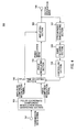
- FIG.4 is a block diagram showing a configuration for a transmission apparatus of a first embodiment of the present invention.
- Transmission apparatus 100 shown in FIG.4 is comprised of transmission data signal input terminal 101 inputting a transmission data signal, polar coordinate component modulation signal generating section 102 forming an amplitude component modulation signal and a phase component modulation signal based on an inputted transmission data signal, delay time adjusting section 103 changing the delay time of an amplitude component modulation signal and a phase component modulation signal, phase modulating section 104 forming a phase modulation wave where a carrier wave is phase-modulated by the phase component modulation signal, amplifying section 105 receiving as input the phase modulation wave at a signal input terminal of transmission apparatus 100, with the amplitude component modulation signal applied to a power supply voltage terminal of transmission apparatus 100, forming a vector modulation wave where the phase modulation wave is amplitude-modulated by the amplitude component modulation signal, transmission output terminal 106 outputting a vector modulation wave, synchronous demodulating section
- Polar coordinate component modulation signal generating section 102 forms an amplitude component modulation signal and phase component modulation signal based on a transmission data signal inputted by transmission data signal input terminal 101, and supplies the amplitude component modulation signal to amplifying section 105 via delay time adjusting section 103 as a power supply voltage.
- the phase component modulation signal is inputted to phase modulating section 104 via delay time adjusting section 103.
- phase modulating section 104 forms a phase modulation wave by subjecting a carrier wave to phase modulation using a phase component modulation signal and transmits this phase modulation wave to amplifying section 105.
- Amplifying section 105 is a high-frequency amplifier equipped with a semiconductor amplifier element. At this amplifying section 105, a phase modulation wave from phase modulating section 104 and an amplitude component modulation signal that is the power supply voltage are multiplied together, and an RF signal amplified by a predetermined gain is outputted as a vector modulation signal from transmission output terminal 106. At this time, amplifying section 105 is capable of carrying out non-linear amplification of superior efficiency because the input signal is a phase modulation wave of a constant envelope level.
- Synchronous demodulating section 107 synchronously demodulates the vector modulation wave outputted by amplifying section 105, and forms a synchronous demodulation signal. Namely, synchronous demodulating section 107 forms a synchronous demodulation signal frequency-converted to the baseband by multiplying the vector modulation wave outputted by amplifying section 105 and a localized oscillation signal (local signal) having the same frequency as the center frequency of the vector modulation wave using a mixer circuit, and transmits this synchronous demodulation signal to band filtering section 108.
- localized oscillation signal local signal
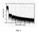
- FIG.5 is a characteristic diagram showing the frequency spectrum of a synchronous demodulation signal outputted by synchronous demodulating section 107 in the transmission apparatus of FIG.4 , where the horizontal axis represents frequency (MHz) and the vertical axis represents amplitude (dB) of the synchronous demodulation signal. Namely, when there is a difference in delay time for the paths that the amplitude component and the phase component take to reach amplifying section 105, as with the case where the vector modulation wave shown in FIG.2 described previously, the characteristic of the synchronous demodulation signal becomes as shown in FIG. 5 .
- the synchronous demodulation signal outputted from synchronous demodulating section 107 maintains information about distortions (broadening of the frequency spectrum shown in FIG.5 ) occurring in the vector modulation wave outputted by amplifying section 105.
- band filtering section 108 extracts a signal of the frequency component for distortion from a synchronous demodulation signal outputted by synchronous demodulating section 107
- controlling section 109 refers to the distortion component signal extracted by band filtering section 108 and controls delay time adjusting section 103 in such a manner that the signal level of this distortion component becomes small, and the delay time difference between the amplitude component modulation signal and the phase component modulation signal is adjusted.
- the purpose of the delay time adjustment is achieved by, for example, controlling section 109 controlling delay time adjusting section 103 and storing the value for the delay time with which the signal level of the distortion component extracted by band filtering section 108 is a minimum in memory as necessary while changing the delay time of the amplitude component modulation signal a little at a time, with the stored value then being set as a value for the delay time provided to delay time adjusting section 103 at the time of completion of change in the delay time within a certain fixed range.
- amplifying section 105 generates a vector modulation wave based on the amplitude component modulation signal and phase modulation wave, but in the event that there is a difference in delay time in the paths the amplitude component and the phase component take to reach amplifying section 105, synchronous demodulating section 107 detects the vector modulation wave, forms a synchronous demodulation signal, and transmits this to band filtering section 108.
- band filtering section 108 extracts the signal of the frequency component of distortion from the synchronous demodulation signal inputted by synchronous demodulating section 107
- controlling section 109 refers to the distortion component signal extracted by band filtering section 108 and controls the delay time adjusting section 103 in such a manner that the signal level of this distortion component becomes small, and the delay time difference between the amplitude component modulation signal and the phase modulation signal is adjusted so as to reduce distortion in the modulation wave.
- the transmission apparatus of the first embodiment of the present invention it is possible to detect distortion of a modulation wave occurring as a result of delay time differences between the amplitude component and the phase component by synchronously demodulating a vector modulation wave without separating and extracting the amplitude component and the phase component from the vector modulation wave, and delay time differences between the amplitude component modulation signal and the phase component modulation signal are corrected and controlled based on these detection results, so that it is possible to reduce the distortion of the vector modulation wave down to a sufficiently small level.
- FIG.6 is a block diagram showing a configuration for transmission apparatus of this embodiment.
- Polar coordinate component modulation signal generating section 310 of transmission apparatus 300 of this embodiment is comprised of in-phase/quadrature component modulation signal generating section 311 and polar coordinate converting section 302. Further, in-phase/quadrature component modulation signal generating section 311 has sine-wave generating section 301 and phase shifting section 303.
- in-phase/quadrature component modulation signal generating section 311 forms a first sine wave signal, as an in-phase component modulation signal, having a first frequency f1 and a first phase angle p1, and a second sine wave signal, as a quadrature component modulation signal, having a frequency that is the same as the first frequency of f1 and a second phase angle p2 where the difference with the first phase angle p1 is not an integer multiple of ninety degrees, using sine-wave generating section 301 and phase shifting section 303.
- in-phase/quadrature component modulation signal generating section 311 sends the first sine wave of frequency f1 generated by sine wave generating section 301 to coordinate converting section 302 as an in-phase component modulation signal, and the sine wave of frequency f1 generated by sine-wave generating section 301 is phase-shifted by phase shifting section 303 and is sent to coordinate converting section 302 as the quadrature component modulation signal.
- phase shifting section 303 shifts the phase of the sine wave in such a manner that the difference between the phase angle p2 of the quadrature component modulation signal and the phase angle p1 of the in-phase component modulation signal does not become an integer multiple of ninety degrees.
- Coordinate converting section 302 forms an amplitude component modulation signal and a phase component modulation signal from the in-phase component modulation signal and the quadrature component modulation signal, and these are sent to delay time adjusting section 103.
- the in-phase component modulation signal I (t) and quadrature component modulation signal Q(t) inputted to coordinate converting section 302 are typically referred to as the I (In-phase) component modulation signal and Q (Quadrature) component modulation signal.
- the in-phase component modulation signal I(t) and quadrature component modulation signal Q(t) are signals expressing transmission data signal Si(t) in the form of Cartesian coordinates.
- a Cartesian coordinate is also referred to as an IQ coordinate or XY coordinate.
- Coordinate converting section 302 forms amplitude component modulation signal a(t) and phase component modulation signal ⁇ (t) expressed using polar coordinates from in-phase component modulation signal I(t) and quadrature component modulation signal Q(t) expressed in the form of Cartesian coordinates.
- amplitude component modulation signal a(t) is expressed by the following equation (4)
- phase component modulation signal ⁇ (t) is expressed by the following equation (5).
- In-phase/quadrature component modulation signal generating section 311 forms a signal expressed by the following equation (6) as a sine wave signal having a frequency f1 and phase angle p1 as an in-phase component modulation signal I(t).
- a signal expressed by the following equation (7) is formed as a sine wave signal having frequency f1 and phase angle p2 as a quadrature component modulation signal Q(t).
- I t sin 2 ⁇ ⁇ ⁇ f ⁇ 1 ⁇ t + p ⁇ 1
- Q t sin 2 ⁇ ⁇ ⁇ f ⁇ 1 ⁇ t + p ⁇ 2
- phase angle p1 and phase angle p2 are such that the difference between their values does not have a value of an integer multiple of ninety degrees.
- the difference between phase angle p1 and phase angle p2 is, for example, ninety degrees
- the amplitude component modulation signal a(t) outputted from coordinate converting section 302 becomes a fixed value. Therefore, even if the time relationship between amplitude component modulation signal a(t) and phase component modulation signal ⁇ (t) changes, the phase modulation wave is multiplied with the amplitude component modulation signal that is a fixed value at amplifying section 105, so that the vector modulation wave outputted by amplifying section 105 does not change and, as a result, distortion does not occur. Taking this into consideration, in this embodiment, it is ensured that the difference between phase angle p1 and phase angle p2 does not become an integer multiple of ninety degrees.
- FIG.7 is a characteristic diagram illustrating the operation of polar coordinate component modulation signal generating section 310 of this embodiment.
- FIG.7 is a characteristic diagram illustrating characteristics of transmission apparatus of a second embodiment of the present invention, with the conditions that are different for this second embodiment of the present invention being the difference of the phase angle p1 and phase angle p2, i.e. a characteristic diagram showing in-phase component modulation signal I(t) and quadrature component modulation signal Q(t) in the event that (p2 - p1) is, for example, ninety degrees.
- FIG.7A expresses the time [ ⁇ S] on the horizontal axis, the voltage (V) of the in-phase component modulation signal I (t) and quadrature component modulation signal Q(t) on the vertical axis, and shows a time waveform for I (t) and Q(t).
- FIG.7B shows voltage (V) of in-phase component modulation signal I (t) on the horizontal axis, shows voltage (V) of quadrature component modulation signal Q(t) on the vertical axis, and shows a constellation depicted with I(t) and Q(t).
- the characteristic diagram of FIG.7B is also referred to as a signal space diagram.
- amplitude component modulation signal a(t) corresponds to the distance between the origin (center of the circle) and coordinates (I(t), Q(t)) in the constellation as in FIG.7B .
- a locus of coordinates (I(t), Q(t)) where the phase difference of in-phase component modulation signal I(t) and quadrature component modulation signal Q(t) is ninety degrees depicts a circle, and amplitude component modulation signal a (t) is usually a fixed value.
- an in-phase component modulation signal and a quadrature component modulation signal are formed by sine-wave generating section 301 and phase shifting section 303 in such a manner that the difference of the phase angle p1 and phase angle p2 does not become an integral multiple of ninety degrees.
- FIG.8 is a characteristic diagram illustrating the operation of polar coordinate component modulation signal generating section 310 of this embodiment.
- FIG.8 is a characteristic diagram showing in-phase component modulation signal I(t) and quadrature component modulation signal Q(t) in the event that in-phase/quadrature component modulation signal generating section 311 of this embodiment is such that the difference of phase angle p1 and phase angle p2 is not an integer multiple of ninety degrees.
- FIG.8 shows the case where the difference of phase angle p1 and phase angle p2 i.e. (p2 - p1) is, for example, sixty degrees.
- FIG.8A expresses the time [ ⁇ S] on the horizontal axis, the voltage (V) of I(t) and Q(t) on the vertical axis, and shows a time waveform for I (t) and Q (t). Further, FIG.8B shows the voltage (V) of I(t) on the horizontal axis, and the voltage (V) of Q(t) on the vertical axis, and shows a constellation depicted with I(t) and Q(t).
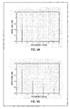
- FIG.9 is a characteristic diagram illustrating an operation of synchronous demodulating section 107 of transmission apparatus 300 of this embodiment. Specifically, FIG.9 is a characteristic diagram showing a frequency spectrum of a synchronous demodulation signal that is the output signal of synchronous demodulating section 107.
- FIG.9A When there is no difference in the delay time for the paths the amplitude component modulation signal and the phase component take to reach amplifying section 105, as shown in FIG.9A , only the 1MHz component appears, and a distortion component does not occur. However, when there is a difference in delay time in the paths the amplitude component modulation signal and the phase component take to reach amplifying section 105, as shown in FIG.
- a distortion component occurs at 3MHz, 5MHz, and 7MHz with respect to the sine wave of frequency of 1MHz generated by sine-wave generating section 301.
- the value of these distortion frequency component have values that are odd-numbered multiples of three or more with respect to the frequency f1 of the sine wave generated by sine-wave generating section 301.
- Band filtering section 108 extracts a signal of a frequency component that is a frequency f2 expressed by a value that is n times the frequency f1.
- the value of n may be any one value of the values that are odd numbers of three or more.
- Band filtering section 108 is configured as a so-called band-pass filter whereby a component of unit frequency f2 that is one of a frequency component of distortion occurring in a synchronous demodulation signal outputted from synchronous demodulating section 107 is extracted and other noise components and signal components of frequency f1 are suppressed.
- Other distortion components and the signal component of frequency f1 exist in frequencies isolated from the component for frequency f2, and suppression to a sufficiently low level is possible. It is therefore possible to precisely extract only the distortion component of frequency f2.
- in-phase/quadrature component modulation signal generating section 311 generates a first sine wave signal having a first frequency f1 and having a first phase angle p1 being formed as an in-phase component modulation signal, and a second sine wave signal having a second phase angle p2 with the same frequency as the first frequency f1 as a quadrature component modulation signal, where the difference with the first phase angle p1 is not an integer multiple of ninety degrees, and band filtering section 108 extracts a signal of a frequency component that is the second frequency f2 expressed by a value that is n times (where n is an odd number of three or more) the first frequency f1, so that it is possible to detect distortion of the modulation wave in a precise manner and reduce distortion to a sufficiently small level.
- FIG.10 shows a configuration for transmission apparatus of the present embodiment.
- Transmission apparatus 400 of this embodiment is different from transmission apparatus 300 of the second embodiment shown in FIG. 6 in that rather than having sine-wave generating section 301 and phase shifting section 303, in-phase/quadrature component modulation signal generating section 411 has sine wave generating sections 401 and 402, phase shifting sections 403 and 404, and adding sections 405 and 406.
- Sine wave generating section 401 generates a sine wave of frequency f1 and transmits this to phase shifting section 403 and adding section 405.
- Sine wave generating section 402 generates a sine wave of frequency f2 that is different from frequency f1 and transmits this to phase shifting section 404 and adding section 405.
- Phase shifting section 403 shifts and outputs the phase of the inputted sine wave in such a manner that the difference in the phase angle of the inputted sine wave and the outputted sine wave becomes an odd multiple of ninety degrees.
- phase shifting section 404 shifts and outputs the phase of the inputted sine wave in such a manner that the difference in the phase angle of the inputted sine wave and the outputted sine wave becomes an odd multiple of ninety degrees.
- a signal that is the sum of a sine wave signal having a frequency f1 and phase angle p1 and a sine wave signal having frequency f2 and phase angle p1 is outputted from adding section 405 as an in-phase component modulation signal.
- a signal that is the sum of a sine wave signal having a frequency f1 and a phase angle p2 of with a difference with phase angle p1 that is an odd multiple of ninety degrees and a sine wave signal having a frequency f2 and a phase angle p2 is outputted from adding section 406 as a quadrature component modulation signal.
- in-phase/quadrature component modulation signal generating section 411 forms a signal expressed by the following equation (8) as an in-phase component modulation signal I(t).
- I t a ⁇ 1 ⁇ sin 2 ⁇ ⁇ ⁇ f ⁇ 1 ⁇ t + p ⁇ 1 + a ⁇ 2 ⁇ sin 2 ⁇ ⁇ ⁇ f ⁇ 2 ⁇ t + p ⁇ 1
- in-phase/quadrature component modulation signal generating section 411 forms a signal expressed by the following equation (9) as a quadrature component modulation signal Q(t).
- phase angle p1 and phase angle p2 are such that the difference between these values becomes a value of ninety degrees.
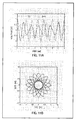
- FIG.11 is a characteristic diagram illustrating the operation of polar coordinate component modulation signal generating section 410 of this embodiment.
- FIG.11 is a graph showing in-phase component modulation signal I(t) and quadrature component modulation signal Q(t).
- FIG.11A expresses the time [ ⁇ S] on the horizontal axis, the voltage of I (t) and Q (t) on the vertical axis, and shows a time waveform for I(t) and Q(t).
- FIG. 11B shows the voltage (V) of I(t) on the horizontal axis, the voltage (V) of Q(t) on the vertical axis, and shows a constellation depicted with I(t) and Q(t).
- Amplitude component modulation signal a(t) corresponds to the distance between the origin and coordinates (I(t), Q(t)) in the constellation of FIG. 11B .
- the value for the amplitude component modulation signal a(t) changes substantially with time because the locus of coordinates (I(t), Q(t)) goes far away from the origin and approaches close to the origin.
- the envelope level of the vector modulation wave that is the output signal of amplifying section 105 changes substantially.
- AM-AM characteristics gain characteristics changing according to envelope level
- AM-PM characteristics phase characteristics changing according to envelope level
- a transmission data signal for the case where information is to be transmitted by transmission apparatus is random and, under such operating conditions, the vector modulation wave that is the output signal of the transmission apparatus also behaves in a randommanner, and the envelope level changes substantially.
- the value of amplitude component modulation signal a(t) outputted by polar coordinate component modulation signal generating section 410 changes substantially with time
- the envelope level of the vector modulation wave outputted from amplifying section 105 therefore also changes substantially
- the normal operation conditions of the transmission apparatus exhibit behavior close to the following conditions.
- amplifying section 105 has pass characteristics such as AM-AM characteristics or AM-PM characteristics
- pass characteristics that are close to being under normal operating conditions of the transmission apparatus are maintained at amplifying section 105.
- distortion occurring in a vector modulation wave outputted from amplifying section 105 is observed as distortion close to that occurring under normal operating conditions of the transmission apparatus.
- FIG.12 is a characteristic diagram illustrating an operation of synchronous demodulating section 107 of transmission apparatus 400 of this embodiment. Specifically, FIG.12 is a graph showing a frequency spectrum of a synchronous demodulation signal that is the output signal of synchronous demodulating section 107. As shown in FIG.12A , when there is no difference in delay time in the paths the amplitude component and the phase component take to reach amplifying section 105, a distortion component does not occur, as shown in FIG. 12B , and, when there is a difference in delay time for the paths taken by the amplitude component modulation signal and the phase modulation wave to reach amplifying section 105, a distortion component occurs.
- the value of the frequency component of this distortion is a value expressed by the sum of a value that is n times the frequency f1 of a sine wave generated by sine wave generating section 401 and a value that is (n+1) times the frequency f2 of the sine wave generated by sine wave generating section 402.
- the magnitude relationship of f1 and f2 is not particularly specified.
- Band filtering section 412 extracts a signal of a frequency component that is a frequency f3 expressed by the sum of a value that is n times frequency f1 and a value that is (n+1) times frequency f2.
- the value of n may be any one value of values that are integers of one or more.
- in-phase/quadrature component modulation signal generating section 411 adds a first sine wave signal having a first frequency f1 and a first phase angle p1 and a second sine wave signal having a second frequency f2 and a first phase angle p1 and forms a signal as an in-phase component modulation signal, and adds a third sine wave signal having the same frequency as the first frequency f1 and second phase angle p2 where the difference with the first phase angle p1 is an odd multiple of ninety degrees and a fourth sine wave signal having the same frequency as the second frequency f2 and having a second phase angle p2 and forms a signals as a quadrature component modulation signal.
- a signal of a frequency component that is the third frequency f3 expressed by the sum of a value that is n times (where n is an integer of one or more) the first frequency f1 and a value that is (n+1) times the second frequency f2 is then extracted by band filtering section 412. In this way, distortion of the modulation wave is detected with good precision and can be reduced to a sufficiently small level.
- in-phase/quadrature component modulation signal generating section 411 employs a configuration having a sine wave generating section, phase shifting section and adding section, but a configuration with the sine wave generating section, phase shifting section and adding section is by no means essential. Even if the in-phase/quadrature component modulation signal generating section is not provided with a sine wave generating section, phase shifting section, and adding section, provided that a configuration whereby it is possible to form an in-phase component modulation signal and quadrature component modulation signal as shown in equation (8) and equation (9) in the sine wave phase shifting and addition is provided, it is possible to obtain the same results regardless of the configuration.
- Transmission apparatus 500 of this embodiment differs from transmission apparatus 100 of the first embodiment shown in FIG.1 in that synchronous demodulating section 107 is omitted, and the configuration of band filtering section 501 and controlling section 502 is different from band filtering section 108 and controlling section 109.
- delay time adjusting section 103 is controlled in such a manner as to make the signal level of a distortion component small by extracting the distortion component of the vector modulation wave from the synchronous demodulation signal by band filtering section 108 after frequency conversion of an RF band vector modulation wave to a baseband by synchronous demodulating section 107 and controlling section 109 referring to the signal of the distortion component extracted by band filtering section 108.
- transmission apparatus 500 of this embodiment controls delay time adjusting section 103 in such a manner that an RF band vector modulation signal is directly inputted to band filtering section 501, a distortion component of the vector modulation wave is directly extracted by band filtering section 501, and controlling section 502 refers to a signal of a distortion component extracted by band filtering section 502 and ensures that the signal level of the distortion component becomes small.
- band filtering section 501 is comprised of a high-frequency band pass filter through which frequencies of the RF band vector modulation wave that are in the vicinity of the carrier wave frequency are made to pass. Specifically, in the event of inputting the RF band vector modulation wave as shown, for example, in FIG.2B , band filtering section 501 allows frequencies of 1.935GHz to 1.945 GHz or 1.955GHz to 1.965GHz (i.e. frequencies in the vicinity of the carrier frequency of 1.95GHz) to pass. Namely, in the event that there is a difference in delay time in the paths to reach amplifying section 105, band filtering section 501 allows frequency components of portions where distortions of the vector modulation wave appear as broadening of the frequency spectrum to pass.
- Controlling section 502 observes broadening of the frequency spectrum of the vector modulation wave inputted fromband filtering section 501 and adjusts delay time adjusting section 103 in such a manner that broadening of the frequency spectrum becomes small. Namely, the vector modulation wave as shown in FIG.2B adjusts delay time adjusting section 103 in such a manner as to give the kind of vector modulation wave shown in FIG.2A .
- band filtering section 501 extracting a signal of a specific frequency component of the vector modulation wave formed by amplifying section 105 and controlling section 502 controlling delay time adjusting section 103 in such a manner that broadening of the frequency spectrum of the vector modulation wave extracted by band filtering section 501 becomes small, it is possible to reduce distortion of a vector modulation wave to a sufficiently small amount without dividing and extracting an amplitude component and phase component from the vector modulation wave.
- Transmission apparatus 600 of this embodiment differs from transmission apparatus 300 of the second embodiment shown in FIG.6 in that synchronous demodulating section 107 is omitted, and the configuration of band filtering section 601 and controlling section 602 is different from band filtering section 108 and controlling section 109.
- FIG.15 is a characteristic diagram showing a frequency spectrogram of the vector frequency that is the output signal of amplifying section 105.
- the horizontal axis shows the difference between the vector modulation wave and the carrier frequency (center frequency) where 0MHz corresponds to the carrier frequency.
- the difference with the carrier wave frequency appears as a distortion component at 3MHz, 5MHz, and 7MHz with respect to the frequency of 1MHz of the sine wave generated by sine-wave generating section 301.
- the difference with the carrier frequency for the value of this distortion frequency component has values that are odd-numbered multiples of three or more with respect to the frequency f1 of the sine wave generated by sine-wave generating section 301.
- band filtering section 601 of transmission apparatus 600 is configured to extract a signal of a frequency component that is f2 with which the difference with the carrier frequency is represented by a value that is n times the frequency f1 (frequency of a sine wave generated by sine-wave generating section 301).
- n is any one value of the values that are odd numbers of three or more.
- band filtering section 601 may be configured from a band pass filter whereby a component with which the difference with the carrier frequency is f2 that is one of the frequency components occurring in the vector modulation wave outputted by amplifying section 105 is extracted, and a signal component with which the difference with another distortion component or the carrier frequency is f1 is suppressed.
- a signal component where the difference with another distortion component and a carrier frequency is f1 exists in a frequency isolated from the component where the difference with the carrier frequency is f2 and suppression down to a sufficiently low level can be achieved.
- the band filtering section 601 is therefore capable of precisely extracting only the distortion component with which the difference with the carrier frequency is f2.
- the magnitude relationship of the carrier frequency and f2 is not particularly specified.
- Controlling section 602 observes the differences with the carrier frequency inputted from band filtering section 601 and adjusts delay time adjusting section 103 in such a manner that the level of the component for f2 becomes small.
- band filtering section 601 extracting from the vector modulation wave formed by amplifying section 105 a signal of a frequency component of f2 with which a difference with a carrier frequency is expressed by a value that is n (any one value of values that are odd numbers of three or more) times the frequency f1 (frequency of a sine wave generated by sine wave generating section 301), and a controlling section 602 observing a component with a difference with the carrier wave frequency extracted by band filtering section 601 of f2 and adjusting delay time adjusting section
- Transmission apparatus 700 of this embodiment differs from transmission apparatus 400 of the third embodiment shown in FIG.10 in that synchronous demodulating section 107 is omitted, and the configuration of band filtering section 701 and controlling section 702 is different from band filtering section 108 and controlling section 109.
- FIG.17 is a characteristic diagram showing a frequency spectrogram of the vector frequency that is the output signal of amplifying section 105.
- the horizontal axis shows the difference between the vector modulation wave and the carrier frequency (center frequency) where 0MHz corresponds to the carrier frequency.
- the value of the frequency component of this distortion is such that a difference with the carrier frequency is a value expressed by the sum of a value that is n times the frequency f1 of a sine wave generated by sine wave generating section 401 and a value that is (n+1) times the frequency f2 generated by sine wave generating section 402.
- n is an integer of one or more.
- Band filtering section 701 of transmission apparatus 700 is configured in such a manner as to extract a signal of a frequency component of frequency f3 expressing a difference with the carrier frequency that is the sum of a value that is n times the frequency f1 (frequency of the sine wave generated by sine wave generating section 401) and a value that is (n+1) times the frequency f2 (frequency of the sine wave generated by sine wave generating section 402).
- the value of n is any one value of integers of one or more.
- the magnitude relationship of f1 and f2 and the magnitude relationship of the carrier frequency and f3 are not particularly specified.
- Controlling section 702 observes the frequency component of frequency f3 inputted from band filtering section 701 and adjusts delay time adjusting section 103 in such a manner that the level of the component for f3 becomes small.
- band filtering section 701 extracting from the vector modulation wave formed by amplifying section 105 a signal of a frequency component of frequency f3 with which the difference with a carrier frequency is expressed by the sum of a value that is n times (where n is an integer of one or more) the frequency f
- transmission apparatus of each of the embodiments described above on communication apparatus or mobile wireless apparatus. Accordingly, as it is possible to appropriately correct a delay time difference between an amplitude component modulation signal and a phase component modulation signal at transmission apparatus, communication apparatus or mobile wireless apparatus mounted with this transmission apparatus is capable of providing apparatus that can transmit high-quality signals with little distortion component.
- the transmission apparatus of the present invention can reduce the distortion of the vector modulation wave synthesized an amplitude component and a phase component down to a sufficiently small level, and is widely applicable to a communication apparatus, a mobile wireless apparatus and so on.
Landscapes
- Engineering & Computer Science (AREA)
- Power Engineering (AREA)
- Physics & Mathematics (AREA)
- Nonlinear Science (AREA)
- Transmitters (AREA)
- Amplifiers (AREA)
- Digital Transmission Methods That Use Modulated Carrier Waves (AREA)
Claims (4)
- Sendevorrichtung (100, 300, 400, 500, 600, 700), die eine Amplituden-Komponente und eine Phasen-Komponente unter Verwendung von Polarmodulation zusammensetzt und eine Vektormodulations-Welle erzeugt und sendet, wobei die Sendevorrichtung umfasst:einen Abschnitt (102, 310, 410) zum Erzeugen von Polarkoordinatenkomponenten-Modulationssignalen, der ein Amplitudenkomponenten-Modulationssignal sowie ein Phasenkomponenten-Modulationssignal auf Basis eines Eingangssignals ausbildet;einen Abschnitt (103) zum Anpassen einer Verzögerungszeit, der eine Verzögerungszeit-Differenz zwischen dem Amplitudenkomponenten-Modulationssignal und dem Phasenkomponenten-Modulationssignal ändert;einen Phasenmodulations-Abschnitt (104), der eine Phasenmodulations-Welle ausbildet, bei der eine Trägerwelle durch das Phasenkomponenten-Modulationssignal phasenmoduliert wird;einen Verstärkungs-Abschnitt (105), der als Eingang die Phasenmodulations-Welle an einem Signaleingangsanschluss der Sendevorrichtung empfängt, wobei das Amplitudenkomponenten-Modulationssignal an einen Stromversorgungs-Spannungsanschluss der Sendevorrichtung angelegt wird, und der eine Vektormodulations-Welle ausbildet, bei der die Phasenmodulations-Welle durch das Amplitudenkomponenten-Modulationssignal amplitudenmoduliert wird;einen Synchrondemodulations-Abschnitt (107), der Synchrondemodulation der Vektormodulations-Welle durchführt und ein Synchrondemodulations-Signal ausbildet;einen Bandfilter-Abschnitt (108, 412, 501, 601, 701), der ein Signal einer spezifischen Frequenzkomponente extrahiert und ausgibt, die in dem Synchrondemodulations-Signal enthalten ist; undeinen Steuer-Abschnitt (109, 502, 602, 702), der den Abschnitt zum Anpassen einer Verzögerungszeit so steuert, dass der Pegel des Ausgangssignals des Bandfilter-Abschnitts niedrig wird,wobei der Abschnitt (102, 310, 410) zum Erzeugen eines Polarkoordinatenkomponenten-Modulationssignals umfasst:einen Abschnitt (311, 411) zum Erzeugen von Modulationssignalen mit phasengleicher/phasenversetzter Komponente, der das Modulationssignal mit phasengleicher Komponente und das Modulationssignal mit phasenversetzter Komponente ausbildet; undeinen Koordinatenumwandlungs-Abschnitt (302), der ein Amplitudenkomponenten-Modulationssignal und ein Phasenkomponenten-Modulationssignal auf Basis des Modulationssignals mit phasengleicher Komponente und des Modulationssignals mit phasenversetzter Komponente ausgebildet;wobei der Abschnitt (311, 411) zum Erzeugen von Modulationssignalen mit phasengleicher/phasenversetzter Komponenten ein erstes Sinuswellensignal mit einer ersten Frequenz f1 und einem ersten Phasenwinkel p1 als das Modulationssignal mit phasengleicher Komponente und ein zweites Sinuswellensignal mit einer Frequenz, die die gleiche ist wie die erste Frequenz f1, sowie einem zweiten Phasenwinkel p2, bei dem die Differenz zu dem ersten Phasenwinkel p1 kein ganzzahliges Vielfaches von 90° ist, als das Modulationssignal mit phasenversetzter Komponente ausbildet;der Bandfilter-Abschnitt (108, 412, 501, 601, 701) ein Signal einer Frequenzkomponente extrahiert, die die zweite Frequenz f2, ausgedrückt durch einen Wert ist, der das n-fache der ersten Frequenz f1 ist; undder Wert von n eine ungerade Zahl ist, die 3 oder mehr beträgt.
- Sendevorrichtung (100, 300, 400, 500, 600, 700), die eine Amplituden-Komponente und eine Phasen-Komponente unter Verwendung von Polarmodulation zusammensetzt und eine Vektormodulations-Welle erzeugt und sendet, wobei die Sendevorrichtung umfasst:einen Abschnitt (102, 310, 410) zum Erzeugen von Polarkoordinatenkomponenten-Modulationssignalen, der ein Amplitudenkomponenten-Modulationssignal sowie ein Phasenkomponenten-Modulationssignal auf Basis eines Eingangssignals ausbildet;einen Abschnitt (103) zum Anpassen einer Verzögerungszeit, der eine Verzögerungszeit-Differenz zwischen dem Amplitudenkomponenten-Modulationssignal und dem Phasenkomponenten-Modulationssignal ändert;einen Phasenmodulations-Abschnitt (104), der eine Phasenmodulations-Welle ausbildet, bei der eine Trägerwelle durch das Phasenkomponenten-Modulationssignal phasenmoduliert wird;einen Verstärkungs-Abschnitt (105), der als Eingang die Phasenmodulations-Welle an einem Signaleingangsanschluss der Sendevorrichtung empfängt, wobei das Amplitudenkomponenten-Modulationssignal an einen Stromversorgungs-Spannungsanschluss der Sendevorrichtung angelegt wird, und der eine Vektormodulations-Welle ausbildet, bei der die Phasenmodulations-Welle durch das Amplitudenkomponenten-Modulationssignal amplitudenmoduliert wird;einen Synchrondemodulations-Abschnitt (107), der Synchrondemodulation der Vektormodulations-Welle durchführt und ein Synchrondemodulations-Signal ausbildet;einen Bandfilter-Abschnitt (108, 412, 501, 601, 701), der ein Signal einer spezifischen Frequenzkomponente extrahiert und ausgibt, die in dem Synchrondemodulations-Signal enthalten ist; undeinen Steuer-Abschnitt (109, 502, 602, 702), der den Abschnitt zum Anpassen einer Verzögerungszeit so steuert, dass der Pegel des Ausgangssignals des Bandfilter-Abschnitts niedrig wird,wobei der Abschnitt (102, 310, 410) zum Erzeugen eines Polarkoordinatenkomponenten-Modulationssignals umfasst:einen Abschnitt (311, 411) zum Erzeugen von Modulationssignalen mit phasengleicher/phasenversetzter Komponente, der das Modulationssignal mit phasengleicher Komponente und das Modulationssignal mit phasenversetzter Komponente ausbildet; undeinen Koordinatenumwandlungs-Abschnitt (302), der ein Amplitudenkomponenten-Modulationssignal und ein Phasenkomponenten-Modulationssignal auf Basis des Modulationssignals mit phasengleicher Komponente und des Modulationssignals mit phasenversetzter Komponente ausgebildet;wobei der Abschnitt (311, 411) zum Erzeugen von Modulationssignalen mit phasengleicher/phasenversetzter Komponente ein erstes Sinuswellensignal einer ersten Frequenz f1, das einen ersten Phasenwinkel p1 hat, und ein zweites Sinuswellensignal der zweiten Frequenz f2, das den ersten Phasenwinkel p1 hat, addiert und ein Signal als das Modulationssignal mit phasengleicher Komponente ausbildet und ein drittes Sinuswellensignal der gleichen Frequenz wie die erste Frequenz f1, das einen zweiten Phasenwinkel p2 hat, bei dem eine Differenz zu dem ersten Phasenwinkel p1 ein ungeradzahliges Vielfaches von 90° ist, sowie ein viertes Sinuswellensignal, das die gleiche Frequenz wie die zweite Frequenz f2 und den zweiten Phasenwinkel p2 hat, addiert, und ein Signal als das Modulationssignal unit phasenversetzter Komponente ausbildet;der Bandfilter-Abschnitt (108, 412, 501, 601, 701) ein Signal einer Frequenzkomponente extrahiert, das die dritte Frequenz f3, ausgedrückt durch die Summe eines Wertes, der das n-fache der ersten Frequenz f1 ist, und eines Wertes, der das (n+1)-fache der zweiten Frequenz f2 ist, ist; undder Wert von n eine ungerade Zahl ist, die 1 oder mehr beträgt.
- Kommunikationsvorrichtung, die die Sendevorrichtung nach Anspruch 1 oder Anspruch 2 umfasst.
- Mobil-Drahtlosvorrichtung, die die Sendevorrichtung nach Anspruch 1 oder Anspruch 2 umfasst.
Applications Claiming Priority (2)
| Application Number | Priority Date | Filing Date | Title |
|---|---|---|---|
| JP2005081717 | 2005-03-22 | ||
| PCT/JP2006/305602 WO2006101094A1 (ja) | 2005-03-22 | 2006-03-20 | 送信装置、通信機器、及び移動無線機 |
Publications (3)
| Publication Number | Publication Date |
|---|---|
| EP1863183A1 EP1863183A1 (de) | 2007-12-05 |
| EP1863183A4 EP1863183A4 (de) | 2009-05-06 |
| EP1863183B1 true EP1863183B1 (de) | 2013-07-31 |
Family
ID=37023754
Family Applications (1)
| Application Number | Title | Priority Date | Filing Date |
|---|---|---|---|
| EP06729570.9A Expired - Lifetime EP1863183B1 (de) | 2005-03-22 | 2006-03-20 | Übertragungsvorrichtung, kommunikationsvorrichtung und mobile drahtlose einheit |
Country Status (5)
| Country | Link |
|---|---|
| US (1) | US7358829B2 (de) |
| EP (1) | EP1863183B1 (de) |
| JP (1) | JP4637850B2 (de) |
| CN (1) | CN1977459B (de) |
| WO (1) | WO2006101094A1 (de) |
Families Citing this family (21)
| Publication number | Priority date | Publication date | Assignee | Title |
|---|---|---|---|---|
| EP1819059A1 (de) * | 2005-02-14 | 2007-08-15 | Matsushita Electric Industrial Co., Ltd. | Übertragungsmodulationsvorrichtung, kommunikationseinrichtung und mobile drahtlose einheit |
| US7715808B2 (en) * | 2005-04-28 | 2010-05-11 | Panasonic Corporation | Polar modulating circuit, polar coordinate modulating method, integrated circuit and radio transmission device |
| DE602007002487D1 (de) * | 2006-03-27 | 2009-10-29 | Nxp Bv | Funkfrequenz-pwm- und ppm-modulator |
| US7693496B2 (en) * | 2006-09-07 | 2010-04-06 | Infineon Technologies Ag | Polar transmitter arrangement and method |
| US8050352B2 (en) * | 2007-03-14 | 2011-11-01 | Panasonic Corporation | Methods and apparatus for reducing peak-to-RMS amplitude ratio in communication signals |
| JP2008283678A (ja) * | 2007-04-11 | 2008-11-20 | Panasonic Corp | 送信回路、及び通信機器 |
| JP5191719B2 (ja) * | 2007-10-31 | 2013-05-08 | 株式会社日立製作所 | 無線icタグシステムおよび無線icタグ動作方法 |
| JP5112213B2 (ja) | 2008-08-01 | 2013-01-09 | パナソニック株式会社 | 送信回路及び送信回路を用いた通信機器 |
| JPWO2011001577A1 (ja) * | 2009-07-02 | 2012-12-10 | パナソニック株式会社 | ポーラ変調回路を備える送信機 |
| JPWO2011004557A1 (ja) * | 2009-07-07 | 2012-12-13 | パナソニック株式会社 | ポーラ変調送信回路及びポーラ変調送信方法 |
| JP5533870B2 (ja) * | 2009-07-31 | 2014-06-25 | 日本電気株式会社 | 電力増幅装置および方法 |
| JP2011188123A (ja) * | 2010-03-05 | 2011-09-22 | Panasonic Corp | ポーラ変調方式を用いた送信回路及び通信機器 |
| US8855231B2 (en) * | 2011-07-22 | 2014-10-07 | Qualcomm Incorporated | Methods and apparatus for signal conditioning for polar transmitters |
| GB2505471A (en) * | 2012-08-31 | 2014-03-05 | Broadcom Corp | Time alignment of envelope and main signal paths in an envelope-tracking transmitter |
| JP6264778B2 (ja) | 2013-08-15 | 2018-01-24 | 富士通株式会社 | 無線通信回路及び無線通信装置 |
| DE102014104371A1 (de) * | 2014-03-28 | 2015-10-01 | Intel IP Corporation | Eine Vorrichtung und ein Verfahren zum Verstärken eines Sendesignals oder zum Bestimmenvon Werten eines Verzögerungssteuerungsparameters |
| DE102014104372A1 (de) | 2014-03-28 | 2015-10-01 | Intel IP Corporation | Eine Vorrichtung und ein Verfahren zum Verstärken eines Sendesignals |
| US9571135B2 (en) | 2015-03-20 | 2017-02-14 | Intel IP Corporation | Adjusting power amplifier stimuli based on output signals |
| US9867155B1 (en) * | 2016-09-19 | 2018-01-09 | Intel IP Corporation | Amplitude-modulation signal and phase-modulation signal delay adjustment for polar transmitter |
| US12212351B2 (en) * | 2020-12-23 | 2025-01-28 | Intel Corporation | Communication device |
| US11381266B1 (en) * | 2020-12-31 | 2022-07-05 | Iridium Satellite Llc | Wireless communication with interference mitigation |
Family Cites Families (9)
| Publication number | Priority date | Publication date | Assignee | Title |
|---|---|---|---|---|
| US6366177B1 (en) | 2000-02-02 | 2002-04-02 | Tropian Inc. | High-efficiency power modulators |
| US6937668B2 (en) * | 2001-03-28 | 2005-08-30 | Spectra Wireless, Inc. | Method of and apparatus for performing modulation |
| US7409004B2 (en) * | 2001-06-19 | 2008-08-05 | Matsushita Electric Industrial Co., Ltd. | Hybrid polar modulator differential phase Cartesian feedback correction circuit for power amplifier linearization |
| JP3985649B2 (ja) * | 2002-10-03 | 2007-10-03 | 松下電器産業株式会社 | 送信方法及び送信装置 |
| EP1548949A4 (de) * | 2002-10-03 | 2009-06-24 | Panasonic Corp | Sendeverfahren und sendervorrichtung |
| JP4302436B2 (ja) * | 2003-05-28 | 2009-07-29 | パナソニック株式会社 | 送信装置および受信装置 |
| AU2003279902A1 (en) * | 2002-10-08 | 2004-05-04 | M/A-Com, Inc. | Method and apparatus for dynamic differential delay correction in a transmission system |
| US7072626B2 (en) * | 2003-04-30 | 2006-07-04 | Telefonaktiebolaget Lm Ericsson (Publ) | Polar modulation transmitter |
| EP1819059A1 (de) * | 2005-02-14 | 2007-08-15 | Matsushita Electric Industrial Co., Ltd. | Übertragungsmodulationsvorrichtung, kommunikationseinrichtung und mobile drahtlose einheit |
-
2006
- 2006-03-20 EP EP06729570.9A patent/EP1863183B1/de not_active Expired - Lifetime
- 2006-03-20 JP JP2006536955A patent/JP4637850B2/ja not_active Expired - Fee Related
- 2006-03-20 WO PCT/JP2006/305602 patent/WO2006101094A1/ja not_active Ceased
- 2006-03-20 CN CN2006800003925A patent/CN1977459B/zh not_active Expired - Fee Related
- 2006-03-21 US US11/384,860 patent/US7358829B2/en not_active Expired - Fee Related
Also Published As
| Publication number | Publication date |
|---|---|
| US7358829B2 (en) | 2008-04-15 |
| JP4637850B2 (ja) | 2011-02-23 |
| JPWO2006101094A1 (ja) | 2008-09-04 |
| CN1977459A (zh) | 2007-06-06 |
| WO2006101094A1 (ja) | 2006-09-28 |
| EP1863183A4 (de) | 2009-05-06 |
| EP1863183A1 (de) | 2007-12-05 |
| CN1977459B (zh) | 2010-06-09 |
| US20060234652A1 (en) | 2006-10-19 |
Similar Documents
| Publication | Publication Date | Title |
|---|---|---|
| EP1863183B1 (de) | Übertragungsvorrichtung, kommunikationsvorrichtung und mobile drahtlose einheit | |
| EP1923991B1 (de) | Senderanordnung und Signalverarbeitungsverfahren | |
| EP1505723B1 (de) | Hybrid-verzerrungskompensationsverfahren und hybrid-verzerrungskompensationseinrichtung | |
| EP1598943B1 (de) | Übertragungseinrichtung und einstellverfahren dafür | |
| EP1667331B1 (de) | Verstärker-schaltung und verstärkungs-verfahren | |
| US9596120B2 (en) | Signal transmission apparatus, distortion compensation apparatus, and signal transmission method | |
| US20080039024A1 (en) | Amplifying Circuit, Radio Communication Circuit, Radio Base Station Device and Radio Terminal Device | |
| EP2605414A1 (de) | Mobilkommunikationsendgerät und verfahren zur kommunikation mit mehreren frequenzen gleichzeitig | |
| US20230421199A1 (en) | Apparatus and methods for radio transceivers | |
| CN101479946B (zh) | 发送电路及通信设备 | |
| EP1724941A1 (de) | Funksystem, funksender und funkempfänger | |
| US8798191B2 (en) | Transmission apparatus, radio communication apparatus, and transmission method | |
| WO2006082894A1 (ja) | 送信装置及び無線通信装置 | |
| US7400690B2 (en) | Adaptive phase controller, method of controlling a phase and transmitter employing the same | |
| US7209715B2 (en) | Power amplifying method, power amplifier, and communication apparatus | |
| KR101980862B1 (ko) | 트랜시버 내 국부 발진기의 위상 동기화를 위한 장치 및 방법 | |
| JP2004356835A (ja) | 送信装置および受信装置 | |
| EP0953232B1 (de) | Verzögerungskompensierungseinrichtung einer linearisationsschleife eines leistungsverstärkers | |
| EP1724956A1 (de) | Funksystem und funkkommunikationsvorrichtung | |
| US10587436B2 (en) | Signal transmitter device, detection circuit, and signal detection method thereof | |
| US7760819B2 (en) | Digital wireless receiver | |
| EP3559700B1 (de) | System und verfahren zur frequenzdriftkompensation für funkempfänger | |
| JP2003023468A (ja) | ディジタル変調器 | |
| JP4659621B2 (ja) | 無線送信機 | |
| EP2621096B1 (de) | Mobile Drahtloskommunikationsvorrichtung mit Hilfsempfänger zur Bestimmung einer Sendebeeinträchtigung und Erzeugung eines Signals zum Ausgleich der Sendebeeinträchtigung sowie zugehörige Verfahren |
Legal Events
| Date | Code | Title | Description |
|---|---|---|---|
| PUAI | Public reference made under article 153(3) epc to a published international application that has entered the european phase |
Free format text: ORIGINAL CODE: 0009012 |
|
| 17P | Request for examination filed |
Effective date: 20070622 |
|
| AK | Designated contracting states |
Kind code of ref document: A1 Designated state(s): DE FR GB |
|
| DAX | Request for extension of the european patent (deleted) | ||
| RBV | Designated contracting states (corrected) |
Designated state(s): DE FR GB |
|
| RAP1 | Party data changed (applicant data changed or rights of an application transferred) |
Owner name: PANASONIC CORPORATION |
|
| A4 | Supplementary search report drawn up and despatched |
Effective date: 20090403 |
|
| 17Q | First examination report despatched |
Effective date: 20120827 |
|
| GRAP | Despatch of communication of intention to grant a patent |
Free format text: ORIGINAL CODE: EPIDOSNIGR1 |
|
| RIC1 | Information provided on ipc code assigned before grant |
Ipc: H03F 1/02 20060101ALI20130131BHEP Ipc: H03F 3/20 20060101ALI20130131BHEP Ipc: H03F 1/32 20060101ALI20130131BHEP Ipc: H04B 1/04 20060101AFI20130131BHEP |
|
| RIN1 | Information on inventor provided before grant (corrected) |
Inventor name: OKA, TATSUTO C/O MATSUSHITA ELECTRIC INDUSTRIAL. C |
|
| GRAS | Grant fee paid |
Free format text: ORIGINAL CODE: EPIDOSNIGR3 |
|
| GRAA | (expected) grant |
Free format text: ORIGINAL CODE: 0009210 |
|
| AK | Designated contracting states |
Kind code of ref document: B1 Designated state(s): DE FR GB |
|
| REG | Reference to a national code |
Ref country code: GB Ref legal event code: FG4D |
|
| REG | Reference to a national code |
Ref country code: DE Ref legal event code: R096 Ref document number: 602006037620 Country of ref document: DE Effective date: 20130919 |
|
| PLBE | No opposition filed within time limit |
Free format text: ORIGINAL CODE: 0009261 |
|
| STAA | Information on the status of an ep patent application or granted ep patent |
Free format text: STATUS: NO OPPOSITION FILED WITHIN TIME LIMIT |
|
| 26N | No opposition filed |
Effective date: 20140502 |
|
| REG | Reference to a national code |
Ref country code: DE Ref legal event code: R097 Ref document number: 602006037620 Country of ref document: DE Effective date: 20140502 |
|
| GBPC | Gb: european patent ceased through non-payment of renewal fee |
Effective date: 20140320 |
|
| REG | Reference to a national code |
Ref country code: FR Ref legal event code: ST Effective date: 20141128 |
|
| PG25 | Lapsed in a contracting state [announced via postgrant information from national office to epo] |
Ref country code: GB Free format text: LAPSE BECAUSE OF NON-PAYMENT OF DUE FEES Effective date: 20140320 Ref country code: FR Free format text: LAPSE BECAUSE OF NON-PAYMENT OF DUE FEES Effective date: 20140331 |
|
| PGFP | Annual fee paid to national office [announced via postgrant information from national office to epo] |
Ref country code: DE Payment date: 20190321 Year of fee payment: 14 |
|
| REG | Reference to a national code |
Ref country code: DE Ref legal event code: R119 Ref document number: 602006037620 Country of ref document: DE |
|
| PG25 | Lapsed in a contracting state [announced via postgrant information from national office to epo] |
Ref country code: DE Free format text: LAPSE BECAUSE OF NON-PAYMENT OF DUE FEES Effective date: 20201001 |