EP1864785A1 - Procede de stereolithographie - Google Patents
Procede de stereolithographie Download PDFInfo
- Publication number
- EP1864785A1 EP1864785A1 EP06729400A EP06729400A EP1864785A1 EP 1864785 A1 EP1864785 A1 EP 1864785A1 EP 06729400 A EP06729400 A EP 06729400A EP 06729400 A EP06729400 A EP 06729400A EP 1864785 A1 EP1864785 A1 EP 1864785A1
- Authority
- EP
- European Patent Office
- Prior art keywords
- region
- projection
- exposure amount
- overlap
- exposure
- Prior art date
- Legal status (The legal status is an assumption and is not a legal conclusion. Google has not performed a legal analysis and makes no representation as to the accuracy of the status listed.)
- Withdrawn
Links
Images


Classifications
-
- B—PERFORMING OPERATIONS; TRANSPORTING
- B29—WORKING OF PLASTICS; WORKING OF SUBSTANCES IN A PLASTIC STATE IN GENERAL
- B29C—SHAPING OR JOINING OF PLASTICS; SHAPING OF MATERIAL IN A PLASTIC STATE, NOT OTHERWISE PROVIDED FOR; AFTER-TREATMENT OF THE SHAPED PRODUCTS, e.g. REPAIRING
- B29C64/00—Additive manufacturing, i.e. manufacturing of three-dimensional [3D] objects by additive deposition, additive agglomeration or additive layering, e.g. by 3D printing, stereolithography or selective laser sintering
- B29C64/10—Processes of additive manufacturing
- B29C64/106—Processes of additive manufacturing using only liquids or viscous materials, e.g. depositing a continuous bead of viscous material
- B29C64/124—Processes of additive manufacturing using only liquids or viscous materials, e.g. depositing a continuous bead of viscous material using layers of liquid which are selectively solidified
-
- B—PERFORMING OPERATIONS; TRANSPORTING
- B29—WORKING OF PLASTICS; WORKING OF SUBSTANCES IN A PLASTIC STATE IN GENERAL
- B29C—SHAPING OR JOINING OF PLASTICS; SHAPING OF MATERIAL IN A PLASTIC STATE, NOT OTHERWISE PROVIDED FOR; AFTER-TREATMENT OF THE SHAPED PRODUCTS, e.g. REPAIRING
- B29C35/00—Heating, cooling or curing, e.g. crosslinking or vulcanising; Apparatus therefor
- B29C35/02—Heating or curing, e.g. crosslinking or vulcanizing during moulding, e.g. in a mould
- B29C35/08—Heating or curing, e.g. crosslinking or vulcanizing during moulding, e.g. in a mould by wave energy or particle radiation
-
- B—PERFORMING OPERATIONS; TRANSPORTING
- B29—WORKING OF PLASTICS; WORKING OF SUBSTANCES IN A PLASTIC STATE IN GENERAL
- B29C—SHAPING OR JOINING OF PLASTICS; SHAPING OF MATERIAL IN A PLASTIC STATE, NOT OTHERWISE PROVIDED FOR; AFTER-TREATMENT OF THE SHAPED PRODUCTS, e.g. REPAIRING
- B29C64/00—Additive manufacturing, i.e. manufacturing of three-dimensional [3D] objects by additive deposition, additive agglomeration or additive layering, e.g. by 3D printing, stereolithography or selective laser sintering
- B29C64/10—Processes of additive manufacturing
- B29C64/106—Processes of additive manufacturing using only liquids or viscous materials, e.g. depositing a continuous bead of viscous material
-
- B—PERFORMING OPERATIONS; TRANSPORTING
- B29—WORKING OF PLASTICS; WORKING OF SUBSTANCES IN A PLASTIC STATE IN GENERAL
- B29C—SHAPING OR JOINING OF PLASTICS; SHAPING OF MATERIAL IN A PLASTIC STATE, NOT OTHERWISE PROVIDED FOR; AFTER-TREATMENT OF THE SHAPED PRODUCTS, e.g. REPAIRING
- B29C67/00—Shaping techniques not covered by groups B29C39/00 - B29C65/00, B29C70/00 or B29C73/00
-
- B—PERFORMING OPERATIONS; TRANSPORTING
- B33—ADDITIVE MANUFACTURING TECHNOLOGY
- B33Y—ADDITIVE MANUFACTURING, i.e. MANUFACTURING OF THREE-DIMENSIONAL [3D] OBJECTS BY ADDITIVE DEPOSITION, ADDITIVE AGGLOMERATION OR ADDITIVE LAYERING, e.g. BY 3D PRINTING, STEREOLITHOGRAPHY OR SELECTIVE LASER SINTERING
- B33Y10/00—Processes of additive manufacturing
Definitions
- the present invention relates to a stereolithography method that forms a cured resin layer by selectively applying light to liquid photocurable resin and laminates cured resin layers on one another to thereby create a stereoscopic model.
- a photo-curing stereolithography method (which is referred to hereinafter as a stereolithography method) forms a three-dimensional model based on data of cross-sections that are obtained by slicing a three-dimensional model to be formed into a plurality of layers.
- a light ray is firstly applied to the liquid level of liquid photocurable resin in a region corresponding to the lowermost cross-section.
- the light-exposed part of the liquid level of the liquid photocurable resin is thereby cured, so that a cured resin layer in one cross-section of a three-dimensional model is formed.
- liquid photocurable resin that is not cured yet is coated at a given thickness on the surface of the cured resin layer.
- a technique that repetitively performs one-shot exposure on a certain range of area which is referred to hereinafter as a projection region.
- a digital mirror device DMD
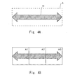
- a case of forming an arrow shape 91 in a stereolithography region A as shown in Fig. 4A is described hereinafter.
- the stereolithography region A is divided into projection regions A1, A2 and A3, which correspond to light exposure regions, as shown in Fig. 4B, and then exposure data is created for each of the projection regions.
- a stereolithography apparatus performs exposure in such a way that the projection regions are adjacent to each other with no space in between.
- such exposure allows the formation of a three-dimensional model in an integral form.
- flaking or cracking can occur at the boundaries between the projection regions or bumps and dips can be formed on an exposure surface or in the lamination direction, causing degradation of surface roughness and reduction of strength.
- the present invention has been accomplished to solve the above problems and an object of the present invention is thus to provide a stereolithography method capable of accurately forming a three-dimensional model with a desired shape.
- a stereolithography method that forms a cured resin layer by selectively applying light to liquid photocurable resin and laminates cured resin layers on one another to create a three-dimensional model, wherein the light is applied by repeating one-shot exposure in each projection region, and the projection region includes an overlap region at a boundary between adjacent projection regions.
- an area of the projection region is 100 mm 2 or smaller, it is possible to form a three-dimensional model more accurately.
- the stereolithography method according to the present invention is used where a thickness of one layer of the cured resin layers is 10 ⁇ m or smaller, it is possible to form a three-dimensional model more accurately. It is preferred that an exposure amount in the overlap region is adjusted to be equal to an exposure amount in a region different from the overlap region.
- an exposure amount in the overlap region in the first projection region decreases toward a center of the second projection region
- an exposure amount in the overlap region in the second projection region decreases toward a center of the first projection region
- an exposure amount in the overlap region in the first projection region is substantially half an exposure amount in a region different from the overlap region
- an exposure amount in the overlap region in the second projection region is substantially half an exposure amount in a region different from the overlap region. It is also preferred to stagger a position of the overlap region or alter a shape of the overlap region between adjacent cured resin layers.
- the stereolithography method according to the present invention is suitable for use where the liquid photocurable resin is cured by light reflected by a digital mirror device.
- the present invention can provide a stereolithography method capable of accurately forming a three-dimensional model with a desired shape.
- a stereolithography apparatus 100 includes a light source 1, a digital mirror device (DMD) 2, a lens 3, a stereolithography table 4, a dispenser 5, a recoater 6, a controller 7, and a storage unit 8.
- DMD digital mirror device
- a stereolithography apparatus 100 includes a light source 1, a digital mirror device (DMD) 2, a lens 3, a stereolithography table 4, a dispenser 5, a recoater 6, a controller 7, and a storage unit 8.
- the light source 1 emits a laser beam.
- the light source 1 may be a laser diode (LD) or a ultraviolet (UV) lamp that emits laser light with a wavelength of 405 nm, for example.
- the digital mirror device (DMD) 2 is a device that is developed by Texas Instruments, Inc., in which several hundreds of thousands to several millions of, e.g., 480 to 1310 thousands of, independently-driven micromirrors are arrayed on a CMOS semiconductor. Such micromirrors can be inclined at about ⁇ 10 degrees, e.g. ⁇ 12 degrees, around a diagonal line by the electrostatic field. Each microlens has a rectangular shape with one side of about 10 ⁇ m, e.g. 13.68 ⁇ m in length.
- the DMD 2 that is used in the first embodiment has a rectangular shape of 40.8 ⁇ 31.8 mm as a whole (a mirror part has a rectangular shape of 14.0 ⁇ 10.5 mm), and it is composed of 786,432 micromirrors, one side of each having a length of 13.68 ⁇ m.
- the DMD 2 reflects a laser beam that is emitted from the light source 1 by each micromirror, so that only the laser light that is reflected by a micromirror that is controlled at a given angle by the controller 7 is applied to the photocurable resin 9 on the stereolithography table 4 through the condenser lens 3.
- the lens 3 directs the laser beam that is reflected by the DMD 2 onto the photocurable resin 9 to form a projection region.
- the lens 3 may be a condenser lens using a convex lens, or a concave lens.
- the use of the concave lens allows formation of a projection region that is larger than an actual size of DSM.
- the lens 3 of the first embodiment is a condenser lens, which condenses the incident light at a magnification of about 15 times and focuses the light on the photocurable resin 9.
- the stereolithography table 4 is a flat support on which cured resins are sequentially deposited and placed.
- the stereolithography table 4 is horizontally and vertically movable by a driving mechanism, or a moving mechanism, which is not shown.
- the driving mechanism enables stereolithography over a desired range.
- the dispenser 5 contains a photocurable resin 10 and supplies a predetermined amount of the photocurable resin 10 to a prescribed position.
- the recoater 6 includes a blade mechanism and a moving mechanism, for example, and it evenly deposits the photocurable resin 10.
- the controller 7 controls the light source 1, the DMD 2, the stereolithography table 4, the dispenser 5 and the recoater 6 according to control data that includes exposure data.
- the controller 7 may be realized by installing a given program onto a computer.
- a typical computer configuration includes a central processing unit (CPU) and a memory.
- the CPU and the memory are connected to an external storage device, such as a hard disk device as an auxiliary storage device, through a bus.
- the external storage device serves as the storage unit 8 of the controller 7.
- a storage medium driving device such as a flexible disk device, a hard disk device, or a CD-ROM drive, is connected to the bus through a controller of each type.
- a portable storage medium, such as a flexible disk is inserted to the storage medium driving device such as a flexible disk device.
- the storage medium may store a given computer program that gives a command to a CPU or the like in cooperation with an operating system to implement the present embodiment.
- the storage unit 8 stores control data that includes exposure data of cross-sections that are obtained by slicing a three-dimensional model to be formed into a plurality of layers.
- the controller 7 mainly controls the angle of each micromirror in the DMD 2 and the movement of the stereolithography table 4 (i.e. the position of the laser beam exposure range on a three-dimensional model) based on the exposure data that is stored in the storage unit 8, thus executing the formation of a three-dimensional model.
- a computer program is executed by being loaded to a memory.
- the computer program may be stored in a storage medium by being compressed or divided into a plurality of pieces.
- a user interface hardware may be provided.
- the user interface hardware may be a pointing device for input such as a mouse, a keyboard, a display for presenting visual data to a user, or the like.
- the photocurable resin 10 may be a resin that is cured by visible light and light outside the visible light spectrum. For example, an acrylic resin with a cure depth of 15 ⁇ m or above (500 mJ/cm 2 ) and a viscosity of 1500 to 2500 Pa ⁇ s (25°C), which is responsive to a wavelength of 405 nm, may be used.
- Stereolithography operation of the stereolithography apparatus 100 is described hereinafter.
- the photocurable resin 10 in a non-cured state is poured into the dispenser 5.
- the stereolithography table 4 is located at an initial position.
- the dispenser 5 supplies a predetermined amount of the photocurable resin 10 onto the stereolithography table 4.
- the recoater 6 sweeps to spread the photocurable resin 10, thereby forming one coating layer to be cured.
- a laser beam that is emitted from the light source 1 is incident on the DMD 2.
- the DMD 2 is controlled by the controller 7 according to the exposure data that is stored in the storage unit 8 so as to adjust the angle of a micromirror that corresponds to a part of the photocurable resin 10 which is to be exposed to a laser beam.
- a laser beam that is reflected by the relevant micromirror is thereby applied to the photocurable resin 10 through the condenser lens 3, and laser beams that are reflected by other micromirrors are not applied to the photocurable resin 10.
- the application of a laser beam to the photocurable resin 10 may be performed for 0.4 seconds, for example.
- a projection region on the photocurable resin 10 is about 1.3 ⁇ 1.8 mm, for example, and it may be reduced to about 0.6 ⁇ 0.9 mm. In general, the area of the projection region is preferably 100 mm 2 or smaller. With the use of a concave lens as the lens 3, a projection region may be enlarged to about 6 ⁇ 9 cm.
- a projection region is enlarged to be larger than this size, the energy density of a laser beam that is applied to the projection region decreases, which can cause insufficient curing of the photocurable resin 10.
- a laser beam is applied one shot at a time in each projection region. The control of laser beam exposure to each projection region is described in detail later.
- the lamination pitch of one layer which is the thickness of a single cured resin layer, may be, for example, 1 to 50 ⁇ m, preferably 2 to 10 ⁇ m, and more preferably 5 to 10 ⁇ m.
- a second layer of a three-dimensional model with a desired shape is formed in the same process.
- the photocurable resin 10 that is supplied from the dispenser 5 is deposited with a uniform thickness on the outside of the cured resin layer which is formed as a first layer in such a way that it is spread to be larger than a three-dimensional model by the recoater 6.
- a laser beam is applied so as to form a second cured resin layer on top of the first cured resin layer.
- a third and subsequent cured resin layers are deposited sequentially in the same manner.
- a model that is formed on the stereolithography table 4 is taken out.
- the liquid photocurable resin that is attached to the surface of the model is removed by cleaning or the like, and, if necessary, the model may be further exposed to a UV lamp or the like or heated to thereby promote the curing.
- Fig. 2A is a top view showing the shape of a three-dimensional model to be formed.
- Fig. 2B is a view showing the positional relationship between a plurality of projection regions and a three-dimensional model.
- Fig. 2C is a graph showing the exposure amount at each position on X-X' in Fig. 2B.
- the dotted lines that extend downward in Fig. 2B are respectively connected with the dotted lines that extend upward in Fig. 2C.
- Fig. 2A a case of forming a three-dimensional model with an arrow shape when viewed from the top is described as shown in Fig. 2A.
- Fig. 2A a case of forming a three-dimensional model with an arrow shape when viewed from the top is described as shown in Fig. 2A.
- Fig. 2A is a case of forming a three-dimensional model with an arrow shape when viewed from the top.
- A indicates a stereolithography region that includes the three-dimensional model.
- the stereolithography region A is divided simply into projection regions which correspond to a laser beam applicable range.
- a projection region is 1/3 the size of the stereolithography region A in this example.
- the stereolithography method of the related art divides the stereolithography region A into three sections in such a way that projection regions do not overlap with each other, the present embodiment performs exposure on each of four projection regions.
- this embodiment performs exposure on four projection regions A1, A2, A3 and A4 as shown in Fig. 2B.
- the projection region A1 is an area of a light applicable range at the left end of the stereolithography region A.
- the projection region A2 is an area that is placed in such a way that its left end overlaps with the projection region A1.
- an overlap region B1 is formed at the boundary between the projection region A1 and the projection region A2.
- the projection region A3 is placed in such a way that its left end overlaps with the projection region A2.
- an overlap region B2 is formed at the boundary between the projection region A2 and the projection region A3.
- the projection region A4 is placed in such a way that its left end overlaps with the projection region A3.
- an overlap region B3 is formed at the boundary between the projection region A3 and the projection region A4.
- the width of the overlap regions B1, B2 and B3 may be several ⁇ m to several hundreds of ⁇ m, for example.
- the exposure data such that the exposure shape in each projection region is as illustrated in Fig. 2B. It is also necessary to create exposure data such that exposure position of a laser beam on a three-dimensional model moves so as to form the overlap regions B1, B2 and B3. It is thus needed to create the exposure data that causes a moving mechanism for moving a stereolithography table to move so as to form the overlap regions B1, B2 and B3. If a laser beam is applied onto a photocurable resin as illustrated in Fig. 2B, the exposure amount in the overlap regions B1, B2 and B3 is larger than that in the other regions. In this example, the exposure amount in the overlap regions B1, B2 and B3 is about twice as large as the exposure amount in the other regions.
- the stereolithography method according to the first embodiment performs exposure in such a way that there is an overlap region at the boundaries between the projection regions according to the exposure data that is created as described above. It is thereby possible to prevent the occurrence of flaking or cracking at the boundaries between the projection regions and the formation of bumps and dips on the exposure surface or in the lamination direction, thereby improving the surface roughness and strength and enabling the accurate formation of a three-dimensional model with a desired shape.
- the exposure amount in the overlap regions at the boundaries between the projection regions is larger than that in the other regions. Accordingly, the range of resin curing extends in the overlap regions, which can cause an excessive resin curing part. Such an excessive resin curing part is one factor of warpage deformation with time. Particularly, the adverse effect of the uneven exposure amount is significant in the microstereolithography where one-shot exposure area is 250 mm 2 or smaller.
- the second embodiment of the invention adjusts the exposure amount in the overlap regions (a total amount of overlap exposure) in such a way that it is equal to the exposure amount in the regions different from the overlap regions, which is, an exposure energy density.
- the exposure amount can be controlled in the same way as controlling the shading on a display screen, which is, by repetitively changing the angle of micromirrors in the DMD 2 at a certain frequency within one-time exposure period onto an exposure region to thereby adjust the exposure time of a laser beam from each micromirror.
- the present embodiment of the invention can control the exposure amount by the same control as when producing light and shade on a display screen in the DMD 2, it is possible to share the same data format, thus allowing the use of a bitmap format, which is a general screen display format, for example.
- Fig. 3A is the same view as Fig. 2B, and it is referred to for indicating the exposure positions in Figs. 3B and 3C.
- the dotted lines that extend downward in Fig. 3A are respectively connected with the dotted lines that extend upward in Fig. 3B.
- the exposure amount in the overlap region B1 in the projection region A1 gradually decreases toward the projection region A2.
- the exposure amount in the overlap region B1 in the projection region A1 decreases in direct proportion to the distance to the end of the projection region A1 on the side of the projection region A2.
- the exposure amount in the overlap region B1 in the projection region A2 gradually decreases toward the projection region A1.
- the exposure amount in the overlap region B1 in the projection region A2 decreases in direct proportion to the distance to the end of the projection region A2 on the side of the projection region A1. More specifically, because the exposure amount can be controlled by the same control as when producing shading on a display screen for each of regions that are exposed to a laser beam from each micromirror, the exposure amount in the overlap region B1 shown in Fig. 3B does not, to be exact, change in a continuous fashion relative to the exposure position but changes in a step-by-step fashion according to the number of micromirrors for the exposure position in the overlap region B1.
- the exposure amount in the overlap region B1 is basically a sum of the exposure amount in the projection region A1 and the exposure amount in the projection region A2.
- the exposure amount in the overlap region B1 is 1, which is the same as the exposure amount in the other regions.
- the exposure amount in the overlap region is not necessarily exactly the same as the exposure amount in the other regions, and it is preferred to adjust the exposure amount as appropriate according to a photocurable resin or a light source for exposure that are used.
- the exposure amount in the overlap regions B2 and B3 is also controlled to be 1, which is the same as the exposure amount in the other regions. Accordingly, the exposure amount in the laser beam exposure area, which includes the overlap regions B1, B2 and B3, is equal, thus remaining uniform. Therefore, the stereolithography method of the second embodiment prevents the occurrence of an excessive resin curing part and enables the accurate formation of a three-dimensional model with a desired shape. Particularly, if the exposure amount is adjusted as shown in Fig. 3B, a change in the exposure amount is gradual and there is no abrupt change in exposure amount. Thus, uneven curing is not likely to occur even if displacement occurs in a projection region. A decrease or increase in the exposure amount in the overlap regions may be represented by linear expression or by quadratic or higher order expression.
- the exposure amount may be adjusted as shown in Fig. 3C.
- the exposure amount in the overlap region B1 in the projection region A1 is controlled to be 0.5, which is half the amount in the other regions, and the exposure amount in the overlap region B1 in the projection region A2 is also controlled to 0.5.
- the exposure amount in the overlap region B1 which is basically a sum of the exposure amount in the projection region A1 and the exposure amount in the projection region A2, is 1, thus being the same as the exposure amount in the other regions.
- the exposure amount in the overlap regions B2 and B3 is also controlled to be 1, which is the same as the exposure amount in the other regions.
- the exposure amount in the part where a three-dimensional model exists which includes the overlap regions B1, B2 and B3, is equal, thus remaining uniform. It is thereby possible to prevent the occurrence of an excessive resin curing part and enable the accurate formation of a three-dimensional model with a desired shape in this case also.
- a stereolithography apparatus may be provided with a function for switching between a mode of forming an overlap region and a mode of not forming an overlap region.
- the projections regions are arranged in one row in the above embodiments, they may be arranged two dimensionally in a vertical and horizontal array, in which case also overlap regions may be formed at the boundaries between the adjacent projection regions. In such a case, the overlap regions are formed at four surrounding positions because there are adjacent projection regions in four directions on the upper, lower, left and right sides.
- a DMD is used as a device for modulating a light beam emitted from a light source in the above embodiments
- the present invention is not limited thereto, and a liquid crystal device capable of adjusting the amount of light passing therethrough for each of minute regions, which is pixels, may be used instead.
- the DMD is more preferable than the liquid crystal device in terms of contrast.
- only one layer is described in the above embodiments, it is preferred to form overlap regions in each of a plurality of layers that are used for forming a three-dimensional mode. The position of the overlap regions may be staggered in adjacent layers. Further, the shape of the overlap regions may be different between adjacent layers.
- the stereolithography method according to the present invention can be used in manufacture of microreactors, micromachine parts, micro-optical devices, microsensors, optical elements and so on.
Landscapes
- Engineering & Computer Science (AREA)
- Chemical & Material Sciences (AREA)
- Materials Engineering (AREA)
- Physics & Mathematics (AREA)
- Manufacturing & Machinery (AREA)
- Mechanical Engineering (AREA)
- Optics & Photonics (AREA)
- Health & Medical Sciences (AREA)
- Toxicology (AREA)
- Oral & Maxillofacial Surgery (AREA)
- Thermal Sciences (AREA)
Applications Claiming Priority (2)
| Application Number | Priority Date | Filing Date | Title |
|---|---|---|---|
| JP2005099800A JP4525424B2 (ja) | 2005-03-30 | 2005-03-30 | 光造形方法 |
| PCT/JP2006/305411 WO2006109425A1 (fr) | 2005-03-30 | 2006-03-17 | Procede de stereolithographie |
Publications (2)
| Publication Number | Publication Date |
|---|---|
| EP1864785A1 true EP1864785A1 (fr) | 2007-12-12 |
| EP1864785A4 EP1864785A4 (fr) | 2012-11-07 |
Family
ID=37086716
Family Applications (1)
| Application Number | Title | Priority Date | Filing Date |
|---|---|---|---|
| EP06729400A Withdrawn EP1864785A4 (fr) | 2005-03-30 | 2006-03-17 | Procede de stereolithographie |
Country Status (7)
| Country | Link |
|---|---|
| US (1) | US20090133800A1 (fr) |
| EP (1) | EP1864785A4 (fr) |
| JP (1) | JP4525424B2 (fr) |
| KR (1) | KR100895566B1 (fr) |
| CN (1) | CN101151141A (fr) |
| TW (1) | TW200642830A (fr) |
| WO (1) | WO2006109425A1 (fr) |
Cited By (27)
| Publication number | Priority date | Publication date | Assignee | Title |
|---|---|---|---|---|
| WO2008088642A3 (fr) * | 2007-01-17 | 2008-10-02 | 3D Systems Inc | Ensemble imageur et procédé d'imagerie solide |
| US7614866B2 (en) | 2007-01-17 | 2009-11-10 | 3D Systems, Inc. | Solid imaging apparatus and method |
| EP1946910A3 (fr) * | 2007-01-17 | 2010-02-24 | 3D Systems, Inc. | Assemblage d'imageur et procédé d'imagerie solide |
| US7758799B2 (en) | 2005-04-01 | 2010-07-20 | 3D Systems, Inc. | Edge smoothness with low resolution projected images for use in solid imaging |
| US7771183B2 (en) | 2007-01-17 | 2010-08-10 | 3D Systems, Inc. | Solid imaging system with removal of excess uncured build material |
| US8003039B2 (en) | 2007-01-17 | 2011-08-23 | 3D Systems, Inc. | Method for tilting solid image build platform for reducing air entrainment and for build release |
| US8105066B2 (en) | 2007-01-17 | 2012-01-31 | 3D Systems, Inc. | Cartridge for solid imaging apparatus and method |
| US8221671B2 (en) | 2007-01-17 | 2012-07-17 | 3D Systems, Inc. | Imager and method for consistent repeatable alignment in a solid imaging apparatus |
| US9034237B2 (en) | 2012-09-25 | 2015-05-19 | 3D Systems, Inc. | Solid imaging systems, components thereof, and methods of solid imaging |
| WO2015092016A1 (fr) * | 2013-12-20 | 2015-06-25 | Luxexcel Holding B.V. | Procédé pour imprimer une structure tridimensionnelle de guidage de la lumière par le durcissement de gouttelettes d'un matériau d'impression par irradiation de lumière |
| CN105690772A (zh) * | 2016-04-08 | 2016-06-22 | 中国工程物理研究院机械制造工艺研究所 | 用于微机械机构的免装配制造方法及装置 |
| WO2016116320A1 (fr) * | 2015-01-22 | 2016-07-28 | Way To Production Gmbh | Procédé d'exposition à l'action de la lumière d'une zone tridimensionnelle |
| EP3053729A1 (fr) * | 2015-02-04 | 2016-08-10 | Visitech As | Procédé d'exposition d'un matériau polymérisable photographique pour la solidification d'une couche de matériau par couche, afin de construire un objet 3D |
| US9415544B2 (en) | 2006-08-29 | 2016-08-16 | 3D Systems, Inc. | Wall smoothness, feature accuracy and resolution in projected images via exposure levels in solid imaging |
| NO20190617A1 (en) * | 2019-05-16 | 2020-11-17 | Visitech As | System and method for exposing a material with images |
| US11731367B2 (en) | 2021-06-23 | 2023-08-22 | General Electric Company | Drive system for additive manufacturing |
| US11813799B2 (en) | 2021-09-01 | 2023-11-14 | General Electric Company | Control systems and methods for additive manufacturing |
| US11826950B2 (en) | 2021-07-09 | 2023-11-28 | General Electric Company | Resin management system for additive manufacturing |
| US11951679B2 (en) | 2021-06-16 | 2024-04-09 | General Electric Company | Additive manufacturing system |
| US11958250B2 (en) | 2021-06-24 | 2024-04-16 | General Electric Company | Reclamation system for additive manufacturing |
| US11958249B2 (en) | 2021-06-24 | 2024-04-16 | General Electric Company | Reclamation system for additive manufacturing |
| US12296535B2 (en) | 2021-08-24 | 2025-05-13 | General Electric Company | Attachment structure for additive manufacturing |
| US12370741B2 (en) | 2021-08-13 | 2025-07-29 | General Electric Company | Material deposition assembly for additive manufacturing |
| US12403654B2 (en) | 2022-09-30 | 2025-09-02 | General Electric Company | Systems and methods for additive manufacturing |
| US12409604B2 (en) | 2022-03-23 | 2025-09-09 | General Electric Company | Systems and methods for additive manufacturing |
| US12434436B2 (en) | 2021-02-26 | 2025-10-07 | General Electric Company | Accumalator assembly for additive manufacturing |
| US12589549B2 (en) | 2021-04-27 | 2026-03-31 | General Electric Company | Systems and methods for additive manufacturing |
Families Citing this family (25)
| Publication number | Priority date | Publication date | Assignee | Title |
|---|---|---|---|---|
| JP5151098B2 (ja) * | 2006-03-31 | 2013-02-27 | Jsr株式会社 | 微小造形法用光硬化性液状樹脂組成物、これを用いた3次元構造体の製造方法、及び金属型 |
| JP4957242B2 (ja) * | 2006-12-28 | 2012-06-20 | ソニー株式会社 | 光造形装置 |
| JP5234315B2 (ja) * | 2007-12-03 | 2013-07-10 | ソニー株式会社 | 光造形装置および光造形方法 |
| CN101554778B (zh) * | 2008-04-11 | 2011-05-11 | 西安科技大学 | 面整体光固化快速成型方法及装置 |
| US8048359B2 (en) | 2008-10-20 | 2011-11-01 | 3D Systems, Inc. | Compensation of actinic radiation intensity profiles for three-dimensional modelers |
| US8691476B2 (en) | 2011-12-16 | 2014-04-08 | Taiwan Semiconductor Manufacturing Company, Ltd. | EUV mask and method for forming the same |
| CN102674241B (zh) * | 2012-05-31 | 2015-01-28 | 东南大学 | 一种基于无掩模灰度光刻的变高度微流道制作方法 |
| US9102098B2 (en) | 2012-12-05 | 2015-08-11 | Wobbleworks, Inc. | Hand-held three-dimensional drawing device |
| CN103465641B (zh) * | 2013-09-13 | 2015-09-16 | 绍兴迅实电子科技有限公司 | 一种面成型3d打印设备 |
| CN103448249B (zh) * | 2013-09-13 | 2016-06-15 | 张靖 | 一种面成型3d打印方法和系统 |
| CN104015363B (zh) * | 2014-06-20 | 2016-08-24 | 大族激光科技产业集团股份有限公司 | 一种大尺寸物件的dlp快速成型系统及方法 |
| JP6505517B2 (ja) * | 2015-06-18 | 2019-04-24 | ローランドディー.ジー.株式会社 | 三次元造形装置 |
| AT518101B1 (de) * | 2015-12-17 | 2018-05-15 | Stadlmann Klaus | Verfahren zum Erzeugen eines dreidimensionalen Gegenstands |
| JP2017177347A (ja) * | 2016-03-28 | 2017-10-05 | ローランドディー.ジー.株式会社 | 三次元造形装置および三次元造形物の造形方法 |
| JP2018108703A (ja) * | 2017-01-05 | 2018-07-12 | ローランドディー.ジー.株式会社 | 制御装置 |
| KR101966333B1 (ko) * | 2017-01-24 | 2019-04-08 | 주식회사 캐리마 | 복수개의 화면으로 분할되는 대형화면 노광시스템을 구비한 3d프린터 |
| US20180243989A1 (en) * | 2017-02-28 | 2018-08-30 | 3D Systems, Inc. | Three dimensional printing systems with overlapping light engines |
| JPWO2019116455A1 (ja) * | 2017-12-12 | 2020-12-24 | 株式会社ニコン | 造形システム及び造形方法 |
| JPWO2019116454A1 (ja) * | 2017-12-12 | 2020-12-24 | 株式会社ニコン | 処理装置、処理方法、マーキング方法、及び、造形方法 |
| JP2019162788A (ja) | 2018-03-19 | 2019-09-26 | 株式会社リコー | 液体吐出装置、液体吐出システム、液体吐出方法およびプログラム |
| CN111361147B (zh) * | 2020-05-27 | 2020-08-25 | 上海唯视锐光电技术有限公司 | 渐变拼接的多次曝光大画幅3d打印系统及使用方法 |
| US11707883B2 (en) | 2020-11-20 | 2023-07-25 | General Electric Company | Foil interaction device for additive manufacturing |
| USD995629S1 (en) | 2021-01-29 | 2023-08-15 | Wobble Works, Inc. | Drawing tool |
| JP7842863B2 (ja) | 2021-11-23 | 2026-04-08 | ウォブルワークス・インコーポレイテッド | ハンドヘルド3次元描画装置 |
| KR102870961B1 (ko) * | 2022-10-05 | 2025-10-21 | 오스템임플란트 주식회사 | 3d 프린팅을 위한 레이어 이미지 제공 방법, 그리고 이를 구현하기 위한 장치 |
Family Cites Families (12)
| Publication number | Priority date | Publication date | Assignee | Title |
|---|---|---|---|---|
| US5182056A (en) * | 1988-04-18 | 1993-01-26 | 3D Systems, Inc. | Stereolithography method and apparatus employing various penetration depths |
| US5965079A (en) * | 1995-04-25 | 1999-10-12 | 3D Systems, Inc. | Method and apparatus for making a three-dimensional object by stereolithography |
| JP3490491B2 (ja) * | 1994-02-24 | 2004-01-26 | 株式会社東芝 | 光造形品の製造方法及び光造形装置 |
| EP1077125A1 (fr) * | 1999-08-19 | 2001-02-21 | British Aerospace Public Limited Company | Article présentant des zones de densités différentes, et procédé stéréolithographique pour sa fabrication |
| JP4519274B2 (ja) * | 2000-06-06 | 2010-08-04 | ナブテスコ株式会社 | 光造形装置および光造形方法 |
| US6500378B1 (en) * | 2000-07-13 | 2002-12-31 | Eom Technologies, L.L.C. | Method and apparatus for creating three-dimensional objects by cross-sectional lithography |
| US20020149137A1 (en) * | 2001-04-12 | 2002-10-17 | Bor Zeng Jang | Layer manufacturing method and apparatus using full-area curing |
| JP2002331591A (ja) * | 2001-05-08 | 2002-11-19 | Fuji Photo Film Co Ltd | 光造形方法 |
| WO2003039844A1 (fr) * | 2001-10-30 | 2003-05-15 | Concept Laser Gmbh | Procede de production de pieces frittees tridimensionnelles |
| JP3792168B2 (ja) * | 2002-03-12 | 2006-07-05 | ナブテスコ株式会社 | 光学的立体造形方法および装置 |
| EP1666235B1 (fr) * | 2003-09-11 | 2012-11-07 | Nabtesco Corporation | Dispositifs de formation d'un objet optique tridimensionnel et procédés les utilisant |
| JP4459741B2 (ja) * | 2004-07-15 | 2010-04-28 | ナブテスコ株式会社 | 光学的立体造形方法 |
-
2005
- 2005-03-30 JP JP2005099800A patent/JP4525424B2/ja not_active Expired - Fee Related
-
2006
- 2006-03-17 CN CNA2006800105933A patent/CN101151141A/zh active Pending
- 2006-03-17 WO PCT/JP2006/305411 patent/WO2006109425A1/fr not_active Ceased
- 2006-03-17 US US11/909,816 patent/US20090133800A1/en not_active Abandoned
- 2006-03-17 KR KR1020077024922A patent/KR100895566B1/ko not_active Expired - Fee Related
- 2006-03-17 EP EP06729400A patent/EP1864785A4/fr not_active Withdrawn
- 2006-03-24 TW TW095110391A patent/TW200642830A/zh unknown
Cited By (39)
| Publication number | Priority date | Publication date | Assignee | Title |
|---|---|---|---|---|
| US7758799B2 (en) | 2005-04-01 | 2010-07-20 | 3D Systems, Inc. | Edge smoothness with low resolution projected images for use in solid imaging |
| US8703037B2 (en) | 2005-04-01 | 2014-04-22 | 3D Systems, Inc. | Edge smoothness with low resolution projected images for use in solid imaging |
| US9415544B2 (en) | 2006-08-29 | 2016-08-16 | 3D Systems, Inc. | Wall smoothness, feature accuracy and resolution in projected images via exposure levels in solid imaging |
| US8105066B2 (en) | 2007-01-17 | 2012-01-31 | 3D Systems, Inc. | Cartridge for solid imaging apparatus and method |
| US7731887B2 (en) | 2007-01-17 | 2010-06-08 | 3D Systems, Inc. | Method for removing excess uncured build material in solid imaging |
| US7706910B2 (en) | 2007-01-17 | 2010-04-27 | 3D Systems, Inc. | Imager assembly and method for solid imaging |
| US7771183B2 (en) | 2007-01-17 | 2010-08-10 | 3D Systems, Inc. | Solid imaging system with removal of excess uncured build material |
| US8003039B2 (en) | 2007-01-17 | 2011-08-23 | 3D Systems, Inc. | Method for tilting solid image build platform for reducing air entrainment and for build release |
| WO2008088642A3 (fr) * | 2007-01-17 | 2008-10-02 | 3D Systems Inc | Ensemble imageur et procédé d'imagerie solide |
| US8221671B2 (en) | 2007-01-17 | 2012-07-17 | 3D Systems, Inc. | Imager and method for consistent repeatable alignment in a solid imaging apparatus |
| US8465689B2 (en) | 2007-01-17 | 2013-06-18 | 3D Systems, Inc. | Elevator and method for tilting solid image build platform for reducing air entrainment and for build release |
| EP1946910A3 (fr) * | 2007-01-17 | 2010-02-24 | 3D Systems, Inc. | Assemblage d'imageur et procédé d'imagerie solide |
| US7614866B2 (en) | 2007-01-17 | 2009-11-10 | 3D Systems, Inc. | Solid imaging apparatus and method |
| US9034237B2 (en) | 2012-09-25 | 2015-05-19 | 3D Systems, Inc. | Solid imaging systems, components thereof, and methods of solid imaging |
| WO2015092016A1 (fr) * | 2013-12-20 | 2015-06-25 | Luxexcel Holding B.V. | Procédé pour imprimer une structure tridimensionnelle de guidage de la lumière par le durcissement de gouttelettes d'un matériau d'impression par irradiation de lumière |
| US10994474B2 (en) | 2013-12-20 | 2021-05-04 | Luxexcel Holding B.V. | Method for printing a three-dimensional light guiding structure by curing droplets of a printing material by light irradiation |
| AT516769A1 (de) * | 2015-01-22 | 2016-08-15 | Way To Production Gmbh | Verfahren zur Belichtung eines dreidimensionalen Bereichs |
| WO2016116320A1 (fr) * | 2015-01-22 | 2016-07-28 | Way To Production Gmbh | Procédé d'exposition à l'action de la lumière d'une zone tridimensionnelle |
| AT516769B1 (de) * | 2015-01-22 | 2017-12-15 | Way To Production Gmbh | Verfahren zur Belichtung eines dreidimensionalen Bereichs |
| WO2016124634A1 (fr) * | 2015-02-04 | 2016-08-11 | Visitech As | Procédé d'exposition d'un matériau photopolymérisable pour la solidification couche par couche de matériau afin de construire un objet en 3d |
| EP3053729A1 (fr) * | 2015-02-04 | 2016-08-10 | Visitech As | Procédé d'exposition d'un matériau polymérisable photographique pour la solidification d'une couche de matériau par couche, afin de construire un objet 3D |
| CN105690772B (zh) * | 2016-04-08 | 2017-10-31 | 中国工程物理研究院机械制造工艺研究所 | 用于微机械机构的免装配制造方法及装置 |
| CN105690772A (zh) * | 2016-04-08 | 2016-06-22 | 中国工程物理研究院机械制造工艺研究所 | 用于微机械机构的免装配制造方法及装置 |
| NO20190617A1 (en) * | 2019-05-16 | 2020-11-17 | Visitech As | System and method for exposing a material with images |
| US12434436B2 (en) | 2021-02-26 | 2025-10-07 | General Electric Company | Accumalator assembly for additive manufacturing |
| US12589549B2 (en) | 2021-04-27 | 2026-03-31 | General Electric Company | Systems and methods for additive manufacturing |
| US11951679B2 (en) | 2021-06-16 | 2024-04-09 | General Electric Company | Additive manufacturing system |
| US11731367B2 (en) | 2021-06-23 | 2023-08-22 | General Electric Company | Drive system for additive manufacturing |
| US11958250B2 (en) | 2021-06-24 | 2024-04-16 | General Electric Company | Reclamation system for additive manufacturing |
| US11958249B2 (en) | 2021-06-24 | 2024-04-16 | General Electric Company | Reclamation system for additive manufacturing |
| US12447682B2 (en) | 2021-06-24 | 2025-10-21 | General Electric Company | Reclamation system for additive manufacturing |
| US12521942B2 (en) | 2021-06-24 | 2026-01-13 | General Electric Company | Reclamation system for additive manufacturing |
| US11826950B2 (en) | 2021-07-09 | 2023-11-28 | General Electric Company | Resin management system for additive manufacturing |
| US12390986B2 (en) | 2021-07-09 | 2025-08-19 | General Electric Company | Resin management system for additive manufacturing |
| US12370741B2 (en) | 2021-08-13 | 2025-07-29 | General Electric Company | Material deposition assembly for additive manufacturing |
| US12296535B2 (en) | 2021-08-24 | 2025-05-13 | General Electric Company | Attachment structure for additive manufacturing |
| US11813799B2 (en) | 2021-09-01 | 2023-11-14 | General Electric Company | Control systems and methods for additive manufacturing |
| US12409604B2 (en) | 2022-03-23 | 2025-09-09 | General Electric Company | Systems and methods for additive manufacturing |
| US12403654B2 (en) | 2022-09-30 | 2025-09-02 | General Electric Company | Systems and methods for additive manufacturing |
Also Published As
| Publication number | Publication date |
|---|---|
| WO2006109425A1 (fr) | 2006-10-19 |
| TW200642830A (en) | 2006-12-16 |
| EP1864785A4 (fr) | 2012-11-07 |
| JP2006272916A (ja) | 2006-10-12 |
| CN101151141A (zh) | 2008-03-26 |
| US20090133800A1 (en) | 2009-05-28 |
| KR100895566B1 (ko) | 2009-04-29 |
| KR20080003379A (ko) | 2008-01-07 |
| JP4525424B2 (ja) | 2010-08-18 |
Similar Documents
| Publication | Publication Date | Title |
|---|---|---|
| US20090133800A1 (en) | Stereolithography method | |
| JP4950183B2 (ja) | ラピッドプロトタイピング装置およびラピッドプロトタイピングの方法 | |
| JPH0639928A (ja) | ステレオリソグラフ装置および使用方法 | |
| JP5133841B2 (ja) | スライス画像生成方法および造形装置 | |
| JP2007298990A (ja) | マスク露光により三次元物体を作製する装置及び方法 | |
| CN115257026A (zh) | 用于铸造聚合物产品的方法和装置 | |
| JP2002331591A (ja) | 光造形方法 | |
| JP2009132127A (ja) | 光造形装置および光造形方法 | |
| CN118003625A (zh) | 用于超高吞吐量增材制造的系统、方法及材料 | |
| US11919235B2 (en) | Techniques for generation and direction of light in additive fabrication and related systems and methods | |
| JP2017159557A (ja) | 三次元造形装置、造形物の製造方法、プログラム及び記録媒体 | |
| US7736577B2 (en) | Stereolithography apparatus and stereolithography method | |
| Xu et al. | Vibration-assisted vat photopolymerization for pixelated-aliasing-free surface fabrication | |
| KR102763206B1 (ko) | 마스크리스 리소그래피를 위한 다중 톤 방식 | |
| JP2008238652A (ja) | 光造形方法及び光造形装置 | |
| JP2022023065A (ja) | インプリントリソグラフィプロセスにおける光学層の構成 | |
| JP4049654B2 (ja) | 3次元造形装置および3次元造形方法 | |
| JP2006272917A (ja) | 光造形方法 | |
| JP5151319B2 (ja) | 光造形方法 | |
| JP4626446B2 (ja) | 光造形装置および光造形方法 | |
| JP7650157B2 (ja) | はみ出し制御のための枠硬化分解能を改善する方法および装置 | |
| CN109982830B (zh) | 信息处理设备、成形装置、信息处理方法和程序 | |
| JP4650161B2 (ja) | 光造形装置および光造形方法 | |
| JP2008238651A (ja) | 光造形方法 | |
| US20150248062A1 (en) | Digital exposure method and digital exposure apparatus for performing the same |
Legal Events
| Date | Code | Title | Description |
|---|---|---|---|
| PUAI | Public reference made under article 153(3) epc to a published international application that has entered the european phase |
Free format text: ORIGINAL CODE: 0009012 |
|
| 17P | Request for examination filed |
Effective date: 20070918 |
|
| AK | Designated contracting states |
Kind code of ref document: A1 Designated state(s): CH DE FR LI |
|
| RBV | Designated contracting states (corrected) |
Designated state(s): CH DE FR LI |
|
| DAX | Request for extension of the european patent (deleted) | ||
| A4 | Supplementary search report drawn up and despatched |
Effective date: 20121009 |
|
| RIC1 | Information provided on ipc code assigned before grant |
Ipc: B29C 67/00 20060101AFI20121002BHEP |
|
| STAA | Information on the status of an ep patent application or granted ep patent |
Free format text: STATUS: THE APPLICATION IS DEEMED TO BE WITHDRAWN |
|
| 18D | Application deemed to be withdrawn |
Effective date: 20130507 |