EP1865485A2 - Appareil d'affichage à plasma et circuit de balayage a surtension reduite - Google Patents
Appareil d'affichage à plasma et circuit de balayage a surtension reduite Download PDFInfo
- Publication number
- EP1865485A2 EP1865485A2 EP07252020A EP07252020A EP1865485A2 EP 1865485 A2 EP1865485 A2 EP 1865485A2 EP 07252020 A EP07252020 A EP 07252020A EP 07252020 A EP07252020 A EP 07252020A EP 1865485 A2 EP1865485 A2 EP 1865485A2
- Authority
- EP
- European Patent Office
- Prior art keywords
- electrodes
- scan
- voltage
- power supply
- condenser
- Prior art date
- Legal status (The legal status is an assumption and is not a legal conclusion. Google has not performed a legal analysis and makes no representation as to the accuracy of the status listed.)
- Withdrawn
Links
- 230000000694 effects Effects 0.000 title description 4
- 239000000919 ceramic Substances 0.000 claims abstract description 37
- 239000003792 electrolyte Substances 0.000 claims description 22
- 239000000758 substrate Substances 0.000 claims description 19
- 230000004044 response Effects 0.000 claims description 5
- 230000006378 damage Effects 0.000 description 3
- 239000011521 glass Substances 0.000 description 3
- 238000010586 diagram Methods 0.000 description 2
- 230000009467 reduction Effects 0.000 description 2
- 230000008859 change Effects 0.000 description 1
- 238000001914 filtration Methods 0.000 description 1
- 238000003780 insertion Methods 0.000 description 1
- 230000037431 insertion Effects 0.000 description 1
- 230000010354 integration Effects 0.000 description 1
- 230000004048 modification Effects 0.000 description 1
- 238000012986 modification Methods 0.000 description 1
- 238000005192 partition Methods 0.000 description 1
- 239000000126 substance Substances 0.000 description 1
Images


Classifications
-
- G—PHYSICS
- G09—EDUCATION; CRYPTOGRAPHY; DISPLAY; ADVERTISING; SEALS
- G09G—ARRANGEMENTS OR CIRCUITS FOR CONTROL OF INDICATING DEVICES USING STATIC MEANS TO PRESENT VARIABLE INFORMATION
- G09G3/00—Control arrangements or circuits, of interest only in connection with visual indicators other than cathode-ray tubes
- G09G3/20—Control arrangements or circuits, of interest only in connection with visual indicators other than cathode-ray tubes for presentation of an assembly of a number of characters, e.g. a page, by composing the assembly by combination of individual elements arranged in a matrix no fixed position being assigned to or needed to be assigned to the individual characters or partial characters
- G09G3/22—Control arrangements or circuits, of interest only in connection with visual indicators other than cathode-ray tubes for presentation of an assembly of a number of characters, e.g. a page, by composing the assembly by combination of individual elements arranged in a matrix no fixed position being assigned to or needed to be assigned to the individual characters or partial characters using controlled light sources
- G09G3/28—Control arrangements or circuits, of interest only in connection with visual indicators other than cathode-ray tubes for presentation of an assembly of a number of characters, e.g. a page, by composing the assembly by combination of individual elements arranged in a matrix no fixed position being assigned to or needed to be assigned to the individual characters or partial characters using controlled light sources using luminous gas-discharge panels, e.g. plasma panels
- G09G3/288—Control arrangements or circuits, of interest only in connection with visual indicators other than cathode-ray tubes for presentation of an assembly of a number of characters, e.g. a page, by composing the assembly by combination of individual elements arranged in a matrix no fixed position being assigned to or needed to be assigned to the individual characters or partial characters using controlled light sources using luminous gas-discharge panels, e.g. plasma panels using AC panels
- G09G3/296—Driving circuits for producing the waveforms applied to the driving electrodes
-
- H—ELECTRICITY
- H03—ELECTRONIC CIRCUITRY
- H03K—PULSE TECHNIQUE
- H03K19/00—Logic circuits, i.e. having at least two inputs acting on one output; Inverting circuits
-
- G—PHYSICS
- G09—EDUCATION; CRYPTOGRAPHY; DISPLAY; ADVERTISING; SEALS
- G09G—ARRANGEMENTS OR CIRCUITS FOR CONTROL OF INDICATING DEVICES USING STATIC MEANS TO PRESENT VARIABLE INFORMATION
- G09G2330/00—Aspects of power supply; Aspects of display protection and defect management
- G09G2330/02—Details of power systems and of start or stop of display operation
- G09G2330/025—Reduction of instantaneous peaks of current
Definitions
- the present invention generally relates to an image display apparatus and a display apparatus drive circuit, and particularly relates to a plasma display apparatus and a plasma display panel drive circuit.
- a plasma display panel has two glass substrates which have electrodes formed thereon and define a space therebetween that is filled with discharge gas, and generates electric discharge by applying voltages between the electrodes so as to induce light emission from fluorescent substance provided on the substrates in response to the ultraviolet light generated by the electric discharge, thereby displaying an image.
- Plasma display panels are widely used as large-screen display apparatuses due to the facts that it is easy to make a large-sized screen, that its self-light- emission nature ensures high display quality, and that the response speed is high.
- X electrodes and Y electrodes extending in parallel are formed, and address electrodes are provided to run perpendicularly to the X and Y electrodes.
- the X and Y electrodes serve to generate sustain discharges for display-purpose light emission.
- the sustain discharges are generated by applying voltage pulses repeatedly between the X electrodes and the Y electrode.
- the Y electrodes also serve as scan electrodes for use in the writing of display data.
- the address electrodes serve to select discharge cells that emit light, and apply address-voltage pulses responsive to display data in order to generate write discharge for selecting discharge cells between the Y electrodes and the address electrodes.
- an X-electrode drive circuit for driving the X electrodes does is to supply the voltage for generating sustain discharge, so that the X-electrode drive circuit is implemented as a simple switch circuit comprised of MOSFETs.
- a Y-electrode drive circuit for driving the Y electrodes not only supplies the voltage for generating sustain discharge, but also serves to scan the Y electrodes at the time of writing display data. The Y-electrode drive circuit is thus implemented by using scan ICs usable for the scanning purpose.
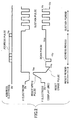
- FIG. 1 is a drawing showing an example of the configuration of a related-art Y-electrode drive circuit.
- a Y-electrode drive circuit of Fig. 1 includes switches 11 through 19, a power supply 20, diodes 21 through 23, resistors 24 and 25, and condensers 26 through 29.
- Each switch shown in Fig. 1 is implemented by use of one or more MOSFETs. The ON/OFF control of each switch is performed by controlling a signal voltage applied to the gate node of the one or more MOSFETs.
- a scan IC (scan integrated circuit) 10 includes the switch 11, the switch 12, the diode 21, and the diode 22.
- An output signal line OUT extending from the scan IC 10 is connected to a corresponding one of the Y electrodes.
- a plurality of sets each comprised of the switch 11, the switch 12, the diode 21, the diode 22, and the output signal line OUT are provided in a single scan IC 10, so that each scan IC 10 is capable of scanning a plurality of Y electrodes (e.g., 192 Y electrodes).
- the power supply 20 supplies a direct-current voltage VSC that is equal to Vs + V2.
- the electrolyte condenser 26 absorbs voltage fluctuation, so that the power supply voltage VDH of the scan IC 10 is maintained at the constant voltage VSC relative to GND.
- GND is the ground-potential side of the scan IC 10. As will be described in the following, however, GND is not fixed to a ground potential, but is caused to vary in accordance with its expected operation.
- the voltage VSC is a high voltage higher than approximately 50V.
- Fig. 2 is a drawing showing an example of waveforms for driving X electrodes, Y electrodes, and address electrodes.
- the drive period of a plasma display panel mainly consists of a reset period, an address period, and a sustain period.
- each display pixel is initialized.
- the address period that follows, pixels to be displayed (i.e., pixels to emit light) is selected.
- the sustain period that comes last, the selected pixels are caused to emit light.
- the switch 15 and the switch 13 are turned on, so that the voltage V1 + Vs is supplied to the scan IC 10 via the switch 13.
- the received voltage V1 + Vs is supplied to the Y electrode of the panel via the diode 22 connected in parallel to the switch 12.
- the voltage V1 + Vs is applied to all the Y electrodes provided in the panel.
- An electric current then flows from the panel to the ground via the switch 12, the switch 19, and the switch 18, thereby forming a reset erase pulse having a gentle slope reaching -Vs as shown in Fig. 2.
- scan voltage pulses at the -Vy level are successively applied to the Y electrodes serving as scan electrodes, thereby driving the Y electrodes one by one.
- address voltage pulses at the Va level are applied to the address electrodes. This serves to select display cells on each scan line.
- the GND side of the scan IC 10 is fixed to -Vy (-(V2 + Vs)) in the circuit shown in Fig. 1, and either one of the switch 11 and the switch 12 is turned on to scan and drive the corresponding Y electrode.
- the switch 11 and the switch 12 are turned off and on, respectively, thereby outputting a -Vy pulse to the output signal line OUT.
- the switch 11 and the switch 12 are turned on and off, respectively, thereby keeping the output signal line OUT at VDH of the scan IC 10.
- the switching operations of the switch 11 and switch 12 of the scan IC 10 control the application of a pulse to the Y electrode as described above, thereby making it possible to perform the driving of individual Y electrodes independently of each other.
- sustain pulses stain voltage pulses
- Vs common Vs level
- VDH of the scan IC 10 is set to about 120 V above GND in a stable state, but may increase to approximately 150 V due to the serge voltage described above.
- the maximum tolerable voltage of the scan IC 10 is about 170 V. In some cases, VDS increases to a voltage close to such maximum tolerable voltage.
- IC components may have their usable life shortened or suffer an increased failure rate if they are used in the condition where a voltage close to the maximum tolerable voltage (i.e., the limit voltage above which circuit destruction occurs) is applied. That is, they become more likely to fail when used in a stressful condition. If IC components are used in a low stress condition with an applied voltage much lower than the maximum tolerable voltage, on the other hand, they can be used for a long time with a low failure rate. Such reduction of stress is called derating. In order to provide sufficient derating to secure sufficient reliability with respect to circuit components in the scan IC 10, there is a need to address the serge voltage.
- a voltage close tolerable voltage i.e., the limit voltage above which circuit destruction occurs
- Reliability is conventionally ensured by using a high-tolerance-level scan IC 10 or by inserting a large film condenser close to the scan IC 10 for the purpose of eliminating a serge voltage.
- a high-tolerance-level scan IC 10 is expensive.
- the use of such scan ICs 10 leads to a price increase of plasma display panels.
- the use of a large film condenser also leads to a cost increase, and also results in an increase in circuit size.
- Patent Document 1 Japanese Patent Application Publication No. 6-186927
- the invention aims to provide a plasma display apparatus and a plasma display panel drive circuit in which the effect of serge voltage is reduced without increasing cost and circuit size.
- the invention provides a plasma display apparatus which includes an IC that operates with a power supply voltage, of which a difference between a ground potential and a power supply potential is substantially more than 50 V, a ceramic condenser disposed in a vicinity of the IC and coupled between the ground potential and the power supply potential of the IC, and a resistor connected in series with the ceramic condenser between the ground potential and the power supply potential.
- a drive circuit for successively scanning and driving first electrodes while third electrodes are driven in a display panel in which display cells are constituted at least by a set of electrodes including the first electrodes extending in a first direction, second electrodes extending in the first direction, and the third electrodes extending in a second direction substantially perpendicular to the first direction, includes an IC configured to successively scan and drive the first electrodes by operating with a power supply voltage, of which a difference between a ground potential and a power supply potential is substantially more than 50 V, a ceramic condenser disposed in a vicinity of the IC and coupled between the ground potential and the power supply potential of the IC, and a resistor connected in series with the ceramic condenser between the ground potential and the power supply potential.
- a filter circuit comprised of the series connection of the ceramic condenser and the resistor is provided in a close proximity of the scan IC between VDH and GND to suppress a serge voltage, thereby making it possible to ensure the use of the scan IC in a low-stress-level condition at a voltage sufficiently lower than the maximum tolerable voltage.
- FIG. 3 is a block diagram showing a main part of a plasma display apparatus to which the present invention is applied.
- a plasma display apparatus shown in Fig. 3 includes a display panel 31, an address driver circuit 32, a Y-electrode drive circuit 33, and an X-electrode drive circuit 34.
- the Y-electrode drive circuit 33 includes a scan driver circuit 41, a sustain pulse circuit 42, and a reset/address-voltage generating circuit 43.
- the X-electrode drive circuit 34 includes a sustain pulse circuit 45 and a reset/address-voltage generating circuit 46.
- Each circuit shown in Fig. 3 is controlled by various control signals such as a clock signal, display data, a vertical synchronizing signal, and a horizontal synchronizing signal.
- the address driver circuit 32 applies address-voltage pulses responsive to the display data to address electrodes A1 through Am in synchronization with the clock signal.
- the Y-electrode drive circuit 33 drives Y electrodes Y1 through Yn independently of each other.
- the X-electrode drive circuit 34 drives X electrodes X1 through Xn all together.
- Waveforms for driving the address electrodes, Y electrodes, and X electrodes through the operations of the address driver circuit 32, the Y-electrode drive circuit 33, and the X-electrode drive circuit 34 are the same as those used in the related-art configuration as shown in Fig. 2, for example.
- each display pixel is initialized.
- pixels to be displayed i.e., pixels to emit light
- the sustain period that comes last the selected pixels are caused to emit light.
- the reset/address-voltage generating circuit 43 of the Y-electrode drive circuit 33 In the reset period, the reset/address-voltage generating circuit 43 of the Y-electrode drive circuit 33 generates a reset voltage, so that the scan driver circuit 41 applies the reset voltage to all the Y electrodes Y1 through Yn. Further, a reset voltage generated by the reset/address-voltage generating circuit 46 of the X-electrode drive circuit 34 is applied to all the X electrodes X1 through Xn.
- the scan driver circuit 41 drives the Y electrodes Y1 through Yn successively one by one based on the address voltage generated by the reset/address-voltage generating circuit 43, and, in conjunction therewith, the address driver circuit 32 applies address-voltage pulses for one horizontal line responsive to the display data to the address electrodes A1 through Am. Cells to be displayed are selected in this manner, thereby controlling the display/non-display (selection/non-selection) of each display cell (pixel) 48.
- sustain voltage pulses generated by sustain pulse circuit 42 are applied to the Y electrodes Y1 through Yn via the scan driver circuit 41, and sustain voltage pulses generated by the sustain pulse circuit 45 are applied to the X electrodes X1 through Xn from the X-electrode drive circuit 34.
- the application of these sustain voltage pulses generates sustain discharge between an X electrode and a Y electrode at the cells selected as display cells.
- the address electrodes A1 through Am, X electrodes X1 through Xn, and Y electrodes Y1 through Yn are disposed between a front glass substrate and a rear glass substrate of the display panel 31. Further, partition walls are provided between the address electrodes A1 through Am.
- the number of light emissions of each display cell may be controlled to achieve the displaying of gray-scale tones.
- Electric discharge in the plasma display apparatus can assume only one of the two states, i.e., either the ON-state or the OFF-state, so that the number of light emissions is controlled to represent the level of brightness, i.e., gray-scale tones.
- one frame is divided into a plurality of sub-fields (e.g., 10 sub-fields).
- Each sub-field is constituted by a reset period, an address period, and a sustain period, and the length of the sustain period, i.e., the number of light emissions, is made to vary from sub-field to sub-field.
- the ratio of the lengths of the sustain periods from the first sub-field to the tenth sub-field may be set to 1:2:4:8: ... :512.
- One or more sub-fields are selected and subjected to discharge in response to the gray-scale level of a cell to be displayed, thereby displaying the cell at the desired gray-scale level.
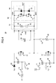
- Fig. 4 is a drawing showing an example of the configuration of the Y-electrode drive circuit 33 according to the present invention.
- the same elements as those of Fig. 1 are referred to by the same numerals, and a description thereof will be omitted.
- the Y-electrode drive circuit 33 of Fig. 4 includes a chip ceramic condenser 52 and a chip resistor 53 in addition to switches 11 through 19, a power supply 20, diodes 21 through 23, resistors 24 and 25, and condensers 26 through 29, which are the same as those shown in Fig. 1.
- the chip ceramic condenser 52 and the chip resistor 53 together constitute a filter circuit 51 for the purpose of suppressing a serge voltage.
- a scan IC 10 includes the switch 11, the switch 12, the diode 21, and the diode 22.
- An output signal line OUT extending from the scan IC 10 is connected to a corresponding one of the Y electrodes.
- a plurality of sets each comprised of the switch 11, the switch 12, the diode 21, the diode 22, and the output signal line OUT are provided in a single scan IC 10, so that each scan IC 10 is capable of scanning a plurality of Y electrodes (e.g., 192 Y electrodes).
- the portion of the Y-electrode drive circuit 33 that is not implemented on a scan-drive-module substrate 50 is shared by all the Y electrodes.
- the scan IC 10 is implemented on the scan-drive-module substrate 50 (printed circuit board). Only one scan IC 10 is shown with respect to one scan-drive-module substrate 50 for the sake of convenience of illustration. In reality, however, a plurality of scan ICs 10 (see Fig. 6) are mounted on one scan-drive-module substrate 50.
- the reset period the reset voltage is supplied to the scan ICs 10, and is applied to all the Y electrodes Y1 through Yn via paths provided in the scan ICs 10.
- the switching operations of the switch 11 and switch 12 of the scan IC 10 control the application of a pulse to the Y electrode, thereby making it possible to perform the driving of individual Y electrodes independently of each other to apply a scan pulse to a successively selected one of the Y electrodes.
- the sustain voltage is supplied to the scan ICs 10, and is applied to all the Y electrodes Y1 through Yn via paths provided in the scan ICs 10.
- the Y-electrode drive circuit 33 of Fig. 4 includes the chip ceramic condenser 52 and the chip resistor 53 situated in a close vicinity of the scan IC 10 on the scan-drive-module substrate 50, and are inserted between VDH and GND of the scan IC 10.
- the filtering effect of the filter circuit 51 comprised of the chip ceramic condenser 52 and the chip resistor 53 prevents VDH from reaching a high voltage level significantly exceeding its stable-state voltage level due to the superimposition of a serge voltage appearing on the output signal line OUT.
- the integration effect of the chip ceramic condenser 52 serves to smooth a steep waveform of the serge voltage, thereby suppressing an increase in VDH.
- the chip resistor 53 connected in series with the chip ceramic condenser 52 between VDH and GND is thus designed to have such a resistance that the resistor is destroyed in response to an excessive electric current responsive to such an excessive voltage. Namely, provision is made such that the chip resistor 53 is destroyed to result in an open-path state before the chip ceramic condenser 52 is destroyed to result in a short-circuit state. With this provision, the scan IC 10 is prevented from becoming incapable of operation by avoiding short-circuiting between VDH and GND even if an excessively large serge voltage is applied.
- a series connection of a ceramic condenser and a resistance is used to provide a configuration that provides an open-path state upon destruction, thereby making it viable to use a ceramic condenser.
- a ceramic condenser as used in the present invention is inexpensive compared with a film condenser that was conventionally used, thereby helping to achieve cost reduction.
- the chip ceramic condenser 52 used in the present invention is a ceramic condenser having a chip shape with a laminated structure, and may have a size of 2 mm by 1.25 mm, for example. The use of the chip ceramic condenser 52 thus helps to reduce the circuit size. Further, with chip shape, a stress applied to the condenser is small at the time of mounding on a substrate, thereby lowering the possibility of the component being damaged.
- the present invention uses the filter circuit 51 comprised of a series connection of the chip ceramic condenser 52 and the chip resistor 53 that is positioned in a close proximity of the scan IC 10 between VDH and GND to suppress a serge voltage, thereby making it possible to ensure the use of the scan IC 10 in a low-stress-level condition at a voltage sufficiently lower than the maximum tolerable voltage.
- This achieves a circuit configuration ensuring sufficient derating and high reliability with respect to the scan IC 10 by using a low-cost, small-size circuit.
- Figs. 5A and 5B are drawings showing examples of voltage waveforms actually observed between VDH and GND.
- Fig. 5A illustrates the way a voltage between VDH and GND changes during a sustain period in the related-art Y-electrode drive circuit (Fig. 1).
- Fig. 5B illustrates the way a voltage between VDH and GND changes during a sustain period in the Y-electrode drive circuit (Fig. 4) according to the present invention.
- a serge voltage is superimposed so that a voltage reaching 148.4 V at its peak is generated.
- the filter circuit 51 comprised of the chip ceramic condenser 52 and the chip resistor 53 suppresses a serge voltage, so that the maximum peak voltage is only 127.2 V.
- Fig. 6 is a drawing for explaining a variation of the Y-electrode drive circuit 33 of the present invention. What is shown in Fig. 6 is a configuration of the Y-electrode drive circuit 33 as actually implemented on circuit boards. Among the portions constituting the Y-electrode drive circuit 33 shown in Fig. 4, the portions other than the scan IC 10 and the filter circuit 51 implemented on the scan-drive-module substrate 50 are shown as a drive circuit 60.
- various voltages and voltage pulses generated by the drive circuit 60 for the reset purpose, address-scan purpose, and sustain- discharge purpose are supplied to a plurality of scan ICs 10 implemented on scan-drive-module substrates 50 via board connectors 61.
- Two scan-drive-module substrates 50 are connected to one drive circuit 60, and four scan ICs 10 are mounted on each scan-drive-module substrate 50.
- the number of Y electrodes driven by each scan IC 10 is 192, so that a total of 1536 Y electrodes are driven.
- the output signal lines of the scan ICs 10 are connected to the Y electrodes Y1 through Yn of the display panel 31 via flexible cables 62.
- One electrolyte condenser 26 as shown in Fig. 4 is provided in the drive circuit 60.
- the power supply 20 charges the electrolyte condenser 26 provided in the drive circuit 60 with the voltage VSC, and the charged voltage is supplied to each scan IC 10 from the electrolyte condenser 26.
- Each of such supply paths extends from the electrolyte condenser 26 and passes through the drive circuit 60 and one of the board connectors 61 to reach a scan IC 10 through an interconnect provided on the scan-drive-module substrate 50.
- a serge voltage appearing as superimposed on VDH of the scan IC 10 differs depending on the distance between the electrolyte condenser 26 and a scan IC 10, i.e., depending on the length of the above-described supply path.
- the serge voltage is relatively small in a scan IC 10 that is positioned at a short distance from the electrolyte condenser (voltage supply source) 26, i.e., in a scan IC 10 that has a short supply path.
- the serge voltage is relatively large in a scan IC 10 that is positioned at a long distance from the electrolyte condenser (voltage supply source) 26, i.e., in a scan IC 10 that has a long supply path.
- IC4, IC5, IC6, and IC7 among the 8 scan ICs 10 are positioned at relatively short distances from the electrolyte condenser 26, so that the serge voltage is relatively small.
- IC1, IC2, IC3, and IC8, for example, are positioned at a relatively long distance from the electrolyte condenser 26, so that the serge voltage is relatively large.
- the filter circuit 51 of the present invention is provided only with respect to IC1, IC2, IC3, and IC8, i.e., with respect to the scan ICs 10 that are positioned at long distances from the electrolyte condenser 26 and suffer relatively large serge voltages.
- the filter circuit 51 may be provided only with respect to some scan ICs 10 that are positioned at relatively long distances from the electrolyte condenser 26 among all the scan ICs 10. This can further reduce the cost and circuit size compared with a case in which the filter circuit 51 is provided in all the scan ICs 10. If a serge voltage is not ignorable in the scan ICs 10 (e.g., IC4, IC5, IC6, and IC7 in the example shown in Fig.
- the filter circuit 51 may be provided in all the scan ICs 10 (i.e., IC1, IC2, IC3, IC4, IC5, IC6, IC7, and IC8).
- the filter circuit is provided in a scan IC of the Y-electrode drive circuit
- the present invention is not limited to its application to a scan IC of the Y-electrode drive circuit.
- the filter circuit of the present invention can be utilized regardless of the type of the IC to suppress the serge voltage.
Landscapes
- Engineering & Computer Science (AREA)
- Physics & Mathematics (AREA)
- Computer Hardware Design (AREA)
- Power Engineering (AREA)
- Plasma & Fusion (AREA)
- General Physics & Mathematics (AREA)
- Theoretical Computer Science (AREA)
- Computing Systems (AREA)
- General Engineering & Computer Science (AREA)
- Mathematical Physics (AREA)
- Control Of Indicators Other Than Cathode Ray Tubes (AREA)
- Control Of Gas Discharge Display Tubes (AREA)
Applications Claiming Priority (1)
| Application Number | Priority Date | Filing Date | Title |
|---|---|---|---|
| JP2006159943A JP2007328179A (ja) | 2006-06-08 | 2006-06-08 | プラズマディスプレイ装置及びプラズマディスプレイパネルの駆動回路 |
Publications (1)
| Publication Number | Publication Date |
|---|---|
| EP1865485A2 true EP1865485A2 (fr) | 2007-12-12 |
Family
ID=38229546
Family Applications (1)
| Application Number | Title | Priority Date | Filing Date |
|---|---|---|---|
| EP07252020A Withdrawn EP1865485A2 (fr) | 2006-06-08 | 2007-05-17 | Appareil d'affichage à plasma et circuit de balayage a surtension reduite |
Country Status (5)
| Country | Link |
|---|---|
| US (1) | US20070285353A1 (fr) |
| EP (1) | EP1865485A2 (fr) |
| JP (1) | JP2007328179A (fr) |
| KR (1) | KR100833927B1 (fr) |
| CN (1) | CN101086814A (fr) |
Families Citing this family (2)
| Publication number | Priority date | Publication date | Assignee | Title |
|---|---|---|---|---|
| JP2008281706A (ja) * | 2007-05-09 | 2008-11-20 | Hitachi Ltd | プラズマディスプレイ装置 |
| CN102592556A (zh) * | 2012-02-22 | 2012-07-18 | 鞍山亚世光电显示有限公司 | 一种低功耗电子价签显示模块 |
Family Cites Families (10)
| Publication number | Priority date | Publication date | Assignee | Title |
|---|---|---|---|---|
| JP2000250425A (ja) * | 1999-02-25 | 2000-09-14 | Fujitsu Ltd | ドライバic実装モジュール |
| SG115510A1 (en) * | 2001-12-20 | 2005-10-28 | Nitto Denko Corp | Cover tape for the electronic part conveyance, process for its production and electronic part conveying member |
| KR100448191B1 (ko) * | 2002-02-19 | 2004-09-10 | 삼성전자주식회사 | 플라즈마 디스플레이장치의 무효전력회수장치와무효전력회수방법 |
| KR100573127B1 (ko) * | 2003-11-25 | 2006-04-24 | 삼성에스디아이 주식회사 | 에너지 재생 회로를 포함하는 플라즈마 디스플레이 패널의구동장치 |
| KR20050080696A (ko) * | 2004-02-10 | 2005-08-17 | 엘지전자 주식회사 | 플라즈마 디스플레이 패널의 구동장치 |
| KR100546091B1 (ko) * | 2004-05-21 | 2006-01-26 | 엘지전자 주식회사 | 플라즈마 표시 패널의 구동 장치 |
| KR100571200B1 (ko) * | 2004-06-04 | 2006-04-17 | 엘지전자 주식회사 | 플라즈마 디스플레이 패널 구동장치 |
| US7030595B2 (en) * | 2004-08-04 | 2006-04-18 | Nanopower Solutions Co., Ltd. | Voltage regulator having an inverse adaptive controller |
| JP5084134B2 (ja) * | 2005-11-21 | 2012-11-28 | 日本電気株式会社 | 表示装置及びこれらを用いた機器 |
| KR100708862B1 (ko) * | 2005-12-30 | 2007-04-17 | 삼성에스디아이 주식회사 | 플라즈마 표시 장치 및 그 구동 장치 |
-
2006
- 2006-06-08 JP JP2006159943A patent/JP2007328179A/ja active Pending
-
2007
- 2007-02-08 US US11/703,841 patent/US20070285353A1/en not_active Abandoned
- 2007-02-15 KR KR1020070015768A patent/KR100833927B1/ko not_active Expired - Fee Related
- 2007-02-16 CN CNA2007100788344A patent/CN101086814A/zh active Pending
- 2007-05-17 EP EP07252020A patent/EP1865485A2/fr not_active Withdrawn
Also Published As
| Publication number | Publication date |
|---|---|
| US20070285353A1 (en) | 2007-12-13 |
| KR20070117442A (ko) | 2007-12-12 |
| JP2007328179A (ja) | 2007-12-20 |
| KR100833927B1 (ko) | 2008-05-30 |
| CN101086814A (zh) | 2007-12-12 |
Similar Documents
| Publication | Publication Date | Title |
|---|---|---|
| JP4162434B2 (ja) | プラズマディスプレイパネルの駆動方法 | |
| KR100641371B1 (ko) | 플라즈마 디스플레이 패널 장치 | |
| US20010026254A1 (en) | Driving method for plasma display panel | |
| US20070057870A1 (en) | Plasma display device and method of driving the same | |
| US6727659B2 (en) | Apparatus and method for driving plasma display panels | |
| KR100499375B1 (ko) | 플라즈마 디스플레이 패널의 구동장치 및 방법 | |
| KR100490633B1 (ko) | 플라즈마 디스플레이 패널 및 이의 구동 방법 | |
| EP1865485A2 (fr) | Appareil d'affichage à plasma et circuit de balayage a surtension reduite | |
| JP2005309397A (ja) | プラズマディスプレイパネル、プラズマディスプレイ装置及びプラズマディスプレイパネルの駆動方法 | |
| US20030057855A1 (en) | Method and device to drive a plasma display | |
| CN100412925C (zh) | 等离子显示装置及其驱动方法 | |
| KR100627412B1 (ko) | 플라즈마 표시 장치 및 그 구동 방법 | |
| US7642995B2 (en) | Plasma display panel driving device and method | |
| KR20050110946A (ko) | 플라즈마 디스플레이 패널과 그의 구동방법 | |
| US20080024395A1 (en) | Plasma display apparatus | |
| JP5086639B2 (ja) | プラズマディスプレイパネルの駆動装置 | |
| JP2006146215A (ja) | プラズマ表示装置及びその駆動方法 | |
| CN1937017A (zh) | 等离子体显示面板驱动 | |
| US20060125727A1 (en) | Plasma display apparatus and driving method thereof | |
| KR100728782B1 (ko) | 플라즈마 표시 장치 및 그 구동 방법 | |
| KR100707467B1 (ko) | 플라즈마 디스플레이 장치 | |
| JP2005338119A (ja) | プラズマディスプレイ装置 | |
| EP1775700A2 (fr) | Dispositif d'affichage à plasma et procédé de pilotage correspondant | |
| EP1622115A2 (fr) | Appareil d'affichage à plasma et méthode de commande d'un tel appareil | |
| US20050219155A1 (en) | Driving method of display panel |
Legal Events
| Date | Code | Title | Description |
|---|---|---|---|
| PUAI | Public reference made under article 153(3) epc to a published international application that has entered the european phase |
Free format text: ORIGINAL CODE: 0009012 |
|
| 17P | Request for examination filed |
Effective date: 20070606 |
|
| AK | Designated contracting states |
Kind code of ref document: A2 Designated state(s): AT BE BG CH CY CZ DE DK EE ES FI FR GB GR HU IE IS IT LI LT LU LV MC MT NL PL PT RO SE SI SK TR |
|
| AX | Request for extension of the european patent |
Extension state: AL BA HR MK YU |
|
| RAP1 | Party data changed (applicant data changed or rights of an application transferred) |
Owner name: HITACHI PLASMA DISPLAY LIMITED |
|
| STAA | Information on the status of an ep patent application or granted ep patent |
Free format text: STATUS: THE APPLICATION HAS BEEN WITHDRAWN |
|
| 18W | Application withdrawn |
Effective date: 20090203 |