EP1865486A2 - Affichage électroluminescent organique et son procédé de commande - Google Patents
Affichage électroluminescent organique et son procédé de commande Download PDFInfo
- Publication number
- EP1865486A2 EP1865486A2 EP07251605A EP07251605A EP1865486A2 EP 1865486 A2 EP1865486 A2 EP 1865486A2 EP 07251605 A EP07251605 A EP 07251605A EP 07251605 A EP07251605 A EP 07251605A EP 1865486 A2 EP1865486 A2 EP 1865486A2
- Authority
- EP
- European Patent Office
- Prior art keywords
- organic electroluminescence
- emission control
- subframes
- signal
- scan
- Prior art date
- Legal status (The legal status is an assumption and is not a legal conclusion. Google has not performed a legal analysis and makes no representation as to the accuracy of the status listed.)
- Ceased
Links
Images

Classifications
-
- G—PHYSICS
- G09—EDUCATION; CRYPTOGRAPHY; DISPLAY; ADVERTISING; SEALS
- G09G—ARRANGEMENTS OR CIRCUITS FOR CONTROL OF INDICATING DEVICES USING STATIC MEANS TO PRESENT VARIABLE INFORMATION
- G09G3/00—Control arrangements or circuits, of interest only in connection with visual indicators other than cathode-ray tubes
- G09G3/20—Control arrangements or circuits, of interest only in connection with visual indicators other than cathode-ray tubes for presentation of an assembly of a number of characters, e.g. a page, by composing the assembly by combination of individual elements arranged in a matrix no fixed position being assigned to or needed to be assigned to the individual characters or partial characters
- G09G3/22—Control arrangements or circuits, of interest only in connection with visual indicators other than cathode-ray tubes for presentation of an assembly of a number of characters, e.g. a page, by composing the assembly by combination of individual elements arranged in a matrix no fixed position being assigned to or needed to be assigned to the individual characters or partial characters using controlled light sources
- G09G3/30—Control arrangements or circuits, of interest only in connection with visual indicators other than cathode-ray tubes for presentation of an assembly of a number of characters, e.g. a page, by composing the assembly by combination of individual elements arranged in a matrix no fixed position being assigned to or needed to be assigned to the individual characters or partial characters using controlled light sources using electroluminescent panels
- G09G3/32—Control arrangements or circuits, of interest only in connection with visual indicators other than cathode-ray tubes for presentation of an assembly of a number of characters, e.g. a page, by composing the assembly by combination of individual elements arranged in a matrix no fixed position being assigned to or needed to be assigned to the individual characters or partial characters using controlled light sources using electroluminescent panels semiconductive, e.g. using light-emitting diodes [LED]
- G09G3/3208—Control arrangements or circuits, of interest only in connection with visual indicators other than cathode-ray tubes for presentation of an assembly of a number of characters, e.g. a page, by composing the assembly by combination of individual elements arranged in a matrix no fixed position being assigned to or needed to be assigned to the individual characters or partial characters using controlled light sources using electroluminescent panels semiconductive, e.g. using light-emitting diodes [LED] organic, e.g. using organic light-emitting diodes [OLED]
- G09G3/3225—Control arrangements or circuits, of interest only in connection with visual indicators other than cathode-ray tubes for presentation of an assembly of a number of characters, e.g. a page, by composing the assembly by combination of individual elements arranged in a matrix no fixed position being assigned to or needed to be assigned to the individual characters or partial characters using controlled light sources using electroluminescent panels semiconductive, e.g. using light-emitting diodes [LED] organic, e.g. using organic light-emitting diodes [OLED] using an active matrix
- G09G3/3258—Control arrangements or circuits, of interest only in connection with visual indicators other than cathode-ray tubes for presentation of an assembly of a number of characters, e.g. a page, by composing the assembly by combination of individual elements arranged in a matrix no fixed position being assigned to or needed to be assigned to the individual characters or partial characters using controlled light sources using electroluminescent panels semiconductive, e.g. using light-emitting diodes [LED] organic, e.g. using organic light-emitting diodes [OLED] using an active matrix with pixel circuitry controlling the voltage across the light-emitting element
-
- G—PHYSICS
- G09—EDUCATION; CRYPTOGRAPHY; DISPLAY; ADVERTISING; SEALS
- G09G—ARRANGEMENTS OR CIRCUITS FOR CONTROL OF INDICATING DEVICES USING STATIC MEANS TO PRESENT VARIABLE INFORMATION
- G09G3/00—Control arrangements or circuits, of interest only in connection with visual indicators other than cathode-ray tubes
- G09G3/20—Control arrangements or circuits, of interest only in connection with visual indicators other than cathode-ray tubes for presentation of an assembly of a number of characters, e.g. a page, by composing the assembly by combination of individual elements arranged in a matrix no fixed position being assigned to or needed to be assigned to the individual characters or partial characters
- G09G3/22—Control arrangements or circuits, of interest only in connection with visual indicators other than cathode-ray tubes for presentation of an assembly of a number of characters, e.g. a page, by composing the assembly by combination of individual elements arranged in a matrix no fixed position being assigned to or needed to be assigned to the individual characters or partial characters using controlled light sources
- G09G3/30—Control arrangements or circuits, of interest only in connection with visual indicators other than cathode-ray tubes for presentation of an assembly of a number of characters, e.g. a page, by composing the assembly by combination of individual elements arranged in a matrix no fixed position being assigned to or needed to be assigned to the individual characters or partial characters using controlled light sources using electroluminescent panels
-
- G—PHYSICS
- G09—EDUCATION; CRYPTOGRAPHY; DISPLAY; ADVERTISING; SEALS
- G09G—ARRANGEMENTS OR CIRCUITS FOR CONTROL OF INDICATING DEVICES USING STATIC MEANS TO PRESENT VARIABLE INFORMATION
- G09G3/00—Control arrangements or circuits, of interest only in connection with visual indicators other than cathode-ray tubes
- G09G3/20—Control arrangements or circuits, of interest only in connection with visual indicators other than cathode-ray tubes for presentation of an assembly of a number of characters, e.g. a page, by composing the assembly by combination of individual elements arranged in a matrix no fixed position being assigned to or needed to be assigned to the individual characters or partial characters
- G09G3/2007—Display of intermediate tones
-
- G—PHYSICS
- G09—EDUCATION; CRYPTOGRAPHY; DISPLAY; ADVERTISING; SEALS
- G09G—ARRANGEMENTS OR CIRCUITS FOR CONTROL OF INDICATING DEVICES USING STATIC MEANS TO PRESENT VARIABLE INFORMATION
- G09G3/00—Control arrangements or circuits, of interest only in connection with visual indicators other than cathode-ray tubes
- G09G3/20—Control arrangements or circuits, of interest only in connection with visual indicators other than cathode-ray tubes for presentation of an assembly of a number of characters, e.g. a page, by composing the assembly by combination of individual elements arranged in a matrix no fixed position being assigned to or needed to be assigned to the individual characters or partial characters
- G09G3/2007—Display of intermediate tones
- G09G3/2018—Display of intermediate tones by time modulation using two or more time intervals
- G09G3/2022—Display of intermediate tones by time modulation using two or more time intervals using sub-frames
- G09G3/2025—Display of intermediate tones by time modulation using two or more time intervals using sub-frames the sub-frames having all the same time duration
-
- G—PHYSICS
- G09—EDUCATION; CRYPTOGRAPHY; DISPLAY; ADVERTISING; SEALS
- G09G—ARRANGEMENTS OR CIRCUITS FOR CONTROL OF INDICATING DEVICES USING STATIC MEANS TO PRESENT VARIABLE INFORMATION
- G09G2300/00—Aspects of the constitution of display devices
- G09G2300/08—Active matrix structure, i.e. with use of active elements, inclusive of non-linear two terminal elements, in the pixels together with light emitting or modulating elements
- G09G2300/0809—Several active elements per pixel in active matrix panels
- G09G2300/0842—Several active elements per pixel in active matrix panels forming a memory circuit, e.g. a dynamic memory with one capacitor
-
- G—PHYSICS
- G09—EDUCATION; CRYPTOGRAPHY; DISPLAY; ADVERTISING; SEALS
- G09G—ARRANGEMENTS OR CIRCUITS FOR CONTROL OF INDICATING DEVICES USING STATIC MEANS TO PRESENT VARIABLE INFORMATION
- G09G2300/00—Aspects of the constitution of display devices
- G09G2300/08—Active matrix structure, i.e. with use of active elements, inclusive of non-linear two terminal elements, in the pixels together with light emitting or modulating elements
- G09G2300/0809—Several active elements per pixel in active matrix panels
- G09G2300/0842—Several active elements per pixel in active matrix panels forming a memory circuit, e.g. a dynamic memory with one capacitor
- G09G2300/0861—Several active elements per pixel in active matrix panels forming a memory circuit, e.g. a dynamic memory with one capacitor with additional control of the display period without amending the charge stored in a pixel memory, e.g. by means of additional select electrodes
-
- G—PHYSICS
- G09—EDUCATION; CRYPTOGRAPHY; DISPLAY; ADVERTISING; SEALS
- G09G—ARRANGEMENTS OR CIRCUITS FOR CONTROL OF INDICATING DEVICES USING STATIC MEANS TO PRESENT VARIABLE INFORMATION
- G09G2320/00—Control of display operating conditions
- G09G2320/02—Improving the quality of display appearance
- G09G2320/0233—Improving the luminance or brightness uniformity across the screen
Definitions
- aspects of the present invention relate to an organic electroluminescence display and a driving method thereof. Particularly, but not exclusively the present invention relates to an organic electroluminescence display capable of displaying a grey level using a frequency characteristic of an organic electroluminescence device, and a driving method thereof.
- Flat panel displays contain a plurality of pixels in a matrix arrangement on a substrate and have the pixels set as a display area.
- scan lines and data lines are connected to pixels to display an image by selectively applying data signals to the pixels.
- Flat panel displays are classified into different type displays according to the driving mode of a pixel. These include passive matrix-type light-emitting displays and an active matrix-type light-emitting displays.
- An active matrix-type light-emitting display which emits light from every pixel has been used mainly due to better resolution, contrast, and operating speed.
- Active matrix-type light-emitting displays are used as displays for devices such as a personal computer, a portable phone, PDA, etc., or as monitors of various information appliances even though various other types of flat panel displays are known in the art.
- Other types of flat panel displays include liquid crystal displays (LCDs) using a liquid crystal panel, organic electroluminescence displays using an organic electroluminescence device, and plasma display panels (PDPs) using a plasma panel, etc.
- LCDs liquid crystal displays
- organic electroluminescence displays using an organic electroluminescence device
- PDPs plasma display panels
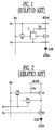
- FIG. 1 is a view of a circuit showing a pixel used in one related art organic electroluminescence display.
- the pixel is formed on a region where a data line (Dm) and a scan line (Sn) intersect, and includes a first transistor (T11), a second transistor (T21), a capacitor (Cst), a compensation circuit 11, and an organic electroluminescence device (OLED).
- the pixel is selected by receiving a scan signal through the scan line (Sn), and a data signal is transmitted to the selected pixel through the data line (Dm) so that a luminance corresponding to the data signal is displayed.
- each pixel is operated by receiving power from a first power supply (ELVdd) and a second power supply (ELVss).
- the first transistor (T11) allows a current to flow from a source to a drain according to a signal applied to a gate electrode, and has the gate electrode connected to the compensation circuit 11, the source connected to the first power supply (ELVdd), and the drain connected to the organic electroluminescence device (OLED).
- the second transistor (T21) transmits a data signal to the compensation circuit 11 according to the scan signal, and has a gate connected to the scan line (Sn), a source connected to the data line (Dm), and a drain connected to the compensation circuit 11.
- the capacitor (Cst) applies a voltage to the compensation circuit 11 that corresponds to the data signal.
- the capacitor (Cst) maintains a voltage of the data signal during a predetermined period. Therefore, the first transistor (T11) allows a current that corresponds to the voltage of the data signal to flow during a predetermined period.
- the second transistor since the first electrode of the capacitor is connected to the first power supply (ELVdd) and the second electrode is connected to the compensation circuit 11, the second electrode maintains a voltage that corresponds to the data signal. Accordingly, the voltage that corresponds to the data signal is maintained on the gate of the first transistor (T11) during the predetermined period.
- the compensation circuit 11 compensates for a threshold voltage of the first transistor (T11) by receiving a compensation control signal. Accordingly, the compensation circuit 11 prevents unevenness of a luminance due to unevenness of a threshold voltage.
- the compensation control signal may be transmitted by an additional signal line or may be transmitted by the scan line.
- the organic electroluminescence device has an organic film formed between an anode electrode and a cathode electrode so that the organic film is allowed to emit light. Light is emitted from the organic film if a current flows from the anode electrode to the cathode electrode.
- the anode electrode is connected to the drain of the first transistor (T11) and the cathode electrode is connected to the second power supply (ELVss).
- the organic film includes an emitting layer (EML), an electron transport layer (ETL) and a hole transport layer (HTL).
- the organic electroluminescence device may further include an electron injection layer (EIL) and a hole injection layer (HIL).
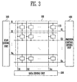
- FIG. 2 is a view of a circuit showing another pixel used in a related art organic electroluminescence display.
- the pixel includes a first transistor (T12), a second transistor (T22), a third transistor (T32), a fourth transistor (T42), a capacitor (Cst), and an organic electroluminescence device (OLED).
- the OLED shown is referred to as a current-driving pixel circuit for controlling a luminance using a current.
- the current-driving pixel circuit when the second transistor (T22) and the third transistor (T32) are in an ON state based on the scan signal, a current is generated in the first transistor (T12) that corresponds to a current flowing to the data line. At this time, a voltage corresponding to a capacity of the current is stored in the capacitor (Cst). Thereafter, when the second transistor (T22) and the third transistor (T32) are in an OFF state, the first transistor (T12) allows a current to flow to the organic electroluminescence device (OLED) due to the voltage stored in the capacitor (Cst).
- the current-driving pixel circuit as configured above does not have problems arising from an unevenness of a threshold voltage, etc., since the circuit uses the flowing current.
- the pixel as shown in FIG. 1 suffers from the drawback that it requires a circuit for compensating for an uneven threshold voltage, while the pixel as shown in FIG. 2 is not suitable for a large screen of an organic electroluminescence display since time needed for charging by a current is increased due to a parasitic capacitor, etc., and since the driving circuit is more complicated.
- an organic electroluminescence display has simple configurations of a pixel circuit and a driving circuit by using a frequency characteristic of an organic electroluminescence device to display a grey level, and a driving method thereof.
- a first aspect of the present invention provides an organic electroluminescence display as set out in claim 1. Preferred features are set out in claims 2 to 7.
- a second aspect of the present invention provides a method of driving an organic electroluminescence display as set out in claim 8, preferred features are set out in claims 9 to 11.
- a third aspect of the present invention provides a pixel of an electroluminescence device as set out in claim 12. Preferred features are set out in claims 13 and 14.
- FIG. 3 is a schematic view showing a configuration of an organic electroluminescence display according to a first embodiment of the present invention.
- the organic electroluminescence display includes a pixel unit 100, a data driving unit 200, a scan driving unit 300, and an emission control driving unit 400.
- the pixel unit 100 includes a plurality of data lines (D1, D2...Dm-1, Dm) and a plurality of scan lines (S1, S2...Sn-1, Sn), and a plurality of pixels formed in a region defined by the plurality of the data lines (D1, D2...Dm-1, Dm) and the plurality of the scan lines (S1, S2...Sn-1, Sn).
- the pixel 110 includes a pixel circuit and an organic electroluminescence device (not shown), and generates a pixel current in the pixel circuit to flow to the organic electroluminescence device.
- the pixel current flows in the pixels 110 according to data signals transmitted through the plurality of the data lines (D1, D2...Dm-1, Dm) and scan signals transmitted through the plurality of the scan lines (S1, S2...Sn-1, Sn).
- each pixel 110 distinguishes a plurality of subframes of the one frame.
- a grey level displayed in the pixel 110 is determined by a sum of luminances emitted during each period of the subframes.
- the data driving unit 200 is connected with the plurality of the data line (D1, D2...Dm-1, Dm), and generates n-bit data signals to be sequentially transmitted to the plurality of the data lines (D1, D2...Dm-1, Dm).
- the scan driving unit 300 is connected to the plurality of the scan lines (S1, S2...Sn-1, Sn), and generates scan signals to be transmitted to the plurality of the scan lines (S1, S2...Sn-1, Sn). Accordingly, the scan signals are transmitted according to each unit of the subframes, and then each row of the pixel unit 100 is sequentially selected so that the digital data signals are transmitted into the selected rows of the plurality of the scan lines (S1, S2...Sn-1, Sn).
- the emission control driving unit 400 transmits emission control signals to emission control lines (E1, E2,...En).
- the emission control signals have different frequencies in each subframe. Therefore, a brightness of the pixel 110 is determined by the emission control signals when the current generated by the data signal is transmitted to the organic electroluminescence device (OLED) according to the frequencies of the emission control signals.
- the scan driving unit 300 and the emission control driving unit 400 are shown as separate units, but it will be appreciated that separate units is not required. In other embodiments of the invention, the scan driving unit 300 and the emission control driving unit 400 may be combined.
- FIG. 4 is a diagram showing a change of luminances (brightness) relative to frequencies of an organic electroluminescence device used in the organic electroluminescence display as shown in FIG. 3.
- the luminance of the organic electroluminescence device diminishes when a high frequency signal is transmitted to the organic electroluminescence device, but the luminance of the organic electroluminescence device increases when a low frequency signal is inputted and passed through the organic electroluminescence device.
- the organic electroluminescence device (OLED) exhibits a high luminance if the inputted signal frequency is low, while the organic electroluminescence device (OLED) exhibits a low luminance if the inputted signal frequency is high.
- FIG. 5 is a view of a circuit showing an embodiment of the pixel used in the organic electroluminescence display as shown in FIG. 3.
- the pixel includes a first transistor (M11), a second transistor (M21), a third transistor (M31), a capacitor (Cst), and an organic electroluminescence device (OLED).
- the first to third transistors (M11 to M31) are implemented using a p-type metal-oxide semiconductor (PMOS) transistor. It will be understood that other types of transistors are usable.
- PMOS p-type metal-oxide semiconductor
- the first transistor (M11) has a gate connected to the first node (N 1), a source connected to the first power supply (ELUdd), and a drain connected to a source of the third transistor (M31). Accordingly, a current flows from the source to the drain of the first transistor (M31) according to the voltage transmitted to the first node (N1).
- the second transistor (M21) has a gate connected to the scan line (Sn), a source connected to the data line (Dm), and a drain connected to the first node (N1). Accordingly, the data signal flowing through the data line (Dm) is transmitted to the first node (N1) according to the scan signal transmitted through the scan line (Sn).
- the third transistor (M31) has a gate connected to the emission control line (En), a source connected to the drain of the first transistor (M11), and a drain connected to the organic electroluminescence device (OLED). Accordingly, a current flowing from the source to the drain of the third transistor (M31) is transmitted to the organic electroluminescence device (OLED) according to the emission control signal transmitted through the emission control line (En). Also, the emission control signal transmitted through the emission control line (En) has a frequency.
- the emission control signal repeats signals "0" and “1” to transmit the signals "0" and “1” to the gate of the third transistor (M31) if the digital data signal that is transmitted to the capacitor (Cst) is set to "0" (i.e., when the second transistor is in an OFF state).
- the third transistor (M31) carries out an ON/OFF operation according to the frequency of the respective emission control signal, and controls a frequency of the current transmitted to (or controls how frequently the current is transmitted to) the organic electroluminescence device (OLED).
- the digital data signal that is transmitted to the capacitor (Cst) is set to "1"
- the first transistor (M11) is in an OFF state and interrupts the current that is to flow to the organic electroluminescence device (OLED).
- the capacitor (Cst) has a first electrode connected to the first power supply (ELVdd) and a second electrode connected to the first node (N1) to maintain a voltage of the first node (N1) during a predetermined period. Accordingly, the voltage of the data signal is maintained at the first node (N1) by the capacitor (Cst) even when the second transistor (M21) is in an OFF state.
- the organic electroluminescence device receives the current whose frequency is controlled by the third transistor (M31) so that light is emitted and a grey level corresponding to the frequency is displayed.
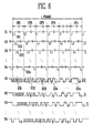
- FIG. 6 is a waveform diagram showing a method of driving the pixel as shown in FIG. 4.
- one frame is divided into n number of subframes (SF1, SF2, SF3....SFn) to correspond to an n-bit digital signal.
- the n number of the subframes (SF1, SF2, SF3....SFn) are operated to display a grey level in the organic electroluminescence device.
- the n number of the subframes (SF1, SF2, SF3....SFn) have the grey levels corresponding to the different brightnesses, based on the emission control signals (ES1, ES2...ESn-1,ESn).
- the ratio of the grey levels corresponding to the brightnesses of the first to n th subframes are 2 0 : 2 1 : 2 2 : 2 3 : 2 4 .... 2 n .
- the second transistors (M21) connected to each of the scan lines (S1, S2...Sn-1, Sn) are sequentially turned on.
- the emission control signal (ES 1) is transmitted to a gate of the third transistor (M31) through the emission control line (En) so as to be synchronized with the low state of the scan signals.
- each capacitor (Cst) stores a voltage difference of a voltage of the first-bit digital signal and a voltage of the first power supply (ELVdd).
- the second transistor (M21) connected to the scan lines (S1, S2...Sn-1, Sn) will be turned OFF.
- the first-bit digital data signal is stored in each capacitor (Cst)
- the first-bit digital data signal is continuously transmitted to the gate electrode of the first transistor (M11), and a current will continuously flow from a source to a drain of the first transistor (M11).
- the third transistor (M31) carries out a switching operation using the emission control signal (ES1), and the current, which flows from the source to the drain of the first transistor (M11), will be transmitted to the OLED according to a frequency of the emission control signal (ES1).
- the organic electroluminescence device has a characteristic as shown in FIG. 4, wherein the brightness diminishes if the current is supplied with a high frequency, while the brightness increases if the current is supplied with a low frequency and is passed through the organic electroluminescence device (OLED). Accordingly, the organic electroluminescence device (OLED) emits light according to the frequency of the emission control signal (ES1) corresponding to the first-bit digital data signal during a first subframe (SF1) period.
- ES1 emission control signal
- the organic electroluminescence device is not allowed to emit light if the digital data signal of the first bit is set to "1" (i.e., if turned OFF), and is allowed to emit light with a brightness corresponding to "2 0 " grey level if the digital data signal of the first bit is set to "0" (i.e., turned ON).
- each capacitor (Cst) stores a voltage difference of a voltage of the second-bit digital signal and a voltage of the first power supply (ELVdd).
- the second transistor (M21) will be turned OFF.
- the second-bit digital data signal is stored in each capacitor (Cst)
- the second-bit digital data signal is continuously transmitted to the gate electrode of the first transistor (M11), and a current will continuously flow from a source to a drain of the first transistor (M11).
- the third transistor (M31) carries out a switching operation using the emission control signal (ES2), and the current, which flows from the source to the drain of the first transistor (M11), will be transmitted to the OLED according to a frequency of the emission control signal (ES2).
- the organic electroluminescence device has a characteristic as shown in FIG. 4, wherein the brightness diminishes if the current is supplied with a high frequency, while the brightness decreases if the current is supplied with a low frequency, and is passed through the organic electroluminescence device (OLED). Accordingly, the organic electroluminescence device (OLED) emits light according to the frequency of the emission control signal (ES2) corresponding to the second-bit digital data signal during a second subframe period (SF2). That is, the organic electroluminescence device (OLED) is not allowed to emit the light if the digital data signal of the first bit is set to "1," and is allowed to emit the light with a brightness corresponding to "2 1 " grey level if it is set to "0.”
- ES2 emission control signal
- a current corresponding to the third-bit data signal will be transmitted to the OLED according to a frequency of the emission control signal (ES3), and therefore, the organic electroluminescence device (OLED) will emit light with a brightness corresponding to any one of "0" or “2 2 " grey levels during a third subframe period in the third subframe (SF3) of the one frame, as described above.
- ES3 emission control signal
- OLED organic electroluminescence device
- the same operation is carried out in each of the fourth subframe (SF4) to the n th subframe (SFn) of the one frame, and the current generated by the first transistor (M11) will be transmitted to the OLED according to a frequency of the emission control signals (ES4...ESn), and therefore, the organic electroluminescence device (OLED) will emit light with a brightness corresponding to "0" or "2 3 " to "2 n " grey levels.
- OLED organic electroluminescence device
- the organic electroluminescence display according to an embodiment of the present invention and the driving method thereof display a desired grey level achieved by the sum of the brightnesses of each of the subframes by utilizing a frequency characteristic of the organic electroluminescence device as shown in FIG. 4.
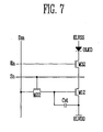
- FIG. 7 is a view of a circuit showing another embodiment of the pixel used in the organic electroluminescence display as shown in FIG. 3.
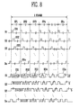
- FIG. 8 is a waveform view showing a method of driving the pixel as shown in FIG. 7.
- the pixel includes first to third transistors (M12 to M32) and a capacitor (Cst).
- the first to third transistors (M12 to M32) may be implemented using an n-type metal-oxide semiconductor (NMOS) transistor, and their operations are carried out in a similar manner as in the embodiment of the present invention as shown in FIG. 4. It is understood, however, that other types of transistors may be used.
- NMOS n-type metal-oxide semiconductor
- the pixel according to the embodiment of the present invention shown in FIG. 7, and the organic electroluminescence display includes what are referred to as N-type transistors.
- the transistors are in an ON state, and if the signals are in a low state, then the transistors are in an OFF state.
- the operation of the pixel using the N-type transistors can be easily carried out by those skilled in the art using the description of the embodiments of the present invention according to FIGS. 4 and 5, showing the transistors implemented by P-type transistors.
- each pixel has first to third transistors and one capacitor, as described above, the pixel according to aspects of the present invention is not limited thereto, and may have at least three transistors and one capacitor.
- each subframe has the same period of emission
- the subframe may have a different period of emission for the purpose of the grey level presentation and the image improvement
- the organic electroluminescence display having the pixel that controls a current to display an image may be also applied in the same manner as described above.
- the organic electroluminescence display according to embodiments of the present invention and the driving method thereof may be useful to simplify the pixel circuit and the driving circuit by using a frequency characteristic of the organic electroluminescence device to display a grey level.
Landscapes
- Engineering & Computer Science (AREA)
- Physics & Mathematics (AREA)
- Computer Hardware Design (AREA)
- General Physics & Mathematics (AREA)
- Theoretical Computer Science (AREA)
- Control Of Indicators Other Than Cathode Ray Tubes (AREA)
- Electroluminescent Light Sources (AREA)
- Control Of El Displays (AREA)
Applications Claiming Priority (1)
| Application Number | Priority Date | Filing Date | Title |
|---|---|---|---|
| KR1020060050485A KR100793557B1 (ko) | 2006-06-05 | 2006-06-05 | 유기전계발광표시장치 및 그의 구동방법 |
Publications (2)
| Publication Number | Publication Date |
|---|---|
| EP1865486A2 true EP1865486A2 (fr) | 2007-12-12 |
| EP1865486A3 EP1865486A3 (fr) | 2010-04-28 |
Family
ID=38326150
Family Applications (1)
| Application Number | Title | Priority Date | Filing Date |
|---|---|---|---|
| EP07251605A Ceased EP1865486A3 (fr) | 2006-06-05 | 2007-04-16 | Affichage électroluminescent organique et son procédé de commande |
Country Status (5)
| Country | Link |
|---|---|
| US (1) | US7847768B2 (fr) |
| EP (1) | EP1865486A3 (fr) |
| JP (1) | JP2007323037A (fr) |
| KR (1) | KR100793557B1 (fr) |
| CN (1) | CN101086821B (fr) |
Families Citing this family (29)
| Publication number | Priority date | Publication date | Assignee | Title |
|---|---|---|---|---|
| TWI442368B (zh) * | 2006-10-26 | 2014-06-21 | Semiconductor Energy Lab | 電子裝置,顯示裝置,和半導體裝置,以及其驅動方法 |
| JP5495510B2 (ja) * | 2007-06-19 | 2014-05-21 | キヤノン株式会社 | 表示装置及びそれを用いた電子機器 |
| CN101393924B (zh) * | 2007-09-21 | 2015-08-12 | 北京京东方光电科技有限公司 | 电致发光显示面板 |
| KR101058108B1 (ko) * | 2009-09-14 | 2011-08-24 | 삼성모바일디스플레이주식회사 | 화소 회로 및 이를 이용한 유기 발광 표시장치 |
| KR101681687B1 (ko) * | 2010-08-10 | 2016-12-02 | 삼성디스플레이 주식회사 | 유기 전계발광 표시 장치 및 그의 구동 방법 |
| KR20120044507A (ko) * | 2010-10-28 | 2012-05-08 | 삼성모바일디스플레이주식회사 | 유기전계발광 표시장치 및 그의 구동방법 |
| JP6050054B2 (ja) | 2011-09-09 | 2016-12-21 | 株式会社半導体エネルギー研究所 | 半導体装置 |
| US8743160B2 (en) * | 2011-12-01 | 2014-06-03 | Chihao Xu | Active matrix organic light-emitting diode display and method for driving the same |
| US10043794B2 (en) | 2012-03-22 | 2018-08-07 | Semiconductor Energy Laboratory Co., Ltd. | Semiconductor device and electronic device |
| CN104751770B (zh) * | 2013-12-25 | 2018-01-16 | 昆山国显光电有限公司 | 发射控制驱动电路及使用该电路的有机发光显示器 |
| GB201418810D0 (en) | 2014-10-22 | 2014-12-03 | Infiniled Ltd | Display |
| KR20180002786A (ko) | 2015-06-05 | 2018-01-08 | 애플 인크. | 디스플레이 패널에 대한 방출 제어 장치들 및 방법들 |
| KR102535805B1 (ko) * | 2016-05-09 | 2023-05-24 | 삼성디스플레이 주식회사 | 표시 패널 구동부 및 이를 포함하는 표시 장치 |
| KR102648750B1 (ko) * | 2017-02-01 | 2024-03-20 | 삼성디스플레이 주식회사 | 화소 및 이를 포함하는 표시 장치 |
| KR102518740B1 (ko) * | 2017-07-19 | 2023-04-07 | 삼성디스플레이 주식회사 | 표시장치 |
| CN109300432B (zh) * | 2017-07-24 | 2022-11-08 | 晶门科技(中国)有限公司 | 在单色显示面板中进行灰度图像显示信号驱动的方法 |
| KR102317876B1 (ko) * | 2017-08-18 | 2021-10-28 | 삼성디스플레이 주식회사 | 유기전계발광 표시장치 및 그의 구동방법 |
| CN115424560A (zh) * | 2018-06-28 | 2022-12-02 | 萨皮恩半导体公司 | 像素和包括该像素的显示装置 |
| US12190796B2 (en) | 2018-06-28 | 2025-01-07 | Sapien Semiconductors Inc. | Pixel and display device |
| US12062328B2 (en) | 2018-06-28 | 2024-08-13 | Sapien Semiconductors Inc. | Pixel driving circuit and display device |
| US11862071B2 (en) | 2018-06-28 | 2024-01-02 | Sapien Semiconductors Inc. | Display device |
| US12354529B2 (en) | 2018-06-28 | 2025-07-08 | Sapien Semiconductors Inc. | Pixel driving circuit and display device |
| KR101942466B1 (ko) * | 2018-06-28 | 2019-04-17 | 주식회사 사피엔반도체 | 화소 및 이를 포함하는 표시장치 |
| KR102256737B1 (ko) * | 2018-11-13 | 2021-05-31 | 주식회사 사피엔반도체 | 화소 및 이를 포함하는 표시장치 |
| KR102612451B1 (ko) * | 2019-03-14 | 2023-12-13 | 삼성디스플레이 주식회사 | 표시 장치 및 이의 구동 방법 |
| TWI717855B (zh) * | 2019-10-05 | 2021-02-01 | 友達光電股份有限公司 | 畫素電路及顯示裝置 |
| CN113066422B (zh) * | 2019-12-13 | 2022-06-24 | 华为机器有限公司 | 扫描与发光驱动电路、扫描与发光驱动系统、显示面板 |
| CN113963647B (zh) * | 2020-07-21 | 2024-05-28 | 深圳市Tcl高新技术开发有限公司 | 一种像素电路、显示装置及其控制方法 |
| KR102918245B1 (ko) * | 2022-05-30 | 2026-01-29 | 삼성디스플레이 주식회사 | 표시 장치 |
Citations (5)
| Publication number | Priority date | Publication date | Assignee | Title |
|---|---|---|---|---|
| US6008588A (en) | 1996-11-15 | 1999-12-28 | Sanyo Electric Co., Ltd. | Organic electroluminescent device driving method, organic electroluminescent apparatus and display device |
| US20020196389A1 (en) * | 2001-06-01 | 2002-12-26 | Semiconductor Energy Laboratory Co., Ltd. | Light emitting device and method of driving the same |
| US20060061529A1 (en) | 2004-09-15 | 2006-03-23 | Kim Hong K | Pixel and organic light emitting display comprising the same, and driving method thereof |
| US20060092148A1 (en) | 2004-10-26 | 2006-05-04 | Seiko Epson Corporation | Electro-optical device, method of driving electro-optical device, pixel circuit, and electronic apparatus |
| US20060092107A1 (en) | 2004-10-13 | 2006-05-04 | Kim Hong K | Pixel, organic light emitting display comprising the same, and driving method thereof |
Family Cites Families (41)
| Publication number | Priority date | Publication date | Assignee | Title |
|---|---|---|---|---|
| KR200151967Y1 (ko) | 1994-11-09 | 1999-07-15 | 이종수 | 신용카드 조회기의 매출전표 미세 조정장치 |
| JP3892068B2 (ja) | 1995-10-20 | 2007-03-14 | 株式会社日立製作所 | 画像表示装置 |
| JPH1012381A (ja) | 1996-06-19 | 1998-01-16 | Mitsubishi Chem Corp | 有機電界発光素子 |
| JPH10232649A (ja) | 1997-02-21 | 1998-09-02 | Casio Comput Co Ltd | 電界発光表示装置およびその駆動方法 |
| JPH10319909A (ja) | 1997-05-22 | 1998-12-04 | Casio Comput Co Ltd | 表示装置及びその駆動方法 |
| KR100312652B1 (ko) | 1998-10-29 | 2002-01-30 | . | 유기전계발광표시소자 |
| JP2000347622A (ja) * | 1999-06-07 | 2000-12-15 | Casio Comput Co Ltd | 表示装置及びその駆動方法 |
| JP4092857B2 (ja) * | 1999-06-17 | 2008-05-28 | ソニー株式会社 | 画像表示装置 |
| TW587239B (en) * | 1999-11-30 | 2004-05-11 | Semiconductor Energy Lab | Electric device |
| KR100370286B1 (ko) | 2000-12-29 | 2003-01-29 | 삼성에스디아이 주식회사 | 전압구동 유기발광소자의 픽셀회로 |
| JP2003099000A (ja) * | 2001-09-25 | 2003-04-04 | Matsushita Electric Ind Co Ltd | 電流駆動型表示パネルの駆動方法、駆動回路及び表示装置 |
| JP2003177680A (ja) | 2001-12-12 | 2003-06-27 | Sanyo Electric Co Ltd | 表示装置 |
| KR100906964B1 (ko) | 2002-09-25 | 2009-07-08 | 삼성전자주식회사 | 유기 전계발광 구동 소자와 이를 갖는 유기 전계발광 표시패널 |
| JP4409821B2 (ja) | 2002-11-21 | 2010-02-03 | 奇美電子股▲ふん▼有限公司 | El表示装置 |
| JP2004233522A (ja) | 2003-01-29 | 2004-08-19 | Seiko Epson Corp | 電気光学装置の駆動方法、電気光学装置および電子機器 |
| KR100515299B1 (ko) | 2003-04-30 | 2005-09-15 | 삼성에스디아이 주식회사 | 화상 표시 장치와 그 표시 패널 및 구동 방법 |
| KR100560780B1 (ko) | 2003-07-07 | 2006-03-13 | 삼성에스디아이 주식회사 | 유기전계 발광표시장치의 화소회로 및 그의 구동방법 |
| JP2005099712A (ja) * | 2003-08-28 | 2005-04-14 | Sharp Corp | 表示装置の駆動回路および表示装置 |
| KR100560468B1 (ko) * | 2003-09-16 | 2006-03-13 | 삼성에스디아이 주식회사 | 화상 표시 장치와 그 표시 패널 |
| KR100529077B1 (ko) | 2003-11-13 | 2005-11-15 | 삼성에스디아이 주식회사 | 화상 표시 장치, 그 표시 패널 및 그 구동 방법 |
| KR100686334B1 (ko) * | 2003-11-14 | 2007-02-22 | 삼성에스디아이 주식회사 | 표시장치 및 그의 구동방법 |
| KR100599726B1 (ko) | 2003-11-27 | 2006-07-12 | 삼성에스디아이 주식회사 | 발광 표시 장치 및 그 표시 패널과 구동 방법 |
| KR100578793B1 (ko) * | 2003-11-26 | 2006-05-11 | 삼성에스디아이 주식회사 | 발광 표시 장치 및 그 구동 방법 |
| GB0401035D0 (en) | 2004-01-17 | 2004-02-18 | Koninkl Philips Electronics Nv | Active matrix display devices |
| KR20050080318A (ko) | 2004-02-09 | 2005-08-12 | 삼성전자주식회사 | 트랜지스터의 구동 방법과, 이를 이용한 구동소자,표시패널 및 표시장치 |
| KR100560479B1 (ko) | 2004-03-10 | 2006-03-13 | 삼성에스디아이 주식회사 | 발광 표시 장치 및 그 표시 패널과 구동 방법 |
| JP4808386B2 (ja) | 2004-04-19 | 2011-11-02 | 富士フイルム株式会社 | 表示装置及びその駆動方法 |
| US8194009B2 (en) | 2004-05-21 | 2012-06-05 | Semiconductor Energy Laboratory Co., Ltd. | Light emitting device and driving method thereof |
| DE102004028233A1 (de) | 2004-06-11 | 2005-12-29 | Deutsche Thomson-Brandt Gmbh | Verfahren zur Ansteuerung und Schaltung eines Elements einer Leuchtanzeige |
| JP4484065B2 (ja) * | 2004-06-25 | 2010-06-16 | 三星モバイルディスプレイ株式會社 | 発光表示装置,発光表示装置の駆動装置及び発光表示装置の駆動方法 |
| KR100662978B1 (ko) | 2004-08-25 | 2006-12-28 | 삼성에스디아이 주식회사 | 발광 표시장치와 그의 구동방법 |
| US8199079B2 (en) | 2004-08-25 | 2012-06-12 | Samsung Mobile Display Co., Ltd. | Demultiplexing circuit, light emitting display using the same, and driving method thereof |
| KR100673759B1 (ko) | 2004-08-30 | 2007-01-24 | 삼성에스디아이 주식회사 | 발광 표시장치 |
| US20060077138A1 (en) | 2004-09-15 | 2006-04-13 | Kim Hong K | Organic light emitting display and driving method thereof |
| KR100602356B1 (ko) | 2004-09-15 | 2006-07-19 | 삼성에스디아이 주식회사 | 발광 표시장치와 그의 구동방법 |
| KR100602357B1 (ko) | 2004-09-15 | 2006-07-19 | 삼성에스디아이 주식회사 | 발광 표시장치 및 그의 구동방법 |
| KR100592636B1 (ko) | 2004-10-08 | 2006-06-26 | 삼성에스디아이 주식회사 | 발광표시장치 |
| JP4206087B2 (ja) | 2004-10-13 | 2009-01-07 | 三星エスディアイ株式会社 | 発光表示装置 |
| KR100583519B1 (ko) * | 2004-10-28 | 2006-05-25 | 삼성에스디아이 주식회사 | 주사 구동부 및 그를 이용한 발광표시장치 |
| KR100592644B1 (ko) | 2004-11-08 | 2006-06-26 | 삼성에스디아이 주식회사 | 발광 표시장치 및 그의 구동방법 |
| KR100592646B1 (ko) * | 2004-11-08 | 2006-06-26 | 삼성에스디아이 주식회사 | 발광 표시장치 및 그의 구동방법 |
-
2006
- 2006-06-05 KR KR1020060050485A patent/KR100793557B1/ko not_active Expired - Fee Related
- 2006-07-20 JP JP2006198644A patent/JP2007323037A/ja active Pending
-
2007
- 2007-01-09 US US11/650,957 patent/US7847768B2/en active Active
- 2007-04-16 EP EP07251605A patent/EP1865486A3/fr not_active Ceased
- 2007-06-05 CN CN2007101088950A patent/CN101086821B/zh active Active
Patent Citations (5)
| Publication number | Priority date | Publication date | Assignee | Title |
|---|---|---|---|---|
| US6008588A (en) | 1996-11-15 | 1999-12-28 | Sanyo Electric Co., Ltd. | Organic electroluminescent device driving method, organic electroluminescent apparatus and display device |
| US20020196389A1 (en) * | 2001-06-01 | 2002-12-26 | Semiconductor Energy Laboratory Co., Ltd. | Light emitting device and method of driving the same |
| US20060061529A1 (en) | 2004-09-15 | 2006-03-23 | Kim Hong K | Pixel and organic light emitting display comprising the same, and driving method thereof |
| US20060092107A1 (en) | 2004-10-13 | 2006-05-04 | Kim Hong K | Pixel, organic light emitting display comprising the same, and driving method thereof |
| US20060092148A1 (en) | 2004-10-26 | 2006-05-04 | Seiko Epson Corporation | Electro-optical device, method of driving electro-optical device, pixel circuit, and electronic apparatus |
Also Published As
| Publication number | Publication date |
|---|---|
| US20070279343A1 (en) | 2007-12-06 |
| US7847768B2 (en) | 2010-12-07 |
| KR20070116440A (ko) | 2007-12-10 |
| CN101086821B (zh) | 2011-10-05 |
| EP1865486A3 (fr) | 2010-04-28 |
| JP2007323037A (ja) | 2007-12-13 |
| CN101086821A (zh) | 2007-12-12 |
| KR100793557B1 (ko) | 2008-01-14 |
Similar Documents
| Publication | Publication Date | Title |
|---|---|---|
| US7847768B2 (en) | Organic electroluminescence display and driving method thereof | |
| US7796100B2 (en) | Organic electroluminescence display and driving method thereof | |
| CN100410991C (zh) | 发光显示器及其驱动方法 | |
| KR101042956B1 (ko) | 화소 회로 및 이를 이용한 유기전계발광 표시장치 | |
| US8736523B2 (en) | Pixel circuit configured to perform initialization and compensation at different time periods and organic electroluminescent display including the same | |
| US8823613B2 (en) | Pixel circuit including initialization circuit and organic electroluminescent display including the same | |
| EP1591993A1 (fr) | Dispositif d'affichage électroluminescent | |
| KR101058107B1 (ko) | 화소 회로 및 이를 이용한 유기 발광 표시장치 | |
| JP2006065282A (ja) | 発光表示装置 | |
| US8432342B2 (en) | Pixel and organic light emitting display using the same | |
| US20100091001A1 (en) | Pixel and organic light emitting display device using the same | |
| KR100602356B1 (ko) | 발광 표시장치와 그의 구동방법 | |
| JP2008015513A (ja) | 有機発光ダイオード表示素子及びその駆動方法 | |
| EP1724748A2 (fr) | Procédé de commande d'un panneau d'affichage plat | |
| KR100688799B1 (ko) | 발광 표시장치, 발광 표시장치의 구동 방법 및 화소회로의구동방법 | |
| KR100602357B1 (ko) | 발광 표시장치 및 그의 구동방법 | |
| KR100611918B1 (ko) | 발광표시장치 및 역전압 인가방법 | |
| KR100741979B1 (ko) | 유기 전계발광 표시장치의 화소회로 | |
| KR20080061760A (ko) | 유기전계발광표시장치 및 그 구동방법 | |
| KR20080057788A (ko) | 유기전계발광표시장치 |
Legal Events
| Date | Code | Title | Description |
|---|---|---|---|
| PUAI | Public reference made under article 153(3) epc to a published international application that has entered the european phase |
Free format text: ORIGINAL CODE: 0009012 |
|
| 17P | Request for examination filed |
Effective date: 20070419 |
|
| AK | Designated contracting states |
Kind code of ref document: A2 Designated state(s): AT BE BG CH CY CZ DE DK EE ES FI FR GB GR HU IE IS IT LI LT LU LV MC MT NL PL PT RO SE SI SK TR |
|
| AX | Request for extension of the european patent |
Extension state: AL BA HR MK YU |
|
| RAP1 | Party data changed (applicant data changed or rights of an application transferred) |
Owner name: SAMSUNG MOBILE DISPLAY CO., LTD. |
|
| PUAL | Search report despatched |
Free format text: ORIGINAL CODE: 0009013 |
|
| AK | Designated contracting states |
Kind code of ref document: A3 Designated state(s): AT BE BG CH CY CZ DE DK EE ES FI FR GB GR HU IE IS IT LI LT LU LV MC MT NL PL PT RO SE SI SK TR |
|
| AX | Request for extension of the european patent |
Extension state: AL BA HR MK RS |
|
| RIC1 | Information provided on ipc code assigned before grant |
Ipc: G09G 3/20 20060101ALI20100319BHEP Ipc: G09G 3/32 20060101AFI20070813BHEP |
|
| AKX | Designation fees paid |
Designated state(s): DE FR GB |
|
| 17Q | First examination report despatched |
Effective date: 20110707 |
|
| RAP1 | Party data changed (applicant data changed or rights of an application transferred) |
Owner name: SAMSUNG DISPLAY CO., LTD. |
|
| STAA | Information on the status of an ep patent application or granted ep patent |
Free format text: STATUS: THE APPLICATION HAS BEEN REFUSED |
|
| 18R | Application refused |
Effective date: 20130414 |