EP1865547A1 - Appareil de cendrage, procédé de cendrage et appareil de dopage des impuretés - Google Patents
Appareil de cendrage, procédé de cendrage et appareil de dopage des impuretés Download PDFInfo
- Publication number
- EP1865547A1 EP1865547A1 EP06730688A EP06730688A EP1865547A1 EP 1865547 A1 EP1865547 A1 EP 1865547A1 EP 06730688 A EP06730688 A EP 06730688A EP 06730688 A EP06730688 A EP 06730688A EP 1865547 A1 EP1865547 A1 EP 1865547A1
- Authority
- EP
- European Patent Office
- Prior art keywords
- layer
- nonhardening
- ashing
- plasma
- resist
- Prior art date
- Legal status (The legal status is an assumption and is not a legal conclusion. Google has not performed a legal analysis and makes no representation as to the accuracy of the status listed.)
- Withdrawn
Links
Images


Classifications
-
- H—ELECTRICITY
- H10—SEMICONDUCTOR DEVICES; ELECTRIC SOLID-STATE DEVICES NOT OTHERWISE PROVIDED FOR
- H10P—GENERIC PROCESSES OR APPARATUS FOR THE MANUFACTURE OR TREATMENT OF DEVICES COVERED BY CLASS H10
- H10P50/00—Etching of wafers, substrates or parts of devices
- H10P50/20—Dry etching; Plasma etching; Reactive-ion etching
- H10P50/24—Dry etching; Plasma etching; Reactive-ion etching of semiconductor materials
- H10P50/242—Dry etching; Plasma etching; Reactive-ion etching of semiconductor materials of Group IV materials
-
- H—ELECTRICITY
- H10—SEMICONDUCTOR DEVICES; ELECTRIC SOLID-STATE DEVICES NOT OTHERWISE PROVIDED FOR
- H10P—GENERIC PROCESSES OR APPARATUS FOR THE MANUFACTURE OR TREATMENT OF DEVICES COVERED BY CLASS H10
- H10P50/00—Etching of wafers, substrates or parts of devices
- H10P50/20—Dry etching; Plasma etching; Reactive-ion etching
- H10P50/28—Dry etching; Plasma etching; Reactive-ion etching of insulating materials
- H10P50/286—Dry etching; Plasma etching; Reactive-ion etching of insulating materials of organic materials
- H10P50/287—Dry etching; Plasma etching; Reactive-ion etching of insulating materials of organic materials by chemical means
-
- H—ELECTRICITY
- H01—ELECTRIC ELEMENTS
- H01J—ELECTRIC DISCHARGE TUBES OR DISCHARGE LAMPS
- H01J37/00—Discharge tubes with provision for introducing objects or material to be exposed to the discharge, e.g. for the purpose of examination or processing thereof
- H01J37/32—Gas-filled discharge tubes
- H01J37/32009—Arrangements for generation of plasma specially adapted for examination or treatment of objects, e.g. plasma sources
- H01J37/32412—Plasma immersion ion implantation
-
- H—ELECTRICITY
- H01—ELECTRIC ELEMENTS
- H01J—ELECTRIC DISCHARGE TUBES OR DISCHARGE LAMPS
- H01J37/00—Discharge tubes with provision for introducing objects or material to be exposed to the discharge, e.g. for the purpose of examination or processing thereof
- H01J37/32—Gas-filled discharge tubes
- H01J37/32917—Plasma diagnostics
- H01J37/32935—Monitoring and controlling tubes by information coming from the object and/or discharge
- H01J37/32963—End-point detection
-
- H—ELECTRICITY
- H10—SEMICONDUCTOR DEVICES; ELECTRIC SOLID-STATE DEVICES NOT OTHERWISE PROVIDED FOR
- H10P—GENERIC PROCESSES OR APPARATUS FOR THE MANUFACTURE OR TREATMENT OF DEVICES COVERED BY CLASS H10
- H10P74/00—Testing or measuring during manufacture or treatment of wafers, substrates or devices
- H10P74/20—Testing or measuring during manufacture or treatment of wafers, substrates or devices characterised by the properties tested or measured, e.g. structural or electrical properties
- H10P74/203—Structural properties, e.g. testing or measuring thicknesses, line widths, warpage, bond strengths or physical defects
-
- H—ELECTRICITY
- H01—ELECTRIC ELEMENTS
- H01J—ELECTRIC DISCHARGE TUBES OR DISCHARGE LAMPS
- H01J2237/00—Discharge tubes exposing object to beam, e.g. for analysis treatment, etching, imaging
- H01J2237/32—Processing objects by plasma generation
- H01J2237/33—Processing objects by plasma generation characterised by the type of processing
- H01J2237/334—Etching
- H01J2237/3342—Resist stripping
-
- H—ELECTRICITY
- H10—SEMICONDUCTOR DEVICES; ELECTRIC SOLID-STATE DEVICES NOT OTHERWISE PROVIDED FOR
- H10P—GENERIC PROCESSES OR APPARATUS FOR THE MANUFACTURE OR TREATMENT OF DEVICES COVERED BY CLASS H10
- H10P32/00—Diffusion of dopants within, into or out of wafers, substrates or parts of devices
- H10P32/10—Diffusion of dopants within, into or out of semiconductor bodies or layers
- H10P32/12—Diffusion of dopants within, into or out of semiconductor bodies or layers between a solid phase and a gaseous phase
- H10P32/1204—Diffusion of dopants within, into or out of semiconductor bodies or layers between a solid phase and a gaseous phase from a plasma phase
Definitions
- the present invention relates to an asher for ashing a resist, an ashing method and an impurity doping apparatus group, comprising interface detection means capable of detecting the interface between a surface hardening layer formed by impurity doping and an internal nonhardening layer or means for detecting the optical constants and the thickness of the surface hardening layer and the nonhardening layer in plasma ashing the resist after impurity doping.
- an asher for use in the semiconductor industry has means for detecting an end point of ashing.
- a resist ashing end point detection method has been described in patent document 1 as below.
- This resist ashing end point detection method involves detecting a change in the luminous intensity of hydrogen spectrum among plasma emission during an ashing process when the plasma ashing is mainly oxygen plasma, whereby the end point of resist ashing can be detected at high sensitivity.
- Patent document 1 JP-A-6-124923
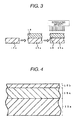
- Fig. 3 is a view for explaining a process for implanting impurity into the resist of a semiconductor substrate
- Fig. 4 is a view showing a state where impurity is implanted.
- an impurity introduction process involves coating a resist 16 on the semiconductor substrate 15a to form a mask, selectively patterning, and introducing impurity into the semiconductor substrate 15a with an impurity introduction apparatus, as shown in Fig. 3.
- the impurity is also introduced into the resist used as the mask, the surface is altered, so that a hardening layer 16b is formed, as shown in Fig. 4. Also, the inside of the resist is not affected by the impurity introduction process, and an nonhardening layer 16a in a state equivalent to the untreated resist.
- the film quality and film thickness of the hardening layer 16b depend on the dose and energy amount at the time of introducing impurity. In any way, the hardening layer 16b is firstly ashed and then the nonhardening layer 16a is ashed.
- this hardening layer 16b it is required that the semiconductor substrate 15a is placed at low temperature to decrease the ashing rate to prevent peeling off of the surface layer due to popping causing contamination of the semiconductor substrate 15a. That is, to lower the temperature, the temperature of a heater is decreased, and the very low ashing rate condition is required to avoid temperature rise due to plasma. To ash the nonhardening layer 16a after the hardening layer 16b is ashed, it is ideally required to increase the ashing rate by placing the semiconductor substrate at high temperature.
- Fig. 5 is a graph showing the luminous intensity of spectral light emitted from a reaction product during a low temperature processing and a high temperature processing.
- a change in the luminous intensity is smaller in the low temperature processing than the high temperature processing, whereby the interface between the resist 16 and the semiconductor substrate 15a can be detected, but it is difficult that the interface between the hardening layer 16b of resist with impurity implanted and the nonhardening layer 16a is detected.
- the thickness of the hardening layer is as thin as about 10nm, and it is more difficult to detect the interface between the hardening layer and the nonhardening layer.
- the hardening layer 16b and the nonhardening layer 16a had to be ashed at low temperature for enough time to suppress a pumping action. As a result, there is a problem that the ashing time is long and the throughput is remarkably low.
- a gas plasma in which helium gas is mixed into B 2 H 6 gas hydrogen and helium, besides boron, are necessarily implanted.
- a mixture ratio of B 2 H 6 gas and helium gas is typically 5% to 95%.
- boron of 1E15cm -2 is implanted, hydrogen of twice 1E15cm -2 is implanted, and helium of much more amount is implanted.
- the total amount of ions to be implanted is much greater in the latter case. For such reason, the surface hardening layer of resist is more easily formed by plasma doping.
- This invention discloses a measure for solving this problem.
- the desired impurity designates helium. If a large amount of helium ions are implanted, the surface hardening layer of resist is more easily formed.
- the problem with the use of plasma doping is peculiar to the plasma doping, unlike ion implantation, and has been found by the inventors for the first time.
- the plasma doping has a feature that the dose rate is higher by a few digits than the conventional ion implantation. Generally, it is said to be higher by three digits. Thereby, in the processing for the same period of time, an amount of ions, which is greater by three digits than the ion implantation, are implanted into silicon and resist.
- the processing time is extremely shorter by three digits, it is difficult to secure the uniformity and repeatability, which is unfavorable from the viewpoint of manufacturing. In this manner, the plasma doping had a peculiar problem.
- the invention provides an asher for plasma ashing a surface hardening layer formed on a resist and an internal nonhardening layer, the resist for use as a mask coated on a semiconductor substrate and doped with impurity, characterized by comprising an elipsometer for causing a linearly polarized light to enter the semiconductor substrate to detect a reflected, elliptically polarized light during plasma ashing, and detecting the interface between the hardening layer and the nonhardening layer and the interface between the nonhardening layer and the semiconductor substrate.
- the ashing of the nonhardening layer can be started by elevating the temperature to increase the ashing rate, whereby the throughput is increased. And if the end of ashing the nonhardening layer is detected, the ashing process is ended.
- the ashing process may be ended. And the removal of the nonhardening layer may be made by another process such as wet etching.
- the invention provides a method for analyzing the elipsometer, characterized by including detecting the reflected, elliptically polarized light and detecting the optical constants and the thickness of the hardening layer and the nonhardening layer.
- detecting the changes in the optical constants and the thickness of the hardening layer and the nonhardening layer the end time of ashing the hardening layer and the nonhardening layer can be predicted, whereby the throughput is increased and fed back to the ashing process at the same time.
- the asher comprises a feedback control mechanism for feeding the detected interface between the hardening layer and the nonhardening layer and interface between the hardening later and the semiconductor substrate, or the optical constants and the thickness of the hardening layer and the nonhardening layer back to the asher.
- the ions are implanted by plasma doping
- a high concentration of impurity is implanted onto the upper surface of the silicon substrate as compared with the ion implantation. Therefore, if the entire resist is removed by ashing, the upper surface of the silicon substrate is oxidized, whereby the impurity may not contribute to electrical conduction in some cases. Thus, the resist should be removed without oxidizing the surface as much as possible.
- the hardening layer of the resist is only removed by ashing, and the underlying nonhardening layer is removed by wet etching that is less likely to oxidize the silicon than the ashing, whereby the impurity is prevented from not contributing to electrical conduction. Also, it is desirable that its extent is reduced even if the impurity can not be prevented from not contributing.
- the elipsometer for detecting the interface between the hardening layer that is altered by impurity introduction and the internal nonhardening layer and the interface between the nonhardening layer and the semiconductor substrate is provided to change the ashing rate, whereby the ashing is made in a very short time without causing popping, so that the throughput is increased.
- the hardening layer that is altered by plasma doping and the internal nonhardening layer
- the hardening layer is removed by ashing and the nonhardening layer is removed by wet etching, whereby it is possible to prevent the impurity from not contributing to electrical conduction or reduce its extent.
- Fig. 1 is a typical cross-sectional view of an asher according to one embodiment of the invention.
- This asher comprises a chamber 8 into which an ashing gas is introduced and of which the pressure is reduced by a vacuum pump, an RF generator 1 for applying an RF power to an upper electrode 9 in this chamber 8, a stage 6, opposed to the upper electrode 9, serving as a lower electrode on which a wafer 3 is laid, and a heater 7, contained in this stage 6, for heating the wafer 3, as shown in Fig. 1.
- a light from a light source 2 is directed toward the surface of the wafer 3, and measured by a photometer 4, as shown in Fig. 1.
- the measurement result of the photometer 4 is sent to a control unit 5, and fed back to an ashing process.
- a method for detecting the interface between the hardening layer and the nonhardening layer and the interface between the nonhardening layer and the semiconductor substrate, or detecting the optical constants and the thickness of the hardening layer and the nonhardening layer will be described below.
- An Xe light outputted from an Xe light source 20 is converted into a linearly polarized light by a polarizer 21, and caused to be incident upon the substrate at an angle ⁇ 0 to the direction perpendicular to the substrate surface.
- the angle ⁇ 0 is a measured value from 45° to 90°.
- the axis of linearly polarized light for the incident light is inclined with respect to p direction (direction of the intersection between a plane vertical to the optical axis and a plane including the incident light and reflected light) and s direction (direction vertical to p direction within a plane vertical to the optical axis).
- the amplitude reflectance ratio between p and s components of the reflected light as elliptically polarized light is ⁇ and the phase difference between the p and s components is ⁇ .
- the reflected light as elliptically polarized light is passed through an analyzer 22 and caused to be incident on a spectrometer 23, where ⁇ and ⁇ are measured by a detector 24 while separating light into spectral components.
- the interface between the hardening layer and the nonhardening layer can be detected from the measurement results of the ellipsometer for ⁇ and ⁇ because the signals of ⁇ and ⁇ are different.
- the interface between the nonhardening layer and the semiconductor substrate can be detected from the measurement results of ellipsometer of ⁇ and ⁇ because the signals of ⁇ and ⁇ are different.
- a method for calculating not only the thickness but also the optical constants (refractive index n and extinction coefficient k) of the hardening layer and the nonhardening layer as unknown parameters from the ellipsometry measurement results of ⁇ and ⁇ by a least square method will be described below.
- the thickness and the optical constants (refractive index n and extinction coefficient k) of the hardening layer can be obtained, and it is detected whether or not the ashing process for the hardening layer is completed.
- the thickness and the optical constants (refractive index n and extinction coefficient k) of the nonhardening layer can be obtained, using a three layer model of Air/nonhardening layer/c-Si, and it is detected whether or not all the ashing process is completed.
- the optical constant has fundamentally the wavelength dependency. If the optical constant is measured by changing the wavelength, unknown parameters are increased by the number of measured wavelengths, whereby the optical constant can not be decided. In such a case, the spectrum of the optical constant is represented by an approximate expression including a constant not dependent on the wavelength, and the constant is made unknown parameter, whereby the spectrum of the optical constant can be obtained.
- the Tauc-Lorentz analysis, Cody-Lorentz analysis, Forouhi-Bloomer analysis, MDF analysis, band analysis, Tetrahedral analysis, Drude analysis and Lorentz analysis methods may be employed for the refractive index wavelength dispersion model to make the above analysis.
- E Photon Energy (eV)
- ⁇ wavelength
- f(E) is the integral value of the expression (2-2) and C5 is an integration constant.
- C1, C2, C3, C4 and C5 are parameters, and initial values.
- C5 is the integration constant, and one of the parameters representing the refractive index, whereby the refractive index of the hardening layer is set to a round number as the initial value.
- C1 is a substantial extinction coefficient. That is, the value of extinction coefficient at the peak of extinction coefficient spectrum is the initial value.
- C2 and C3 have the relation with E(eV) at the peak of the extinction coefficient spectrum, in which the initial value of C2 is set to double E(eV) at the peak and the initial value of C3 is set to the square of E(eV) at the peak.
- C4 has the relation with the energy band width of absorption band, in which the initial value of C4 is equal to the value of E(eV) at which the extinction coefficient is smallest at the tail of the peak of extinction coefficient spectrum.
- the initial value can be set, supposing the absorption spectrum, or the extinction coefficient spectrum, including the physical properties of the thin film that is measurement object matter, thereby making the analysis.
- the optical constants and the thickness of the hardening layer and the nonhardening layer can be detected by the above method. And the end time of ashing the hardening layer and the nonhardening layer can be predicted, whereby the throughput is increased. At the same time, the ashing process can be fed back.
- the pressure of the chamber 8 is reduced in a state where the wafer 3 is laid on the stage 6. If a predetermined pressure is reached, the chamber is evacuated to vacuum while an oxygen gas that is etching gas is introduced, so that the internal pressure of the chamber 8 is kept at a fixed pressure. On the other hand, the wafer 3 is maintained at low temperature by setting the temperature of the heater 7.
- an RF power at low ashing rate is applied to generate an oxygen plasma and start the ashing.
- ⁇ and ⁇ are measured using the ellipsometer.
- the hardening layer is ashed, whereby the RF power is increased, for example, 1.5 times to make the ashing rate higher, and the ashing is performed.
- the nonhardening layer of the resist is ashed at a high ashing rate earlier than conventionally, whereby the overall ashing time is shortened.
- the thickness of the hardening layer reaches zero while monitoring the optical constants and the thickness of the hardening layer, it is determined that the hardening layer is ashed, whereby the RF power is increased, for example, 1.5 times to make the ashing rate higher and the ashing is performed.
- the nonhardening layer of the resist is ashed at the high ashing rate earlier than conventionally, whereby the overall ashing time is shortened.
- the thickness and optical constants (refractive index n and extinction coefficient k) of the nonhardening layer are detected, and it is detected whether or not all the ashing process is completed. And if all the ashing process is completed, the ashing is ended.
- the temperature of the wafer 3 may be changed if means for heating the wafer 3 is a lamp. Besides, the mixture ratio of oxygen gas and Freon gas may be changed.
- the doping and ashing process can be completed within the apparatus of a so-called multi-chamber in which a plurality of plasma chambers are provided. Or one series of impurity doping processes may be performed in an apparatus group for performing the consecutive processes, though they are disposed as separate apparatuses for the sake of convenience.
- a crystalline layer on the surface of a silicon substrate 109 was made amorphous, using a helium gas plasma.
- Fig. 6 is a cross-sectional view of a plasma doping chamber in a plasma doping apparatus for use in an embodiment 2 of the invention.
- a predetermined gas is introduced from a gas supply apparatus 102 into a vacuum vessel 101, which is then evacuated by a turbo molecular pump 103 as an evacuator, so that the vacuum vessel 101 can be kept at a predetermined pressure by a pressure governing valve 104.
- An inductive coupled plasma can be generated within the vacuum vessel 101 by supplying an RF power of 13.56MHz from an RF generator 105 to a coil 108 provided near a dielectric window 107 opposed to a sample electrode 106.
- the silicon substrate 109 as a sample is laid on the sample electrode 106.
- an RF generator 110 for supplying the RF power to the sample electrode 106 is provided to function as a voltage source for controlling the potential of the sample electrode 106 so that the substrate 109 as the sample may have a negative potential to the plasma. In this manner, ions in the plasma are accelerated toward the surface of the sample to collide with it to make the surface of the sample amorphous or introduce the impurity.
- the gas supplied from the gas supply apparatus 102 is exhausted out of an exhaust port 111 into a pump 103.
- the turbo molecular pump 103 and the exhaust port 111 are placed directly under the sample electrode 106.
- the pressure governing valve 104 is a lift valve located directly under the sample electrode 106 and directly above the turbo molecular pump 103.
- the sample electrode 106 is fixed to the vacuum vessel 101 by four struts 112.
- the vacuum vessel 101 is evacuated out of the exhaust port 111 while the temperature of the sample electrode 106 is kept at 25°C. Then, a helium gas of 50sccm is supplied from the gas supply apparatus 102 into the vacuum vessel 101, and the pressure of the vacuum vessel 101 is kept at 1 Pa by controlling the pressure governing valve 104. Then, a plasma is generated within the vacuum vessel 101 by supplying an RF power of 800W to the coil 108 as a plasma source, and the crystalline layer on the surface of the silicon substrate 109 is made amorphous by supplying an RF power of 200W to a base of the sample electrode 106. The exposure time to the helium plasma is 7 seconds.
- a resist is patterned on the surface of the silicon substrate 109. Some part of the surface of the silicon substrate is exposed from a gap in the resist. After the amorphous treatment, boron of 3E14cm -2 was implanted by ion implantation. The hardening layer was present on the surface of resist. The hardening layer of resist was removed by ashing. Thereafter, the nonhardening layer 16a was removed by wet etching. Thereafter, the activation process was performed with spike RTA at 1070°C to measure the sheet resistance.
- helium implanted into the silicon substrate was 1E16cm -2 . It is considered that the hardening layer on the resist surface is formed by plasma doping of helium.
- a solid silicon substrate without resist pattern was prepared, made amorphous by helium plasma, and doped with boron by ion implantation, whereby the activation process was performed with spike RTA at 1070°C to measure the sheet resistance.
- the sheet resistance was equivalent to the sheet resistance in the case where after the hardening layer of resist was removed by ashing, the nonhardening layer 16a was removed by wet etching.
- a silicon substrate with the patterned resist was made amorphous by helium plasma and doped with boron by ion implantation, whereby after the entire resist was removed by ashing, the activation process was performed with spike RTA at 1070°C to measure the sheet resistance.
- the sheet resistance was greater than the sheet resistance in the case where after the hardening layer of resist was removed by ashing, the nonhardening layer 16a was removed by wet etching. It is considered that the percentage of impurity not contributing to electrical conduction is increased.
- a silicon substrate was doped with boron by plasma doping using a mixed gas plasma of B 2 H 6 and He.
- a plasma doping chamber of a plasma doping apparatus of Fig. 6 used in the embodiment 2 of the invention is used.
- a vacuum chamber 101 is evacuated by a turbo molecular pump 103 as an evacuator while a predetermined gas is introduced from a gas supply apparatus 102 into the vacuum vessel 101, so that the vacuum chamber 101 can be kept at a predetermined pressure by a pressure governing valve 104.
- a pressure governing valve 104 By supplying an RF power of 13.56MHz from an RF generator 105 to a coil 108 provided near a dielectric window 107 opposed to a sample electrode 106, an inductive coupled plasma can be generated within the vacuum vessel 101.
- the silicon substrate 109 as a sample is laid on the sample electrode 106.
- an RF generator 110 for supplying RF power to the sample electrode 106 is provided to function as a voltage source for controlling the potential of the sample electrode 106 so that the substrate 109 as the sample may have a negative potential to the plasma. In this manner, ions in the plasma are accelerated toward the surface of the sample to collide with it to make the surface of the sample amorphous or introduce the impurity.
- the gas supplied from the gas supply apparatus 102 is exhausted out of an exhaust port 111 into a pump 103.
- the turbo molecular pump 103 and the exhaust port 111 are placed directly under the sample electrode 106.
- the pressure governing valve 104 is a lift valve located directly under the sample electrode 106 and directly above the turbo molecular pump 103.
- the sample electrode 106 is a base of almost square shape on which the substrate 109 is laid, and fixed to the vacuum vessel 101 by a strut 112 on each side, or by a total of four struts 112.
- a plasma was generated within the vacuum vessel 101 by supplying helium (He) gas of 97sccm and B 2 H 6 gas of 3sccm into the vacuum vessel 1 while the temperature of the sample electrode 106 is kept at 25°C, and by supplying an RF power of 1000W to the coil 108 while the pressure of the vacuum vessel 1 is kept at 0.9Pa, and boron was introduced near the surface of the substrate 109 by supplying an RF power of 250W to the sample electrode 106.
- the gas mixture ratio was equivalent to B 2 H 6 3% to He 97%.
- the plasma-doping time was adjusted so that the dose of boron into the silicon substrate might be 1E14cm -2 .
- the resist is patterned on the surface of the silicon substrate 109. Some part of the surface of the silicon substrate is exposed from a gap in the resist.
- the hardening layer was present on the surface of resist after plasma doping.
- the hardening layer of resist was removed by ashing. Thereafter, the nonhardening layer 16a was removed by wet etching. Thereafter, the activation process was performed with spike RTA at 1070°C to measure the sheet resistance.
- boron implanted into the silicon substrate was 1E14cm -2 .
- hydrogen of 3E14cm -2 and helium of 4E15cm -2 were implanted. It is considered that the hardening layer on the resist surface is formed by plasma doping of helium. If the mixture ratio of helium gas is 97% or more, more amount of helium is implanted than boron, so that the hardening layer on the resist surface is more easily formed. Also, if boron of 1E14cm -2 or more is implanted, helium is increased along with increased dose of boron, so that the hardening layer on the resist surface is more easily formed.
- a solid silicon substrate without resist pattern was prepared, boron was implanted by plasma doping, and the activation process was performed with spike RTA at 1070°C to measure the sheet resistance.
- the sheet resistance was equivalent to the sheet resistance in the case where after the hardening layer of the resist was removed by ashing, the nonhardening layer 16a was removed by wet etching.
- boron was implanted into a silicon substrate with patterned resist by plasma doping, and after the entire resist was removed only by ashing, the activation process with spike RTA at 1070°C was performed to measure the sheet resistance.
- the sheet resistance was greater than where after the hardening layer of the resist was removed by ashing, the nonhardening layer 16a was removed by wet etching. It is considered that the percentage of impurity not contributing to electrical conduction was increased.
- the asher, the ashing method and the impurity doping apparatus group of the invention are effective to form the electronic devices such as condenser, varistor, diode, transistor and coil, because it is possible to detect the interface between the surface hardening layer of the resist after impurity doping and the internal nonhardening layer and the interface between the nonhardening layer and the semiconductor substrate, whereby the throughput of ashing is increased.
Landscapes
- Physics & Mathematics (AREA)
- Engineering & Computer Science (AREA)
- Plasma & Fusion (AREA)
- Chemical & Material Sciences (AREA)
- Analytical Chemistry (AREA)
- Drying Of Semiconductors (AREA)
- Exposure Of Semiconductors, Excluding Electron Or Ion Beam Exposure (AREA)
Applications Claiming Priority (2)
| Application Number | Priority Date | Filing Date | Title |
|---|---|---|---|
| JP2005099148 | 2005-03-30 | ||
| PCT/JP2006/306740 WO2006106871A1 (fr) | 2005-03-30 | 2006-03-30 | Appareil de cendrage, procédé de cendrage et appareil de dopage des impuretés |
Publications (2)
| Publication Number | Publication Date |
|---|---|
| EP1865547A1 true EP1865547A1 (fr) | 2007-12-12 |
| EP1865547A4 EP1865547A4 (fr) | 2010-01-13 |
Family
ID=37073426
Family Applications (1)
| Application Number | Title | Priority Date | Filing Date |
|---|---|---|---|
| EP06730688A Withdrawn EP1865547A4 (fr) | 2005-03-30 | 2006-03-30 | Appareil de cendrage, procédé de cendrage et appareil de dopage des impuretés |
Country Status (6)
| Country | Link |
|---|---|
| US (1) | US20090104783A1 (fr) |
| EP (1) | EP1865547A4 (fr) |
| JP (1) | JPWO2006106871A1 (fr) |
| KR (1) | KR20080005190A (fr) |
| CN (1) | CN100511599C (fr) |
| WO (1) | WO2006106871A1 (fr) |
Families Citing this family (6)
| Publication number | Priority date | Publication date | Assignee | Title |
|---|---|---|---|---|
| JP5027066B2 (ja) * | 2008-06-27 | 2012-09-19 | ルネサスエレクトロニクス株式会社 | 半導体集積回路装置の製造方法 |
| JPWO2010150315A1 (ja) * | 2009-06-25 | 2012-12-06 | パイオニア株式会社 | 光ディスクの製造方法および光ディスクの製造ライン |
| JP2012114157A (ja) * | 2010-11-22 | 2012-06-14 | Toshiba Corp | ドロップレシピ作成方法およびデータベース作成方法 |
| JP6681061B2 (ja) * | 2015-05-08 | 2020-04-15 | 公立大学法人大阪 | レジスト剥離方法およびレジスト剥離装置 |
| JP7099897B2 (ja) * | 2018-07-23 | 2022-07-12 | 株式会社アルバック | ドライエッチング方法 |
| CN119511654A (zh) * | 2023-08-23 | 2025-02-25 | 北京北方华创微电子装备有限公司 | 晶圆上光刻胶的去除方法及半导体工艺设备 |
Family Cites Families (14)
| Publication number | Priority date | Publication date | Assignee | Title |
|---|---|---|---|---|
| US3824017A (en) * | 1973-03-26 | 1974-07-16 | Ibm | Method of determining the thickness of contiguous thin films on a substrate |
| JPH01232202A (ja) * | 1988-03-14 | 1989-09-18 | Teru Kyushu Kk | 膜厚測定方法 |
| JP3698266B2 (ja) * | 1995-12-28 | 2005-09-21 | 富士通株式会社 | 半導体装置の製造方法および半導体装置の製造装置 |
| US6128084A (en) * | 1997-06-11 | 2000-10-03 | Matsushita Electronics Corporation | Evaluation method of semiconductor layer, method for fabricating semiconductor device, and storage medium |
| JP3848833B2 (ja) * | 1997-06-11 | 2006-11-22 | 松下電器産業株式会社 | 半導体層の評価方法及び半導体装置の製造方法 |
| JP2001274139A (ja) * | 2000-03-23 | 2001-10-05 | Nec Corp | アッシング装置およびアッシング方法 |
| US6462817B1 (en) * | 2000-05-12 | 2002-10-08 | Carlos Strocchia-Rivera | Method of monitoring ion implants by examination of an overlying masking material |
| US6989900B1 (en) * | 2001-04-02 | 2006-01-24 | Advanced Micro Devices, Inc. | Method of measuring implant profiles using scatterometric techniques |
| US6585908B2 (en) * | 2001-07-13 | 2003-07-01 | Axcelis Technologies, Inc. | Shallow angle interference process and apparatus for determining real-time etching rate |
| JP4544447B2 (ja) * | 2002-11-29 | 2010-09-15 | パナソニック株式会社 | プラズマドーピング方法 |
| US20040195208A1 (en) * | 2003-02-15 | 2004-10-07 | Pavel Elizabeth G. | Method and apparatus for performing hydrogen optical emission endpoint detection for photoresist strip and residue removal |
| JP4694150B2 (ja) * | 2003-06-20 | 2011-06-08 | 東京エレクトロン株式会社 | 処理方法及び処理システム |
| JP2005064197A (ja) * | 2003-08-11 | 2005-03-10 | Seiko Epson Corp | レジスト膜のアッシング方法及びそのアッシング条件算出システム、並びに、レジスト膜のアッシング装置 |
| US7821655B2 (en) * | 2004-02-09 | 2010-10-26 | Axcelis Technologies, Inc. | In-situ absolute measurement process and apparatus for film thickness, film removal rate, and removal endpoint prediction |
-
2006
- 2006-03-30 US US11/887,457 patent/US20090104783A1/en not_active Abandoned
- 2006-03-30 EP EP06730688A patent/EP1865547A4/fr not_active Withdrawn
- 2006-03-30 JP JP2007512891A patent/JPWO2006106871A1/ja active Pending
- 2006-03-30 WO PCT/JP2006/306740 patent/WO2006106871A1/fr not_active Ceased
- 2006-03-30 CN CNB2006800103389A patent/CN100511599C/zh not_active Expired - Fee Related
- 2006-03-30 KR KR1020077021859A patent/KR20080005190A/ko not_active Withdrawn
Also Published As
| Publication number | Publication date |
|---|---|
| KR20080005190A (ko) | 2008-01-10 |
| JPWO2006106871A1 (ja) | 2008-09-11 |
| US20090104783A1 (en) | 2009-04-23 |
| EP1865547A4 (fr) | 2010-01-13 |
| WO2006106871A1 (fr) | 2006-10-12 |
| CN101151715A (zh) | 2008-03-26 |
| CN100511599C (zh) | 2009-07-08 |
Similar Documents
| Publication | Publication Date | Title |
|---|---|---|
| EP1098189B1 (fr) | Méthode de détection du point d'achèvement d'un traitement par plasma en l'absence d'oxygène | |
| US6462817B1 (en) | Method of monitoring ion implants by examination of an overlying masking material | |
| US6916396B2 (en) | Etching system and etching method | |
| US8778205B2 (en) | Processing method and processing system | |
| US20070221620A1 (en) | Processes for monitoring the levels of oxygen and/or nitrogen species in a substantially oxygen and nitrogen-free plasma ashing process | |
| US20040195208A1 (en) | Method and apparatus for performing hydrogen optical emission endpoint detection for photoresist strip and residue removal | |
| Thomas III et al. | Monitoring InP and GaAs etched in Cl2/Ar using optical emission spectroscopy and mass spectrometry | |
| EP1865547A1 (fr) | Appareil de cendrage, procédé de cendrage et appareil de dopage des impuretés | |
| US6340603B1 (en) | Plasma emission detection during lateral processing of photoresist mask | |
| Sin et al. | Resist trimming in high-density CF 4/O 2 plasmas for sub-0.1 μm device fabrication | |
| WO2005031832A1 (fr) | Procede d'introduction d'impurete, appareil d'introduction d'impurete et dispositif electronique produit au moyen de ces derniers | |
| WO2010110878A1 (fr) | Procédé de gravure au plasma | |
| US20130071955A1 (en) | Plasma etching method | |
| JPH1187448A5 (fr) | ||
| US6265316B1 (en) | Etching method | |
| US12237174B2 (en) | Etching method | |
| Pang et al. | Laser-Induced Fluorescence Diagnostics of CF4/O2/H2 Plasma Etching | |
| Leonhardt et al. | Surface chemistry and damage in the high density plasma etching of gallium arsenide | |
| JP4018829B2 (ja) | 半導体装置の製造方法 | |
| JP2001274139A (ja) | アッシング装置およびアッシング方法 | |
| Eriguchi et al. | Quantitative characterization of plasma-induced defect generation process in exposed thin Si surface layers | |
| Jang Jian et al. | Visualization of plasma etching damage of Si using room temperature spectroscopic photoluminescence | |
| Iwakoshi et al. | Prediction of etching results and etching stabilization by applying principal component regression to emission spectra during in-situ cleaning | |
| Murtagh et al. | Photoreflectance Characterisation of Reactive Ion Etched Silicon | |
| Gumprecht et al. | Measurement strategy for dielectric ultra-thin film characterization by vacuum ultra-violet reflectometry |
Legal Events
| Date | Code | Title | Description |
|---|---|---|---|
| PUAI | Public reference made under article 153(3) epc to a published international application that has entered the european phase |
Free format text: ORIGINAL CODE: 0009012 |
|
| 17P | Request for examination filed |
Effective date: 20070926 |
|
| AK | Designated contracting states |
Kind code of ref document: A1 Designated state(s): DE FR GB |
|
| DAX | Request for extension of the european patent (deleted) | ||
| RBV | Designated contracting states (corrected) |
Designated state(s): DE FR GB |
|
| RAP1 | Party data changed (applicant data changed or rights of an application transferred) |
Owner name: PANASONIC CORPORATION |
|
| A4 | Supplementary search report drawn up and despatched |
Effective date: 20091210 |
|
| STAA | Information on the status of an ep patent application or granted ep patent |
Free format text: STATUS: THE APPLICATION HAS BEEN WITHDRAWN |
|
| 18W | Application withdrawn |
Effective date: 20100129 |