EP1865592A1 - Alimentation à découpage - Google Patents
Alimentation à découpage Download PDFInfo
- Publication number
- EP1865592A1 EP1865592A1 EP06425378A EP06425378A EP1865592A1 EP 1865592 A1 EP1865592 A1 EP 1865592A1 EP 06425378 A EP06425378 A EP 06425378A EP 06425378 A EP06425378 A EP 06425378A EP 1865592 A1 EP1865592 A1 EP 1865592A1
- Authority
- EP
- European Patent Office
- Prior art keywords
- voltage
- integrated
- switched
- switch
- electrical
- Prior art date
- Legal status (The legal status is an assumption and is not a legal conclusion. Google has not performed a legal analysis and makes no representation as to the accuracy of the status listed.)
- Granted
Links
- 239000004065 semiconductor Substances 0.000 claims abstract description 9
- 238000004804 winding Methods 0.000 claims description 14
- VYPSYNLAJGMNEJ-UHFFFAOYSA-N Silicium dioxide Chemical compound O=[Si]=O VYPSYNLAJGMNEJ-UHFFFAOYSA-N 0.000 claims description 11
- 238000002955 isolation Methods 0.000 claims description 11
- 229910021420 polycrystalline silicon Inorganic materials 0.000 claims description 8
- 230000015556 catabolic process Effects 0.000 claims description 5
- 235000012239 silicon dioxide Nutrition 0.000 claims description 5
- 239000000377 silicon dioxide Substances 0.000 claims description 5
- 230000005669 field effect Effects 0.000 claims description 4
- 239000000758 substrate Substances 0.000 claims description 4
- 229910044991 metal oxide Inorganic materials 0.000 claims description 3
- 150000004706 metal oxides Chemical class 0.000 claims description 3
- 239000000463 material Substances 0.000 claims description 2
- 239000004020 conductor Substances 0.000 claims 1
- 230000002093 peripheral effect Effects 0.000 claims 1
- 238000000034 method Methods 0.000 description 8
- 230000010354 integration Effects 0.000 description 7
- 238000001465 metallisation Methods 0.000 description 7
- 239000003990 capacitor Substances 0.000 description 6
- 238000005516 engineering process Methods 0.000 description 6
- 239000007943 implant Substances 0.000 description 5
- XUIMIQQOPSSXEZ-UHFFFAOYSA-N Silicon Chemical compound [Si] XUIMIQQOPSSXEZ-UHFFFAOYSA-N 0.000 description 3
- 238000010586 diagram Methods 0.000 description 3
- 238000004519 manufacturing process Methods 0.000 description 3
- 229910052710 silicon Inorganic materials 0.000 description 3
- 239000010703 silicon Substances 0.000 description 3
- 239000005380 borophosphosilicate glass Substances 0.000 description 2
- 238000009792 diffusion process Methods 0.000 description 2
- 239000011521 glass Substances 0.000 description 2
- 239000002184 metal Substances 0.000 description 2
- 238000002161 passivation Methods 0.000 description 2
- MXSJNBRAMXILSE-UHFFFAOYSA-N [Si].[P].[B] Chemical compound [Si].[P].[B] MXSJNBRAMXILSE-UHFFFAOYSA-N 0.000 description 1
- 230000009286 beneficial effect Effects 0.000 description 1
- 230000015572 biosynthetic process Effects 0.000 description 1
- 230000000295 complement effect Effects 0.000 description 1
- 238000007796 conventional method Methods 0.000 description 1
- 230000010485 coping Effects 0.000 description 1
- 230000001419 dependent effect Effects 0.000 description 1
- 238000000151 deposition Methods 0.000 description 1
- 230000008021 deposition Effects 0.000 description 1
- 238000009499 grossing Methods 0.000 description 1
- 239000012212 insulator Substances 0.000 description 1
- 230000003287 optical effect Effects 0.000 description 1
- 229920005591 polysilicon Polymers 0.000 description 1
- 239000011347 resin Substances 0.000 description 1
- 229920005989 resin Polymers 0.000 description 1
- 230000000087 stabilizing effect Effects 0.000 description 1
Images


Classifications
-
- H—ELECTRICITY
- H02—GENERATION; CONVERSION OR DISTRIBUTION OF ELECTRIC POWER
- H02M—APPARATUS FOR CONVERSION BETWEEN AC AND AC, BETWEEN AC AND DC, OR BETWEEN DC AND DC, AND FOR USE WITH MAINS OR SIMILAR POWER SUPPLY SYSTEMS; CONVERSION OF DC OR AC INPUT POWER INTO SURGE OUTPUT POWER; CONTROL OR REGULATION THEREOF
- H02M1/00—Details of apparatus for conversion
- H02M1/36—Means for starting or stopping converters
-
- H—ELECTRICITY
- H02—GENERATION; CONVERSION OR DISTRIBUTION OF ELECTRIC POWER
- H02M—APPARATUS FOR CONVERSION BETWEEN AC AND AC, BETWEEN AC AND DC, OR BETWEEN DC AND DC, AND FOR USE WITH MAINS OR SIMILAR POWER SUPPLY SYSTEMS; CONVERSION OF DC OR AC INPUT POWER INTO SURGE OUTPUT POWER; CONTROL OR REGULATION THEREOF
- H02M3/00—Conversion of DC power input into DC power output
- H02M3/22—Conversion of DC power input into DC power output with intermediate conversion into AC
- H02M3/24—Conversion of DC power input into DC power output with intermediate conversion into AC by static converters
- H02M3/28—Conversion of DC power input into DC power output with intermediate conversion into AC by static converters using discharge tubes with control electrode or semiconductor devices with control electrode to produce the intermediate AC
- H02M3/325—Conversion of DC power input into DC power output with intermediate conversion into AC by static converters using discharge tubes with control electrode or semiconductor devices with control electrode to produce the intermediate AC using devices of a triode or a transistor type requiring continuous application of a control signal
- H02M3/335—Conversion of DC power input into DC power output with intermediate conversion into AC by static converters using discharge tubes with control electrode or semiconductor devices with control electrode to produce the intermediate AC using devices of a triode or a transistor type requiring continuous application of a control signal using semiconductor devices only
- H02M3/33507—Conversion of DC power input into DC power output with intermediate conversion into AC by static converters using discharge tubes with control electrode or semiconductor devices with control electrode to produce the intermediate AC using devices of a triode or a transistor type requiring continuous application of a control signal using semiconductor devices only with automatic control of the output voltage or current, e.g. flyback converters
-
- Y—GENERAL TAGGING OF NEW TECHNOLOGICAL DEVELOPMENTS; GENERAL TAGGING OF CROSS-SECTIONAL TECHNOLOGIES SPANNING OVER SEVERAL SECTIONS OF THE IPC; TECHNICAL SUBJECTS COVERED BY FORMER USPC CROSS-REFERENCE ART COLLECTIONS [XRACs] AND DIGESTS
- Y10—TECHNICAL SUBJECTS COVERED BY FORMER USPC
- Y10S—TECHNICAL SUBJECTS COVERED BY FORMER USPC CROSS-REFERENCE ART COLLECTIONS [XRACs] AND DIGESTS
- Y10S323/00—Electricity: power supply or regulation systems
- Y10S323/901—Starting circuits
Definitions
- the present invention relates to switched-mode electronic power devices, in which integrated circuits are used for driving high-voltage switches and in which a start-up circuit is also required to be used.
- SMPS Switched Mode Power Supplies
- the patent US-A-5313381 describes, with reference to the prior art, an SMPS power supply comprising a rectifier and an input filter connected to a primary of a transformer.
- the secondary of this transformer is connected to a rectifier and an output filter being provided with terminals in order to supply a load with a direct voltage.
- the primary of the transformer is connected to a MOSFET (Metal Oxide Semiconductor Field Effect Transistor) switch that is intended to be driven by a PWM (Pulse Width Modulation) controller.
- MOSFET Metal Oxide Semiconductor Field Effect Transistor
- PWM Pulse Width Modulation
- the PWM is caused to operate by a start-up network, which can be deactivated after the start-up has been carried out, based on the particular type of application.
- a suitable performance/cost ratio is particularly difficult to achieve when manufacturing these switched-mode devices. This is mainly due to the fact that these devices have high-voltage components, such as the switching MOSFET and several components of the start-up network, and components that can be low-voltage (typically the PWM controller).
- the object of the present invention is to provide a switched-mode electronic power device alternative to those of the prior art, and which overcomes the above-mentioned drawbacks of the conventional devices.
- the object of the present invention is achieved by a switched-mode electronic power device such as defined in claim 1. Preferred embodiments thereof are as described in the dependent claims 2 to 20.
- the object of the present invention is also an electrical apparatus including said device such as described in the annexed claim 21 and preferred embodiments thereof such as defined in claims 22 to 24.
- Fig. 1 shows an apparatus 1 provided according to a first embodiment of the present invention.
- the apparatus 1 is a switched-mode power supply, which is known to those skilled in the art with the name of SMPS (Switch Mode Power Supply).
- SMPS Switch Mode Power Supply
- the present invention can also be applied to apparatuses other than the switched-mode power supply described in this particular embodiment.
- the power supply 1 comprises a switched-mode electronic power supply 2, which controls an isolation transformer 3 interposed between an input circuit 4 (which is supplied by an alternated voltage generator V AC ) and an output circuit 5 provided with terminals 7 for connection to an external load (not shown).
- the output circuit 5 is connected to the power device 2 by means of a feedback block 6.
- the electronic power device 2 comprises a high-voltage switch 8, such as a change-over switch or power switch that can be provided, particularly, by means of, preferably, an N-channel MOSFET transistor.
- the MOSFET transistor 8 (called the PMOS power switch 8 herein below) has a terminal connected to the transformer 3.
- the electronic power device 2 is further provided with a low-voltage block 9 for driving the PMOS power switch 8, such as a PWM (Pulse Width Modulation) modulator that can be preferably provided by means of a miniaturized controller.
- a PWM (Pulse Width Modulation) modulator that can be preferably provided by means of a miniaturized controller.
- a turn-on or start-up circuit 10 is also included in the electronic power device 2, which can be made by conventional techniques, and such as to be enabled to operation during a start-up step of the device 2 and apparatus 1, and is then disabled during the normal "work" of the device 2.
- the start-up circuit 10 activates the PWM driving block 9, which, in turn, activates the PMOS power switch 8.
- the start-up circuit 10 is provided with a high-voltage resistor 15 that is intended to be connected to the PWM driving block 9 which, on the other hand, operates under low voltage.
- this resistor 15 has such a resistance - 100 kOhm to 100 MegaOhm, according to what is required by the particular PWM driving block 9 - which is sufficiently high to cause a potential drop at the ends thereof, due to which the driving block is not subjected to the high voltages at which the start-up circuit 10 operates, and which may damage it.
- the input circuit 4 comprises a rectifier 11, such as a diode bridge connected to an input filter 12, which includes, particularly, a smoothing capacitor.
- the input filter 12 is connected to a first winding of the transformer 3, the second winding thereof being connected to the output circuit 5.
- the output circuit 5 comprises an output rectifier 13 (such as a rectifier diode) connected to an output filter 14.
- the feedback block 6 comprises, preferably, a conventional optical insulator which couples the output filter 14 to the PWM driving block 9 such as to avoid a direct electrical contact.
- this can be manufactured by means of conventional integration techniques, such as preferably silicon integration techniques, and particularly, using the PMOS technology for the start-up circuit 10 and the power switch 8 and Bi-CMOS (Bipolar Complementary MOS) for the PWM driving block 9.
- conventional integration techniques such as preferably silicon integration techniques, and particularly, using the PMOS technology for the start-up circuit 10 and the power switch 8 and Bi-CMOS (Bipolar Complementary MOS) for the PWM driving block 9.
- start-up circuit 10 (comprising the high-voltage resistor 15) and the PMOS power switch 8 are integrated in a same chip 16, and the PWM driving block 9 is integrated in a different and separated second chip 17, and is connected to the first chip 16 by means of conductive wires (not shown), suitably extending between the two chips.
- first chip 16 and second chip 17 are housed in a same enclosure or package 18 that can be made with conventional materials and techniques.
- the first chip 16 and the second chip 17 are fixed to two electrically-isolated conductive bases of package 18 (such as made of a resin known to those skilled in the art) which is provided with feet 19 for connection to external circuit elements, such as the circuit blocks of apparatus 1.
- the electronic device 2 is thus “hybrid”, because it includes both high-voltage components (the first chip 16 is a “power” circuit) and low-voltage components (the second chip 17 is a “signal” circuit), even though these are integrated in different semiconductor chip.
- high-voltage and low-voltage are known to those skilled in the art to differentiate two devices based on the typology to which they belong. Particularly, these terms can also relate to the type of application, i.e. power applications (high-voltage) and signal application (low-voltage) and not only to the difference between the operative voltages of the compared devices.
- the first chip 16 operates, for example, from 300 V to 1700 V, whereas the second chip 17 operates, for example, at voltages lower than 100 V.
- a capacitor C1 external to the electronic device 2 which acts as a power supply for the PWM driving block 9 and is also connected to the start-up circuit 10 and to an auxiliary winding of the transformer 3 (not shown in the figure).
- Fig. 3 shows the equivalent electrical diagram of a particular embodiment of the start-up circuit 10 and PMOS power switch 8 to be integrated in the first chip 16.
- the PMOS power switch 8 (represented with the symbol that also shows the inherent recirculation diode) has a first drain terminal D1 to be connected to the primary winding of the transformer 3, a first gate terminal G1, a first source terminal S1, both to be connected to respective terminals of the PWM driving block 9.
- the start-up circuit 10 comprises a switching circuit 20 having the function of allowing the start-up circuit to adopt an active configuration, during the step of starting up the power supply 1, in order to take a turn-on electrical signal to be supplied to the capacitor C1 thereby allowing the operation of the PWM driving block 9, which in turn can drive the PMOS power switch 8 and, subsequently, adopt a passive configuration in which the capacitor C1 is not supplied, which is, on the other hand, loaded by the auxiliary winding of the transformer.
- This switching circuit 20 includes the high-voltage resistor 15, a further PMOS power switch 21 and a threshold circuit that is made, for example, with a Zener diode chain DZ1 and DZN in a back-to-back configuration (a pair of which is depicted).
- the further power switch 21 is provided with a second drain terminal D2 common to the first drain terminal D1, a second gate terminal G2 and a second source terminal S2.
- the high-voltage resistor 15 is interposed between a cathode of a Zener diode DZ1 and the drain terminals D1 and D2 of the PMOS power switches 8 and 21.
- the second gate terminal G2 and the second source terminal S2 are intended to be connected to corresponding terminals of the PWM driving block 9.
- the alternated-voltage generator V AC supplies the rectifier 11 and the input filter 12.
- the thus-obtained rectified current supplies the primary winding of the transformer 3. If the PMOS power switch 8 is open, the current does not flow within the primary winding of the primary winding of the transformer 3, and thus the PWM driving block 9 connected thereto is not supplied and is not activated.
- the start-up circuit 10 connected to the primary winding of the transformer 3 turns to the active state when the voltage of this primary winding exceeds the block voltage of the diode chain DZ1 and DZN.
- the diode chain DZ1 and DZN is in the conduction state thereby causing the current to flow in the high-voltage resistor 15.
- the further PMOS power switch 21 acts as a current generator, by loading the external capacitor C1, which acts as the power supply for the PWM driving block 9.
- the PWM driving block 9 is thus operated and drives the PMOS power switch 8, which switches according to a trend fixed by the PWM block 9, and i.e. based on a width-modulated train of pulses.
- the high-voltage resistor 15 avoids that the PWM driving block 9 is subjected to high voltage values, which are, on the other hand, applied to the PMOS 21 and PMOS 8 switches.
- the current affecting the primary winding of the transformer 3, modulated by the PMOS power switch 8, generates a corresponding alternated signal on the output circuit 5.
- the output rectifier 13 and the output filter 14 provide the terminals 7 and thus the external load with a direct voltage of a suitable level.
- the feedback block 6 takes a feedback signal from the output filter 14, which is supplied to the PWM driving block 9.
- the charge of the supply capacitor C1 causes the PWM driving block 9 to provide the start-up circuit 10 (for example, at the second gate terminal G2) with a voltage that causes the further power switch 21 to shift to an open state (i.e. not in conduction).
- the start-up circuit 10 is deactivated (the PMOS 21 is open), and the power switch PMOS 8 is switched under the control of only the PWM driving block 9.
- the consumption under normal running conditions of the electronic device 2 is conveniently small when a high-voltage resistor 15 is selected which has a sufficiently high resistance.
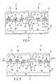
- Fig. 4 a portion of the first chip 16 is shown, in which the PMOS power switch 8 and the further PMOS power switch 21 are integrated.
- the two PMOS switches in Fig. 4 are identical to each other and can be provided by means of conventional silicon integration techniques, which typically provide using photolithographic steps, deposition steps, implant and diffusion steps for forming differently doped silicon layers, polycrystalline silicon layers, silicon dioxide layers and metallization layers.
- the PMOS 8 and PMOS 21 power switches are vertical, as is usual with power MOSes, and comprise an epitaxially grown drain metallization layer 22, (N + -type) substrate 23, (N - -type) lower drain layer 24, and (N -- -type) upper layer.
- body (P) regions 25 develop, with (N + -type) active source regions 26 being therein.
- Gate structures 27 suitably extend above the source regions 26 of each switch and comprise a gate oxide layer (silicon dioxide) 28, a doped polysilicon conductive layer 29, and a dielectric layer 30 made, for example, of BPSG glass (boron-phosphorus-silicon glass), respectively.
- the two PMOSs 8 and 21 include a relative metallization layer 31 on which there extends a passivation layer, such as made of silicon dioxide 32.
- the source region 26 of the further power switch PMOS 21 (second source terminal S2 in Fig. 3) is required to be at a higher voltage than the source region 26 of the PMOS power switch 8 (first source terminal S1).
- an isolation has been ensured between the two areas of the chip 16, by providing two (P - -type) wells 33 and 34, which are suitably spaced apart from each other. These P - -type wells (which are isolated on the surface thereof by a silicon dioxide layer 35) ensure the desired isolation between the two PMOSs, without impairing the breakdown (i.e. the breakdown voltage) of the whole device.
- the N - -type lower drain layer 24 is dimensioned, in terms of thickness and doping, based to the breakdown voltage of the device 2.
- the thickness of this layer 24 can range between 20 ⁇ m and 200 ⁇ m and its resistivity can range between Ohm ⁇ cm and 100 Ohm ⁇ cm.
- the thickness of the lower drain layer 24 can be selected as to be about 70 ⁇ m and with a resistivity of 25 Ohm ⁇ cm.
- the N -- -type upper drain layer 24' has a lower concentration than the N -type main layer and is advantageously selected such that its resistivity ensures the desired value of isolation voltage between the PMOS power switch 8 and the further PMOS power switch 21 (when a distance W has been set between the two P - -type wells 33 and 34).
- the thickness of the upper drain layer 24' is connected to the geometrical characteristics of the active cell and can be compared to the depth of the body 25.
- the upper drain layer 24' is N -- -doped in the isolation regions 33 and 34 and has a layer 24" additioned with N* doping, both on the surface thereof and in the active regions of the two PMOSs (such that the layer 24" has a lower resistivity than the layer 24').
- This additioned state 24" (that can be obtained by means of a surface implant) is advantageous in that it avoids an undesired increase in the JFET (Junction Field Effect Transistor) component in Ron conduction, which is due to the use of N -- doping for the epitaxial layer 24'.
- JFET Joint Field Effect Transistor
- the resistivity of the layer 24' will be 50 Ohm ⁇ cm.
- isolation wells 33 and 34 can be advantageously made with one of the P-type implants that are available during the various process steps, such as the ring, body and deep body implant.
- the two PMOSs 8 and 21 in Fig. 4 can be also provided without the N -- -type upper layer 24'.
- the two P isolation wells 33 and 34 are spaced apart by a value W selected based on the N- doping of the individual drain layer 24, and for example, ranging between a minimum value of 5 ⁇ m and a maximum value of 100 ⁇ m.
- W can be selected such as to be about 25 ⁇ m, in order to ensure 30 V isolation.
- the upper drain layer 24' is additioned with N* doping and thus has a lower resistivity than N- of the lower drain layer 24 and which extends, as shown in Fig. 4, both in the active and isolating regions.
- This additioned layer 24' can have, for example, a thickness of 2 ⁇ m, and can be epitaxially obtained and/or with an implant and diffusion of the same. In this case, the concentration increase is conveniently balanced by changing the distance W between the P-type wells 33 and 34.
- FIG. 6 another portion of the second chip 16 is shown, in which the Zener diode chain is integrated in a back-to-back configuration DZ1-DZN.
- This diode chain is obtained by means of PMOS technology and comprises the metallization layer 22 on which the (N + -type) substrate 23 and the (N - type) 24 substrate are arranged.
- a P - -type well 37 extending in the lower drain layer 24 is a drift region and has a beneficial effect on the breakdown voltage.
- This well 37 can be obtained during the same step of forming the isolation wells 33 and 34.
- a field oxide layer 38 on which there is arranged a P (39) and N + - alternated doped conductive layer of poly-silicon (i.e. polycrystalline silicon) (40), which forms the chain of P-N junctions of the Zener diodes and is intended to be involved in the current passage.
- a passivation layer 41 is arranged on the poly-silicon layer 39-40 together with a part of a BPSG layer 42 also extending on the surface regions of the well 37 and layer 24.
- a first metallization 43 is intended to be connected to the second gate terminal G2 of the further power switch 21, and a second metallization 44 is intended to be connected to a terminal of the high-voltage resistance 15.
- Zener diode chain DZ1-DZN operates under medium voltage, because these diodes are only conductive when the voltage applied exceeds a certain threshold value (such as, 40-50 V) according to the application requirements, and depending on the number of pairs of back-to-back diodes provided, and thus operate at a lower voltage than that to which the resistance 15 is subjected.
- a certain threshold value such as, 40-50 V
- Fig. 7 shows a particular embodiment of the resistor 15 that can be provided, by means of PMOS technology, in the chip 16 and preferably in an edge region thereof, and such as to reduce the bulk of the same.
- This integrated resistor 15 has a P - -type well 37, on the surface of which there extends a field oxide layer 47 on which there is arranged a layer 48 of doped poly-silicon, such as P-type, which is intended to be involved in the current passage.
- a first metal contact 49 is in connection with the second metallization 49 of the Zener diodes.
- a second metal contact 50 is connected to the poly-silicon 48 and an integrated equipotential ring region 51 (N + doped) extending within the epitaxial layer 24 (and/or 24', when provided) such as to ensure the connection with the first and second drain terminals D1 and D2 of the two PMOS switches 8 and 21.
- the equipotential ring region 51 loops along the chip 16 periphery, with the main goal of stabilizing the voltage values in that area.
- the PMOSs 21 and 8 the resistor 15 and diode chain DZ1-DZN can be provided in a parallel manner, because they share many process steps.
- the electronic device 2 can be used not only in a SMPS power supply, but also for other applications, such as, for example, those relating to the control of electric motors.
- the device 2 can be thus connected to other types of load, i.e. loads other than the particular transformer 3 used in the SMPS power supply of the example
- the teachings of the present invention are particularly advantageous.
- the integration of the high-voltage resistance (15) in a same chip (16) in which the high-voltage switch of the start-up circuit is integrated, and the provision of the driving block 9 on a separate chip 17 allows one to provide this driving block 9 with low-voltage technology, while avoiding that the manufacturing process therefor is excessively complicated and expensive.
- a low-voltage driving circuit i.e. typically an integrated controller
- a low-voltage driving circuit allows for state-of-the-art functionalities and the possibility of coping with the technologic development on which the circuit is based, even to technology change.
- the cost of the whole device to be housed in an individual package (18) is reduced, because standard technologies are used.
- the power device 2 described above does not require, advantageously, using high-voltage components external to the hybrid system housed within the package 18.
Landscapes
- Engineering & Computer Science (AREA)
- Power Engineering (AREA)
- Dc-Dc Converters (AREA)
Priority Applications (2)
| Application Number | Priority Date | Filing Date | Title |
|---|---|---|---|
| EP06425378A EP1865592B1 (fr) | 2006-06-05 | 2006-06-05 | Alimentation à découpage |
| US11/758,529 US7782637B2 (en) | 2006-06-05 | 2007-06-05 | Switched-mode electronic power device |
Applications Claiming Priority (1)
| Application Number | Priority Date | Filing Date | Title |
|---|---|---|---|
| EP06425378A EP1865592B1 (fr) | 2006-06-05 | 2006-06-05 | Alimentation à découpage |
Publications (2)
| Publication Number | Publication Date |
|---|---|
| EP1865592A1 true EP1865592A1 (fr) | 2007-12-12 |
| EP1865592B1 EP1865592B1 (fr) | 2011-08-17 |
Family
ID=37156038
Family Applications (1)
| Application Number | Title | Priority Date | Filing Date |
|---|---|---|---|
| EP06425378A Not-in-force EP1865592B1 (fr) | 2006-06-05 | 2006-06-05 | Alimentation à découpage |
Country Status (2)
| Country | Link |
|---|---|
| US (1) | US7782637B2 (fr) |
| EP (1) | EP1865592B1 (fr) |
Families Citing this family (7)
| Publication number | Priority date | Publication date | Assignee | Title |
|---|---|---|---|---|
| KR100859717B1 (ko) * | 2007-05-07 | 2008-09-23 | 한국전자통신연구원 | 3 단자 mit 스위치, 그 스위치를 이용한 스위칭 시스템,및 그 스위치의 mit 제어방법 |
| TWI365591B (en) * | 2008-12-26 | 2012-06-01 | Richtek Technology Corp | Power transistor chip with built-in junction field effect transistor and application circuit thereof |
| US8169801B2 (en) * | 2009-05-28 | 2012-05-01 | Monolithic Power Systems, Inc. | Voltage converters with integrated low power leaker device and associated methods |
| JP2012109535A (ja) * | 2010-10-20 | 2012-06-07 | Asahi Kasei Electronics Co Ltd | 抵抗素子及び反転バッファ回路 |
| CN104871421B (zh) * | 2012-12-21 | 2018-07-13 | 陈威伦 | 单级开关电源 |
| US9312760B2 (en) * | 2013-12-16 | 2016-04-12 | Infineon Technologies Austria Ag | Switched-mode power converter with split partitioning |
| US9716439B2 (en) | 2015-01-30 | 2017-07-25 | Infineon Technologies Austria Ag | Self supply for synchronous rectifiers |
Citations (2)
| Publication number | Priority date | Publication date | Assignee | Title |
|---|---|---|---|---|
| US6259618B1 (en) * | 2000-05-03 | 2001-07-10 | Analog And Power Electronics Corp. | Power chip set for a switching mode power supply having a device for providing a drive signal to a control unit upon startup |
| US20040145924A1 (en) * | 2002-10-29 | 2004-07-29 | Kyung-Oun Jang | Pulse width modulation signal generator and switching mode power supply including the same |
Family Cites Families (2)
| Publication number | Priority date | Publication date | Assignee | Title |
|---|---|---|---|---|
| US5313381A (en) * | 1992-09-01 | 1994-05-17 | Power Integrations, Inc. | Three-terminal switched mode power supply integrated circuit |
| US5640317A (en) * | 1995-06-15 | 1997-06-17 | Supertax, Inc. | High voltage start-up circuit and method therefor |
-
2006
- 2006-06-05 EP EP06425378A patent/EP1865592B1/fr not_active Not-in-force
-
2007
- 2007-06-05 US US11/758,529 patent/US7782637B2/en not_active Expired - Fee Related
Patent Citations (2)
| Publication number | Priority date | Publication date | Assignee | Title |
|---|---|---|---|---|
| US6259618B1 (en) * | 2000-05-03 | 2001-07-10 | Analog And Power Electronics Corp. | Power chip set for a switching mode power supply having a device for providing a drive signal to a control unit upon startup |
| US20040145924A1 (en) * | 2002-10-29 | 2004-07-29 | Kyung-Oun Jang | Pulse width modulation signal generator and switching mode power supply including the same |
Also Published As
| Publication number | Publication date |
|---|---|
| EP1865592B1 (fr) | 2011-08-17 |
| US20080002446A1 (en) | 2008-01-03 |
| US7782637B2 (en) | 2010-08-24 |
Similar Documents
| Publication | Publication Date | Title |
|---|---|---|
| US7491611B2 (en) | Method and apparatus for controlling a circuit with a high voltage sense device | |
| US8169801B2 (en) | Voltage converters with integrated low power leaker device and associated methods | |
| JP5602111B2 (ja) | 電源制御システム抑止方法 | |
| JP4316036B2 (ja) | 静電放電(esd)保護回路 | |
| EP1903417B1 (fr) | Dispositif de commande électronique comprenant un transistor muni d'une connexion supplémentaire | |
| US9564844B2 (en) | Semiconductor device and driving system | |
| US7982248B2 (en) | Junction field effect transistor, integrated circuit for switching power supply, and switching power supply | |
| US7782637B2 (en) | Switched-mode electronic power device | |
| JP2008153636A (ja) | 半導体装置、半導体集積回路、スイッチング電源用制御icおよびスイッチング電源装置 | |
| US10547250B2 (en) | Rectifier device | |
| US6878996B2 (en) | MOS power transistor | |
| US7071516B2 (en) | Semiconductor device and driving circuit for semiconductor device | |
| JP3331754B2 (ja) | 充電装置 | |
| US10666158B2 (en) | Rectifier device | |
| JP2025517116A (ja) | ドライバとセルフバイアスを使用したカスコードノーマリオフスイッチ | |
| US20050001672A1 (en) | Double-sided extended drain field effect transistor, and integrated overvoltage and reverse voltage protection circuit that uses the same | |
| JPH09266256A (ja) | 高耐圧mosトランジスタ及びスイッチング電源装置 | |
| EP0800273A2 (fr) | Commande d'inductance et procédé y afférent | |
| TW463451B (en) | Power chip set for switching mode power supply (SMPS) | |
| JP2002325439A (ja) | スイッチング電源 | |
| JPWO1997045957A1 (ja) | 半導体装置 |
Legal Events
| Date | Code | Title | Description |
|---|---|---|---|
| PUAI | Public reference made under article 153(3) epc to a published international application that has entered the european phase |
Free format text: ORIGINAL CODE: 0009012 |
|
| AK | Designated contracting states |
Kind code of ref document: A1 Designated state(s): AT BE BG CH CY CZ DE DK EE ES FI FR GB GR HU IE IS IT LI LT LU LV MC NL PL PT RO SE SI SK TR |
|
| AX | Request for extension of the european patent |
Extension state: AL BA HR MK YU |
|
| 17P | Request for examination filed |
Effective date: 20080529 |
|
| 17Q | First examination report despatched |
Effective date: 20080626 |
|
| AKX | Designation fees paid |
Designated state(s): DE FR GB IT |
|
| RAP1 | Party data changed (applicant data changed or rights of an application transferred) |
Owner name: STMICROELECTRONICS SRL |
|
| GRAP | Despatch of communication of intention to grant a patent |
Free format text: ORIGINAL CODE: EPIDOSNIGR1 |
|
| GRAS | Grant fee paid |
Free format text: ORIGINAL CODE: EPIDOSNIGR3 |
|
| RIN1 | Information on inventor provided before grant (corrected) |
Inventor name: SELGI, LORENZO MAURIZIO Inventor name: ARCURI, LUIGI Inventor name: FRAGAPANE, LEONARDO |
|
| GRAA | (expected) grant |
Free format text: ORIGINAL CODE: 0009210 |
|
| AK | Designated contracting states |
Kind code of ref document: B1 Designated state(s): DE FR GB IT |
|
| REG | Reference to a national code |
Ref country code: GB Ref legal event code: FG4D |
|
| REG | Reference to a national code |
Ref country code: DE Ref legal event code: R096 Ref document number: 602006023815 Country of ref document: DE Effective date: 20111020 |
|
| RAP2 | Party data changed (patent owner data changed or rights of a patent transferred) |
Owner name: STMICROELECTRONICS SRL |
|
| PG25 | Lapsed in a contracting state [announced via postgrant information from national office to epo] |
Ref country code: IT Free format text: LAPSE BECAUSE OF FAILURE TO SUBMIT A TRANSLATION OF THE DESCRIPTION OR TO PAY THE FEE WITHIN THE PRESCRIBED TIME-LIMIT Effective date: 20110817 |
|
| PLBE | No opposition filed within time limit |
Free format text: ORIGINAL CODE: 0009261 |
|
| STAA | Information on the status of an ep patent application or granted ep patent |
Free format text: STATUS: NO OPPOSITION FILED WITHIN TIME LIMIT |
|
| 26N | No opposition filed |
Effective date: 20120521 |
|
| PGFP | Annual fee paid to national office [announced via postgrant information from national office to epo] |
Ref country code: FR Payment date: 20120705 Year of fee payment: 7 |
|
| REG | Reference to a national code |
Ref country code: DE Ref legal event code: R097 Ref document number: 602006023815 Country of ref document: DE Effective date: 20120521 |
|
| GBPC | Gb: european patent ceased through non-payment of renewal fee |
Effective date: 20120605 |
|
| PG25 | Lapsed in a contracting state [announced via postgrant information from national office to epo] |
Ref country code: GB Free format text: LAPSE BECAUSE OF NON-PAYMENT OF DUE FEES Effective date: 20120605 |
|
| REG | Reference to a national code |
Ref country code: FR Ref legal event code: ST Effective date: 20140228 |
|
| PG25 | Lapsed in a contracting state [announced via postgrant information from national office to epo] |
Ref country code: FR Free format text: LAPSE BECAUSE OF NON-PAYMENT OF DUE FEES Effective date: 20130701 |
|
| PGFP | Annual fee paid to national office [announced via postgrant information from national office to epo] |
Ref country code: DE Payment date: 20210519 Year of fee payment: 16 |
|
| REG | Reference to a national code |
Ref country code: DE Ref legal event code: R119 Ref document number: 602006023815 Country of ref document: DE |
|
| PG25 | Lapsed in a contracting state [announced via postgrant information from national office to epo] |
Ref country code: DE Free format text: LAPSE BECAUSE OF NON-PAYMENT OF DUE FEES Effective date: 20230103 |