EP1867757A2 - Microstructure et son procédé de fabrication - Google Patents
Microstructure et son procédé de fabrication Download PDFInfo
- Publication number
- EP1867757A2 EP1867757A2 EP07011664A EP07011664A EP1867757A2 EP 1867757 A2 EP1867757 A2 EP 1867757A2 EP 07011664 A EP07011664 A EP 07011664A EP 07011664 A EP07011664 A EP 07011664A EP 1867757 A2 EP1867757 A2 EP 1867757A2
- Authority
- EP
- European Patent Office
- Prior art keywords
- treatment
- micropore
- film
- aluminum
- micropores
- Prior art date
- Legal status (The legal status is an assumption and is not a legal conclusion. Google has not performed a legal analysis and makes no representation as to the accuracy of the status listed.)
- Withdrawn
Links
Images
Classifications
-
- C—CHEMISTRY; METALLURGY
- C25—ELECTROLYTIC OR ELECTROPHORETIC PROCESSES; APPARATUS THEREFOR
- C25D—PROCESSES FOR THE ELECTROLYTIC OR ELECTROPHORETIC PRODUCTION OF COATINGS; ELECTROFORMING; APPARATUS THEREFOR
- C25D11/00—Electrolytic coating by surface reaction, i.e. forming conversion layers
- C25D11/02—Anodisation
- C25D11/04—Anodisation of aluminium or alloys based thereon
- C25D11/12—Anodising more than once, e.g. in different baths
-
- C—CHEMISTRY; METALLURGY
- C25—ELECTROLYTIC OR ELECTROPHORETIC PROCESSES; APPARATUS THEREFOR
- C25D—PROCESSES FOR THE ELECTROLYTIC OR ELECTROPHORETIC PRODUCTION OF COATINGS; ELECTROFORMING; APPARATUS THEREFOR
- C25D11/00—Electrolytic coating by surface reaction, i.e. forming conversion layers
- C25D11/02—Anodisation
- C25D11/04—Anodisation of aluminium or alloys based thereon
- C25D11/045—Anodisation of aluminium or alloys based thereon for forming AAO templates
-
- C—CHEMISTRY; METALLURGY
- C25—ELECTROLYTIC OR ELECTROPHORETIC PROCESSES; APPARATUS THEREFOR
- C25D—PROCESSES FOR THE ELECTROLYTIC OR ELECTROPHORETIC PRODUCTION OF COATINGS; ELECTROFORMING; APPARATUS THEREFOR
- C25D11/00—Electrolytic coating by surface reaction, i.e. forming conversion layers
- C25D11/02—Anodisation
- C25D11/04—Anodisation of aluminium or alloys based thereon
- C25D11/18—After-treatment, e.g. pore-sealing
-
- Y—GENERAL TAGGING OF NEW TECHNOLOGICAL DEVELOPMENTS; GENERAL TAGGING OF CROSS-SECTIONAL TECHNOLOGIES SPANNING OVER SEVERAL SECTIONS OF THE IPC; TECHNICAL SUBJECTS COVERED BY FORMER USPC CROSS-REFERENCE ART COLLECTIONS [XRACs] AND DIGESTS
- Y10—TECHNICAL SUBJECTS COVERED BY FORMER USPC
- Y10T—TECHNICAL SUBJECTS COVERED BY FORMER US CLASSIFICATION
- Y10T428/00—Stock material or miscellaneous articles
- Y10T428/249921—Web or sheet containing structurally defined element or component
- Y10T428/249953—Composite having voids in a component [e.g., porous, cellular, etc.]
Definitions
- the present invention relates to a microstructure and its manufacturing method.
- anodized alumina film obtained by subjecting aluminum to anodizing treatment in an electrolytic solution. It is known that a plurality of micropores having diameters of about several nanometers to about several hundreds of nanometers are formed in a regular arrangement within the anodized film. It is also known that when a completely ordered arrangement is obtained by the self-pore-ordering treatment of this anodized film, hexagonal columnar cells will be theoretically formed, each cell having a base in the shape of a regular hexagon centered on a micropore, and that the lines connecting neighboring micropores will form equilateral triangles.
- JP 2005-307341 A describes that an anodized film is applied to a Raman spectrometer by sealing pores with a metal and generating localized plasmon resonance.
- a method is known in which pits serving as starting points for micropore formation in anodizing treatment are formed prior to anodizing treatment for forming such micropores. Formation of such pits facilitates controlling the micropore arrangement and variations in pore diameter within desired ranges.
- a self-ordering method that makes use of the self-ordering nature in the anodized film is known as a general method for forming pits. This is a method which enhances the orderliness by using the regularly arranging nature of micropores in the anodized film and eliminating factors that may disturb an orderly arrangement.
- the self-ordering method generally involves performing anodizing treatment, then immersion in a mixed aqueous solution of phosphoric acid and chromic (VI) acid, and thereafter performing anodizing treatment again.
- the film removal step using a mixed aqueous solution of phosphoric acid and chromic (VI) acid has usually required an extended period of time (e.g., from several hours to well over ten hours) although the time required varies with the thickness of the anodized film.
- the inventors have made intensive studies to achieve the above objects and found that a structure having an ordered array of pits can be obtained in a short period of time by sequentially performing a first film dissolution treatment in which an anodized film is slightly dissolved; anodizing treatment; and a second film dissolution treatment in which the anodized film is dissolved, instead of the film removal step using a mixed aqueous solution of phosphoric acid and chromic (VI) acid.
- the invention has been completed on the basis of such finding.
- the invention provides the following (i) to (v).
- the aluminum member used in the invention has an aluminum substrate and a micropore-bearing anodized film present on a surface of the aluminum substrate.
- Such an aluminum member may be obtained by performing anodizing treatment on at least one surface of the aluminum substrate.
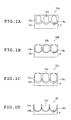
- FIGS. 1A to 1D are end views schematically showing an aluminum member and a microstructure for illustrating the inventive method of manufacturing microstructures.
- an aluminum member 10a includes an aluminum substrate 12a and an anodized film 14a which is present on a surface of the aluminum substrate 12a and has micropores 16a.
- the anodized film 14a has a barrier layer 18a on the side adjacent to the aluminum substrate 12a.
- the aluminum substrate is not subject to any particular limitation.
- Illustrative examples include pure aluminum plate; alloy plates composed primarily of aluminum and containing trace amounts of other elements; substrates made of low-purity aluminum (e.g., recycled material) on which high-purity aluminum has been vapor-deposited; substrates such as silicon wafers, quartz or glass whose surface has been covered with high-purity aluminum by a process such as vapor deposition or sputtering; and resin substrates on which aluminum has been laminated.
- the surface on which an anodized film is provided by anodizing treatment has an aluminum purity of preferably at least 99.5 wt%, more preferably at least 99.9 wt% and even more preferably at least 99.99 wt%.
- the pore arrangement will be sufficiently well-ordered.
- the aluminum substrate may be, for example, in the form of a web or discrete sheets.
- the pore-ordering treatment including the first film dissolution treatment and the anodizing treatment as well as the second film dissolution treatment, which will be described later, are preferably performed on the aluminum web as it is transported.
- transport rolls used for transporting the aluminum web each preferably has a radius of curvature of at least 50 mm, more preferably at least 70 mm and even more preferably at least 100 mm. At a radius of curvature within such range, the aluminum web is not strongly pressed against the transport rolls and is hence unlikely to tear.
- the aluminum web preferably has a width of at least 50 mm, more preferably at least 100 mm and even more preferably at least 150 mm. At a width within such range, the tension is unlikely to cause the aluminum web to tear.
- the aluminum web may be transported in a continuous or discontinuous manner.
- the surface of the aluminum substrate prefferably to be subjected beforehand to degreasing and mirror-like finishing treatment.
- microstructure obtained by the invention is to be used in applications that make use of its optical transparency, it is preferable that an aluminum substrate be subjected to heat treatment beforehand. Heat treatment will enlarge the region where the array of pores is highly ordered.
- the method of cooling is exemplified by a method involving direct immersion of the aluminum substrate in water or the like.
- degreasers may be used in degreasing treatment.
- degreasing may be carried out using any of various commercially available degreasers by the prescribed method.
- Preferred methods include the following: a method in which an organic solvent such as an alcohol (e.g., methanol), a ketone, benzine or a volatile oil is brought into contact with the aluminum surface at ambient temperature (organic solvent method); a method in which a liquid containing a surfactant such as soap or a neutral detergent is brought into contact with the aluminum surface at a temperature of from ambient temperature to 80°C, after which the surface is rinsed with water (surfactant method); a method in which an aqueous sulfuric acid solution having a concentration of 10 to 200 g/L is brought into contact with the aluminum surface at a temperature of from ambient temperature to 70°C for a period of 30 to 80 seconds, following which the surface is rinsed with water; a method in which an aqueous solution of sodium hydroxide having a concentration of 5 to 20 g/L is brought into contact with the aluminum surface at ambient temperature for about 30 seconds while electrolysis is carried out by passing a direct current through the aluminum surface as the cathode at a current
- the method used for degreasing is preferably one which can remove grease from the aluminum surface but causes substantially no aluminum dissolution.
- an organic solvent method, surfactant method, emulsion degreasing method or phosphate method is preferred.
- Mirror-like finishing treatment is carried out to eliminate surface asperities on the aluminum substrate and improve the uniformity and reproducibility of grain-forming treatment by a process such as electrodeposition.
- Examples of surface asperities on the aluminum member include rolling streaks formed during rolling when the aluminum member has been produced by a process including rolling.
- mirror-like finishing treatment is not subject to any particular limitation, and may be carried out using any suitable method known in the art. Examples of suitable methods include mechanical polishing, chemical polishing, and electrolytic polishing.
- Examples of chemical polishing methods include various methods mentioned in the 6th edition of Aluminum Handbook (Japan Aluminum Association, 2001), pp. 164-165 .
- Preferred examples include phosphoric acid/nitric acid method, Alupol I method, Alupol V method, Alcoa R5 method, H 3 PO 4 -CH 3 COOH-Cu method and H 3 PO 4 -HNO 3 -CH 3 COOH method.
- the phosphoric acid/nitric acid method, the H 3 PO 4 -CH 3 COOH-Cu method and the H 3 PO 4 -HNO 3 -CH 3 COOH method are especially preferred.
- electrolytic polishing methods include various methods mentioned in the 6th edition of Aluminum Handbook (Japan Aluminum Association, 2001), pp. 164-165 .
- a glossiness of at least 70% (in the case of rolled aluminum, at least 70% in both the rolling direction and the transverse direction) can be achieved.
- a method that uses an abrasive is carried out by changing over time the abrasive used from one having coarser particles to one having finer particles, following which electrolytic polishing is carried out.
- Mirror-like finishing treatment enables a surface having, for example, a mean surface roughness R a of 0.1 ⁇ m or less and a glossiness of at least 50% to be obtained.
- the mean surface roughness R a is preferably 0.03 ⁇ m or less, and more preferably 0.02 ⁇ m or less.
- the glossiness is preferably at least 70%, and more preferably at least 80%.
- the glossiness is the specular reflectance which can be determined in accordance with JIS Z8741-1997 (Method 3: 60° Specular Gloss) in a direction perpendicular to the rolling direction. Specifically, measurement is carried out using a variable-angle glossmeter (e.g., VG-1D, manufactured by Nippon Denshoku Industries Co., Ltd.) at an angle of incidence/reflection of 60° when the specular reflectance is 70% or less, and at an angle of incidence/reflection of 20° when the specular reflectance is more than 70%.
- VG-1D variable-angle glossmeter
- Any conventionally known method can be used for anodizing treatment. More specifically, a self-ordering method to be described below is preferably used.
- the self-ordering method is a method which enhances the orderliness by using the regularly arranging nature of micropores in the anodized film and eliminating factors that may disturb an orderly arrangement.
- an anodized film is formed on high-purity aluminum at a voltage appropriate for the type of electrolytic solution and at a low speed over an extended period of time (e.g., from several hours to well over ten hours).
- the desired pore diameter can be obtained to a certain degree by controlling the voltage.
- the average flow rate in anodizing treatment is preferably 0.5 to 20.0 m/min, more preferably 1.0 to 15.0 m/min and even more preferably 2.0 to 10.0 m/min. Uniformity and high orderliness can be achieved by performing anodizing treatment at a flow rate within the above range.
- the method of flowing the electrolytic solution under the condition described above is not subject to any particular limitation, and a method which uses a general stirring device such as a stirrer may be employed.
- a stirrer capable of controlling the stirring speed in the digital display mode is preferable because the average flow rate can be controlled.
- An example of such stirring device includes a magnetic stirrer HS-50D (produced by As One Corporation).
- Anodizing treatment may be carried out by, for example, a method that involves passing an electrical current through the aluminum substrate as the anode in a solution having an acid concentration of 1 to 10 wt%.
- Solutions that may be used in anodizing treatment are preferably acid solutions. It is preferable to use sulfuric acid, phosphoric acid, chromic acid, oxalic acid, sulfamic acid, benzenesulfonic acid and amidosulfonic acid, and more preferably sulfuric acid, phosphoric acid and oxalic acid. These acids may be used singly or in combination of two or more.
- the conditions for anodizing treatment vary depending on the electrolytic solution used, and thus cannot be strictly specified. However, it is generally preferable for the electrolyte concentration to be 0.1 to 20 wt%, the temperature of the solution to be -10 to 30°C, the current density to be 0.01 to 20 A/dm 2 , the voltage to be 3 to 300 V, and the period of electrolysis to be 0.5 to 30 hours. It is more preferable for the electrolyte concentration to be 0.5 to 15 wt%, the temperature of the solution to be -5 to 25°C, the current density to be 0.05 to 15 A/dm 2 , the voltage to be 5 to 250 V, and the period of electrolysis to be 1 to 25 hours.
- the anodized film has a dense barrier layer on the side adjacent to the aluminum substrate.
- the thickness of the barrier layer as used herein refers to a distance from the interface between the barrier layer and the aluminum substrate to the surface on the micropore side in the bottom of the micropore.
- the thickness of the barrier layer can be measured, for example, by observing a fracture surface of the aluminum member with an FE-SEM (field emission scanning electron microscope).
- anodizing treatment is performed at a constant voltage
- another method which involves changing the voltage continuously or intermittently may be used in anodizing treatment. In the latter case, it is preferable to gradually reduce the voltage. This method enables reduction of the resistance in the anodized film, thus achieving uniformity in the case where electrodeposition is to be performed later.
- the average pore density is preferably from 50 to 1,500 pores/ ⁇ m 2 .
- the area ratio occupied by the micropores is preferably from 20 to 50%.
- the area ratio occupied by the micropores is defined as the proportion of the sum of the areas of the individual micropore openings to the area of the aluminum surface.
- the method of calculating the degree of ordering of the micropores in the aluminum member is the same as that for the micropores in the microstructure to be described later except that the degree of ordering at the interface between the anodized film and the aluminum substrate is to be determined.
- This degree of ordering can be calculated after the bottoms of the micropores are bared by, for example, dissolving most of the anodized film in a mixed aqueous solution of phosphoric acid and chromic acid.
- Pore-ordering treatment is a treatment which involves performing one or more cycles of a step that includes a first film dissolution treatment for dissolving the anodized film until the thickness of the barrier layer is reduced to 3 to 50 nm and its subsequent anodizing treatment.
- the first film dissolution treatment is a treatment in which the anodized film in the aluminum member is dissolved until the thickness of the barrier layer is reduced to 3 to 50 nm.
- the first film dissolution treatment dissolves part of the anodized film surface with irregular pore-arrangement and therefore enhances the orderliness of the array of micropores.
- part of the interior of each micropore in the anodized film is also dissolved, but presence of the barrier layer with the thickness as defined above enables the anodized film to keep having starting points for anodizing treatment to be described later.
- the first film dissolution treatment causes the surface of the anodized film 14a and the interiors of the micropores 16a (i.e., the barrier layer 18a) shown in FIG. 1A to dissolve to thereby obtain an aluminum member 10b having on the aluminum substrate 12a an anodized film 14b bearing micropores 16b.
- the barrier layer 18a remains at the bottoms of the micropores 16b as a barrier layer 18b with a thickness of 3 to 50 nm.
- the first film dissolution treatment is carried out by bringing the aluminum member into contact with an aqueous acid solution or aqueous alkali solution.
- the contacting method is not particularly limited and is exemplified by immersion and spraying. Of these, immersion is preferable.
- the first film dissolution treatment is to be carried out with an aqueous alkali solution
- an aqueous solution of at least one alkali selected from the group consisting of sodium hydroxide, potassium hydroxide and lithium hydroxide it is preferable to use an aqueous solution of at least one alkali selected from the group consisting of sodium hydroxide, potassium hydroxide and lithium hydroxide. It is preferable for the aqueous alkali solution to have a concentration of 0.1 to 5 wt% and a temperature of 20 to 35°C.
- the aluminum member is immersed in the aqueous acid solution or aqueous alkali solution for a period of preferably 8 to 120 minutes, more preferably 10 to 90 minutes, and even more preferably 15 to 60 minutes.
- the anodized film is dissolved in the first film dissolution treatment to such an amount that the barrier layer after the dissolution of the anodized film may have a thickness of 3 to 50 nm, preferably 5 to 40 nm and more preferably 10 to 30 nm.
- the anodized film surface with irregular pore-arrangement is dissolved to enhance the orderliness of the array of micropores, while at the same time the anodized film at the bottoms of the micropores remain undissolved to keep having starting points for anodizing treatment to be described later.
- the first film dissolution treatment is followed by anodizing treatment, which causes the oxidation of the aluminum substrate to proceed to increase the thickness of the barrier layer of the anodized film that was partially dissolved in the first film dissolution treatment.
- anodizing treatment causes the oxidation of the aluminum substrate 12a shown in FIG. 1B to proceed to obtain an aluminum member 10c that has on an aluminum substrate 12b deeper micropores 16c than the micropores 16b and a thicker barrier layer 18c of an anodized film 14c than the barrier layer 18b of the anodized film 14b.
- Anodizing treatment may be carried out using a method known in the art, although it is preferably carried out under the same conditions as the above-described self-ordering method.
- Suitable use can also be made of a method in which the current is repeatedly turned on and off in an intermittent manner while keeping the dc voltage constant, and a method in which the current is repeatedly turned on and off while intermittently changing the dc voltage. Because these methods enables formation of micropores in the anodized film, they are preferable for improving uniformity, particularly when supporting the catalyst is carried out by electrodeposition.
- the thickness of the anodized film is preferably increased by 0. 1 to 100 ⁇ m and more preferably 0.5 to 50 ⁇ m. Within the above range, the orderliness of the array of pores can be more enhanced.
- pore-ordering treatment one or more cycles of the step that includes the first film dissolution treatment and its subsequent anodizing treatment as described above are performed.
- this step is repeatedly performed preferably twice or more, more preferably three times or more, and even more preferably four times or more.
- the conditions of the first film dissolution treatment steps and the anodizing treatment steps in the respective cycles may be the same or different.
- different voltages may be used in two or more anodizing treatment steps from the viewpoint of enhancing the degree of ordering. In this case, it is more preferable to perform pore-ordering treatment under the conditions of gradually increased voltages from the viewpoint of enhancing the degree of ordering.
- the second film dissolution treatment may be basically performed on the same conditions as those in the first film dissolution treatment, so differences are only described below.
- the amount of material dissolved out of the anodized film in the second film dissolution treatment is not particularly limited and is preferably 0.01 to 30 wt% and more preferably 0.1 to 15 wt%.
- the manufacturing method of the invention yields the microstructure of the invention.
- the average pore density of the microstructure of the invention is preferably from 50 to 1,500 pores/ ⁇ m 2 .
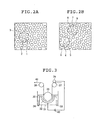
- micropore 1 shown in FIG. 2A
- a circle 3 is drawn so as to be centered on the center of gravity of the micropore 1 and so as to be of the smallest radius that is internally tangent to the edge of another micropore (inscribed in a micropore 2)
- the interior of the circle 3 includes the centers of gravity of six micropores other than the micropore 1. Therefore, the micropore 1 is counted for B.
- micropore 4 shown in FIG. 2B
- a circle 6 is drawn so as to be centered on the center of gravity of the micropore 4 and so as to be of the smallest radius that is internally tangent to the edge of another micropore (inscribed in a micropore 5)
- the interior of the circle 6 includes the centers of gravity of five micropores other than the micropore 4. Therefore, the micropore 4 is not counted for B.
- hydrophilizing treatment may be performed to reduce the contact angle with water.
- Such hydrophilizing treatment may be performed by a method known in the art.
- the aluminum substrate may be removed depending on the intended application.
- the method of removing the aluminum substrate is not subject to any particular limitation, and it is preferable to use, for example, a method in which the aluminum substrate is immersed in a solvent in which alumina is hardly soluble or insoluble but aluminum is soluble.
- Preferred solvents that may be used include halogen solvents (e.g., bromine and iodine); acidic solvents such as dilute sulfuric acid, phosphoric acid, oxalic acid, sulfamic acid, benzenesulfonic acid and amidosulfonic acid; and alkaline solvents such as sodium hydroxide, potassium hydroxide and calcium hydroxide. Bromine and iodine are particularly preferable.
- halogen solvents e.g., bromine and iodine
- acidic solvents such as dilute sulfuric acid, phosphoric acid, oxalic acid, sulfamic acid, benzenesulfonic acid and amidosulfonic acid
- alkaline solvents such as sodium hydroxide, potassium hydroxide and calcium hydroxide. Bromine and iodine are particularly preferable.
- the microstructure of the invention may support a catalyst in the micropores of the anodized film according to the intended application.
- the catalyst is not subject to any particular limitation as long as the catalyst used has a catalytic function, and examples of the catalyst that may be used include AlCl 3 , AlBr 3 , Al 2 O 3 , SiO 2 , SiO 2 -Al 2 O 2 , silicon zeolite, SiO 2 -NiO active carbon, PbO/Al 2 O 3 , LaCoO 3 H 3 PO 4 , H 4 P 2 O 7 , Bi 2 O 3 -MoO 3 , Sb 2 O 5 , SbO 2 -Fe 2 O 3 , SnO 2 -Sb 2 O 5 , Cu, CuO 2 -Cr 2 O 3 , Cu-Cr 2 O 3 -ZnO, Cu/SiO 2 , CuCl 2 , Ag/ ⁇ -Al 2 O 3 , Au, ZnO, ZnO-Cr 2 O 3 , ZnCl 2 , ZnO-Al 2 O 3 -CaO, TiO 2
- the method of supporting the catalyst is not particularly limited but any conventionally known technique may be used.
- Examples of preferred techniques include electrodeposition, and a method which involves coating the aluminum member having the anodized film with a dispersion of catalyst particles, then drying.
- the catalyst is preferably in the form of single particles or agglomerates.
- An electrodeposition method known in the art may be used.
- use may be made of a process in which the aluminum member is immersed in a 30°C dispersion containing 1 g/L of HAuCl 4 and 7 g/L of H 2 SO 4 and electrodeposition is carried out at a constant voltage of 11 V (regulated with an autotransformer such as SLIDAC) for 5 to 6 minutes.
- an autotransformer such as SLIDAC
- the dispersions employed in methods which use catalyst particles can be obtained by a conventionally known method.
- Illustrative examples include methods of preparing fine particles by low-vacuum vapor deposition and methods of preparing catalyst colloids by reducing an aqueous solution of a catalyst salt.
- the colloidal catalyst particles have an average particle size of preferably 1 to 200 nm, more preferably 1 to 100 nm, and even more preferably 2 to 80 nm.
- Preferred use can be made of water as the dispersion medium employed in the dispersion.
- Use can also be made of a mixed solvent composed of water and a solvent that is miscible with water, such as an alcohol, illustrative examples of which include ethyl alcohol, n-propyl alcohol, i-propyl alcohol, 1-butyl alcohol, 2-butyl alcohol, t-butyl alcohol, methyl cellosolve and butyl cellosolve.
- dispersions that may be employed in methods which use colloidal catalyst particles include dispersions of colloidal gold particles and dispersions of colloidal silver particles.
- Dispersions of colloidal gold particles that may be used include those described in JP 2001-89140 A and JP 11-80647 A . Commercial products may also be used.
- Dispersions of colloidal silver particles preferably contain particles of silver-palladium alloys because these are not affected by the acids which leach out of the anodized film.
- the palladium content in such a case is preferably from 5 to 30 wt%.
- the surface porosity after catalyst supporting treatment is preferably not more than 70%, more preferably not more than 50% and even more preferably not more than 30%.
- the surface porosity after catalyst supporting treatment is defined as the sum of the areas of the openings in micropores having no catalyst supported therein relative to the area of the aluminum surface.
- Colloidal catalyst particles which may be used in the dispersion generally have a dispersion in the particle size distribution, expressed as the coefficient of variation, of about 10 to 20%.
- a dispersion in the particle size distribution expressed as the coefficient of variation, of about 10 to 20%.
- suitable use may be made of a method which employs colloidal catalyst particles.
- suitable use may be made of an electrodeposition process.
- Suitable use may also be made of a method which combines both approaches.
- microstructure of the invention has regularly arranged micropores, and can therefore be employed in various applications.
- substrate samples were subjected to the following treatments as shown in Tables 1-1 to 1-3: The substrate samples were subjected to preanodizing treatment, which was followed by pore-ordering treatment in Examples 1 to 6 and Comparative Examples 2 and 3 or film removal treatment and its subsequent anodizing treatment in Comparative Example 1; the second film dissolution treatment was then performed to yield microstructures.
- a dash (-) indicates that the treatment in question was not carried out.
- polishing with an abrasive cloth, buffing, then electrolytic polishing were carried out in this order. After buffing, the substrate was rinsed with water.
- Polishing with an abrasive cloth was carried out using a polishing platen (Abramin, produced by Marumoto Struers K.K.) and commercial water-resistant abrasive cloths. This polishing operation was carried out while successively changing the grit size of the water-resistant abrasive cloths in the following order: #200, #500, #800, #1000 and #1500.
- FM No. 3 average particle size, 1 ⁇ m
- FM No. 4 average particle size, 0.3 ⁇ m
- Electrolytic polishing was carried out for 2 minutes in an electrolytic solution of the composition indicated below (temperature, 70°C), using the substrate as the anode and a carbon electrode as the cathode, and at a constant current of 130 mA/cm 2 .
- the power supply was a GP0110-30R unit manufactured by Takasago, Ltd.
- Preanodizing treatment was performed under the conditions shown in Table 1-1 or 1-2 on the surface of each substrate which had been mirror-like finished.
- the substrate immersed in the electrolytic solution was subjected to self-ordering anodizing treatment according to such conditions as the type and concentration of the electrolytic solution, voltage, temperature, average flow rate and treatment time shown in Table 1-1 or 1-2, thereby forming an anodized film having a thickness of about 12 ⁇ m.
- the barrier layer of the anodized film had a thickness of about 50 nm.
- NeoCool BD36 (Yamato Scientific Co., Ltd.) as the cooling system
- Pairstirrer PS-100 (Tokyo Rikakikai Co., Ltd.)
- GP0650-2R unit Teakasago, Ltd.
- the average flow rate of the electrolytic solution was measured using the vortex flow monitor FLM22-10PCW (manufactured by As One Corporation).
- the anodized film thickness was measured using the eddy current thickness gauge EDY-1000 (manufactured by Sanko Electronic Laboratory Co., Ltd.).
- the thickness of the barrier layer was measured by observing the fracture surface of the aluminum member with the FE-SEM.
- the degree of ordering of micropores at the interface between the anodized film and the aluminum substrate in the aluminum member was also measured. More specifically, the aluminum member was immersed in an aqueous solution of chromic anhydride and phosphoric acid as defined in JIS H8688 (1998)-H8688 at 50°C for 12 hours. Then, its surface was photographed with the FE-SEM (at a magnification of 20,000X) and the degree of micropore ordering as defined by formula (1) was measured with a field of view of 2 ⁇ m x 2 ⁇ m. The degree of ordering was measured at 10 points and the average of the measurements obtained was calculated. The results are shown in Table 1-4.
- the aluminum member having the anodized film was immersed in the treatment solution of the type, concentration and temperature shown in Table 1-2 for the period shown in Table 1-2.
- the anodized film thickness was measured by the same method as above.
- pore-ordering treatment was performed which involved performing one or more cycles of a step that included a first film dissolution treatment for dissolving part of the anodized film having undergone preanodizing treatment and its subsequent anodizing treatment.
- each aluminum member was immersed in the treatment solution of the type, concentration and temperature shown in any of Tables 1-1 to 1-3 for the period shown in any of Tables 1-1 to 1-3 to perform the first film dissolution treatment.
- the barrier layer thickness was measured by the same method as above. The results are shown in Table 1-4.
- Anodizing treatment enabled the barrier layer of the anodized film in each aluminum member to grow to a thickness of about 50 nm.
- a substrate which was an aluminum web, was subjected to mirror-like finishing treatment through electrolytic polishing, preanodizing treatment, pore-ordering treatment and second film dissolution treatment in this order to yield a microstructure.
- the substrate was subjected to electrolytic polishing for mirror-like finishing treatment.
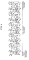
- FIG. 3 shows an electrolytic cell 31, a cathode electrode 32, an electrolytic solution inlet 33, an electrolytic solution outlet 34, an electrolytic solution 35, a drum roller 36, transport rollers 37, 38, a conductor roll 39, a power supply 40 and a substrate 41.
- the first anodizing treatment step corresponds to preanodizing treatment
- the fifth film dissolution treatment step to the second film dissolution treatment
- the four film dissolution treatment steps and four anodizing treatment steps which were performed between the first anodizing treatment step and the fifth film dissolution treatment step correspond to pore-ordering treatment.
- FIG. 4 shows electrolytic cells 42, cathode electrodes 43, electrolytic solution inlets 44, electrolytic solution outlets 45, an electrolytic solution 46, drum rollers 47, transport rollers 48, 49, conductor rolls 50, power supplies 51, film dissolution treatment tanks 52, guide plates 53 for a film dissolution treatment solution, film dissolution treatment solution inlets 54, film dissolution treatment solution outlets 55, the film dissolution treatment solution 56, drum rollers 57, transport rollers 58, 59, water rinsing sections 60, air drying sections 61 and a substrate 62.
- the substrate was immersed in an electrolytic solution (an aqueous solution of 0.3 mol/L sulfuric acid (Wako Pure Chemical Industries, Ltd.); temperature, 15 °C) to perform electrolysis under the conditions of a voltage of 25V, an electrolytic solution average flow rate of 0.3 m/min, a substrate transport rate of 50 mm/min, and a treatment time of 60 minutes, whereby an anodized film was formed.
- the electrolytic solution flowed in the same direction as the direction of transport of the substrate (see FIG. 4).
- the anodized film had a thickness of about 12 ⁇ m and the barrier layer of the anodized film had a thickness of about 50 nm.
- the thickness of the anodized film and that of the barrier layer were measured by the same method as used in Examples 1 to 6 and Comparative Examples 1 to 3.
- the five film dissolution treatment steps were performed by immersing the anodized substrate in a treatment solution for film dissolution (aqueous solution of 0.6 mol/L phosphoric acid (Wako Pure Chemical Industries, Ltd.); temperature, 40 °C) under the condition of a treatment solution average flow rate of 2 m/min.
- a treatment solution for film dissolution aqueous solution of 0.6 mol/L phosphoric acid (Wako Pure Chemical Industries, Ltd.); temperature, 40 °C) under the condition of a treatment solution average flow rate of 2 m/min.
- the treatment solution for film dissolution flowed in the same direction as the direction of transport of the substrate (see FIG. 4).
- the thickness of the barrier layer was measured by the same method as above after each of the first to fourth film dissolution treatment steps was performed. As a result, a barrier layer thickness of 10 nm was obtained after each of the first to fourth film dissolution treatment steps.
- the ratio "a/b" of the diameter of a micropore opening "a” to the micropore diameter at the height "a/2" from the micropore bottom "b” was measured by the same method as used in Examples 1 to 6 and Comparative Examples 1 to 3. As a result, the ratio "a/b" was 0.98.
- the inventive method of manufacturing microstructures does not require film removal treatment with a mixed aqueous solution of phosphoric acid and chromic acid and can therefore provide microstructures having highly ordered arrays of pores in a short period of time compared with the case where film removal treatment is performed (as in Comparative Example 1).
- Table 1-1 Example 1
- Example 2 Example 3
- Example 4 Example 5
- Example 6 Example 6
Landscapes
- Chemical & Material Sciences (AREA)
- Engineering & Computer Science (AREA)
- Chemical Kinetics & Catalysis (AREA)
- Electrochemistry (AREA)
- Materials Engineering (AREA)
- Metallurgy (AREA)
- Organic Chemistry (AREA)
- Other Surface Treatments For Metallic Materials (AREA)
- ing And Chemical Polishing (AREA)
- Materials For Photolithography (AREA)
- Manufacturing Of Magnetic Record Carriers (AREA)
Applications Claiming Priority (1)
| Application Number | Priority Date | Filing Date | Title |
|---|---|---|---|
| JP2006167540A JP4800860B2 (ja) | 2006-06-16 | 2006-06-16 | 微細構造体の製造方法および微細構造体 |
Publications (2)
| Publication Number | Publication Date |
|---|---|
| EP1867757A2 true EP1867757A2 (fr) | 2007-12-19 |
| EP1867757A3 EP1867757A3 (fr) | 2011-04-13 |
Family
ID=38595967
Family Applications (1)
| Application Number | Title | Priority Date | Filing Date |
|---|---|---|---|
| EP20070011664 Withdrawn EP1867757A3 (fr) | 2006-06-16 | 2007-06-14 | Microstructure et son procédé de fabrication |
Country Status (3)
| Country | Link |
|---|---|
| US (1) | US7722754B2 (fr) |
| EP (1) | EP1867757A3 (fr) |
| JP (1) | JP4800860B2 (fr) |
Cited By (3)
| Publication number | Priority date | Publication date | Assignee | Title |
|---|---|---|---|---|
| US20130171289A1 (en) * | 2011-12-29 | 2013-07-04 | Chia-Ling Hsu | Roller and method of making roller |
| EP2400597A4 (fr) * | 2009-02-17 | 2014-07-02 | Fujifilm Corp | Élément anisotropiquement conducteur et son procédé de fabrication |
| CN110656366A (zh) * | 2018-06-29 | 2020-01-07 | 深圳市裕展精密科技有限公司 | 铝合金的阳极氧化方法 |
Families Citing this family (6)
| Publication number | Priority date | Publication date | Assignee | Title |
|---|---|---|---|---|
| CN101971037A (zh) | 2008-03-14 | 2011-02-09 | 富士胶片株式会社 | 探针卡 |
| JP5155704B2 (ja) * | 2008-03-18 | 2013-03-06 | 財団法人神奈川科学技術アカデミー | 表面に微細構造を有するアルミニウムの製造方法およびポーラスアルミナの製造方法 |
| KR101332422B1 (ko) * | 2011-01-07 | 2013-12-02 | 건국대학교 산학협력단 | 전기화학성장을 이용한 단결정 산화구리 (i) 나노선 어레이 제조 방법 |
| JPWO2012176794A1 (ja) * | 2011-06-22 | 2015-02-23 | 三菱レイヨン株式会社 | ロール状金型の製造方法、および微細凹凸構造を表面に有する物品の製造方法 |
| JP5536287B1 (ja) * | 2012-08-06 | 2014-07-02 | 三菱レイヨン株式会社 | モールドの製造方法、および微細凹凸構造を表面に有する成形体の製造方法 |
| EP3428955A1 (fr) * | 2017-07-10 | 2019-01-16 | Murata Manufacturing Co., Ltd. | Substrats faisant appel à l'amplification de superficie à utiliser dans la fabrication d'éléments capacitifs et d'autres dispositifs |
Family Cites Families (14)
| Publication number | Priority date | Publication date | Assignee | Title |
|---|---|---|---|---|
| AR208421A1 (es) * | 1975-07-16 | 1976-12-27 | Alcan Res & Dev | Articulo de aluminio electroliticamente anodizado y coloreado y un metodo para producir el mismo |
| US20020145826A1 (en) * | 2001-04-09 | 2002-10-10 | University Of Alabama | Method for the preparation of nanometer scale particle arrays and the particle arrays prepared thereby |
| JP2004217961A (ja) | 2003-01-10 | 2004-08-05 | Kanagawa Acad Of Sci & Technol | 陽極酸化ポーラスアルミナ複合体及びその製造方法 |
| JP4222861B2 (ja) * | 2003-03-20 | 2009-02-12 | 財団法人神奈川科学技術アカデミー | 陽極酸化ポーラスアルミナおよびその製造方法 |
| JP4406553B2 (ja) * | 2003-11-21 | 2010-01-27 | 財団法人神奈川科学技術アカデミー | 反射防止膜の製造方法 |
| JP4631047B2 (ja) * | 2004-01-05 | 2011-02-16 | 国立大学法人広島大学 | 陽極酸化アルミナ膜を具備する構造体およびその製造方法並びにその利用 |
| JP4445766B2 (ja) * | 2004-02-10 | 2010-04-07 | 財団法人神奈川科学技術アカデミー | 陽極酸化ポーラスアルミナの製造方法 |
| JP2005307341A (ja) | 2004-03-23 | 2005-11-04 | Fuji Photo Film Co Ltd | 微細構造体およびその製造方法 |
| EP1580305A3 (fr) * | 2004-03-23 | 2008-01-16 | FUJIFILM Corporation | Surface structurelle d'un corps et méthode pour sa production |
| US20070235342A1 (en) * | 2004-10-01 | 2007-10-11 | Canon Kabushiki Kaisha | Method for manufacturing nanostructure |
| JP2006124827A (ja) * | 2004-10-01 | 2006-05-18 | Canon Inc | ナノ構造体の製造方法 |
| JP4813925B2 (ja) * | 2006-02-28 | 2011-11-09 | 富士フイルム株式会社 | 微細構造体の製造方法および微細構造体 |
| JP2007238988A (ja) * | 2006-03-07 | 2007-09-20 | Fujifilm Corp | 微細構造体の製造方法および微細構造体 |
| JP4768478B2 (ja) * | 2006-03-17 | 2011-09-07 | 富士フイルム株式会社 | 微細構造体の製造方法および微細構造体 |
-
2006
- 2006-06-16 JP JP2006167540A patent/JP4800860B2/ja active Active
-
2007
- 2007-06-11 US US11/808,502 patent/US7722754B2/en not_active Expired - Fee Related
- 2007-06-14 EP EP20070011664 patent/EP1867757A3/fr not_active Withdrawn
Cited By (4)
| Publication number | Priority date | Publication date | Assignee | Title |
|---|---|---|---|---|
| EP2400597A4 (fr) * | 2009-02-17 | 2014-07-02 | Fujifilm Corp | Élément anisotropiquement conducteur et son procédé de fabrication |
| US20130171289A1 (en) * | 2011-12-29 | 2013-07-04 | Chia-Ling Hsu | Roller and method of making roller |
| US8881402B2 (en) * | 2011-12-29 | 2014-11-11 | Hon Hai Precision Industry Co., Ltd. | Roller and method of making roller |
| CN110656366A (zh) * | 2018-06-29 | 2020-01-07 | 深圳市裕展精密科技有限公司 | 铝合金的阳极氧化方法 |
Also Published As
| Publication number | Publication date |
|---|---|
| EP1867757A3 (fr) | 2011-04-13 |
| JP2007332437A (ja) | 2007-12-27 |
| JP4800860B2 (ja) | 2011-10-26 |
| US7722754B2 (en) | 2010-05-25 |
| US20070289945A1 (en) | 2007-12-20 |
Similar Documents
| Publication | Publication Date | Title |
|---|---|---|
| US7699971B2 (en) | Microstructure and method of manufacturing the same | |
| EP1826298B1 (fr) | Microstructure et son procédé de fabrication | |
| US7824535B2 (en) | Microstructure and method of manufacturing the same | |
| US7722754B2 (en) | Microstructure and method of manufacturing the same | |
| EP2399694A1 (fr) | Élément métallique | |
| EP2213771B1 (fr) | Structure microfine | |
| US20080029399A1 (en) | Method of manufacturing nanostructures | |
| JP4800799B2 (ja) | 微細構造体の製造方法および微細構造体 | |
| EP2270262A1 (fr) | Microstructure et son procédé de fabrication | |
| JP4768478B2 (ja) | 微細構造体の製造方法および微細構造体 | |
| JP2007238988A (ja) | 微細構造体の製造方法および微細構造体 | |
| JP2007204802A (ja) | 構造体の製造方法 | |
| JP4884202B2 (ja) | 微細構造体の製造方法および微細構造体 | |
| JP2007211306A (ja) | ナノ構造体の製造方法 | |
| WO2011034008A1 (fr) | Microstructure et son procédé de production | |
| JP2008063643A (ja) | 微細構造体の製造方法および微細構造体 | |
| JP2010168617A (ja) | 微細構造体の製造方法 | |
| JP2008057018A (ja) | 微細構造体の製造方法および微細構造体 |
Legal Events
| Date | Code | Title | Description |
|---|---|---|---|
| PUAI | Public reference made under article 153(3) epc to a published international application that has entered the european phase |
Free format text: ORIGINAL CODE: 0009012 |
|
| AK | Designated contracting states |
Kind code of ref document: A2 Designated state(s): AT BE BG CH CY CZ DE DK EE ES FI FR GB GR HU IE IS IT LI LT LU LV MC MT NL PL PT RO SE SI SK TR |
|
| AX | Request for extension of the european patent |
Extension state: AL BA HR MK YU |
|
| PUAL | Search report despatched |
Free format text: ORIGINAL CODE: 0009013 |
|
| AK | Designated contracting states |
Kind code of ref document: A3 Designated state(s): AT BE BG CH CY CZ DE DK EE ES FI FR GB GR HU IE IS IT LI LT LU LV MC MT NL PL PT RO SE SI SK TR |
|
| AX | Request for extension of the european patent |
Extension state: AL BA HR MK RS |
|
| RIC1 | Information provided on ipc code assigned before grant |
Ipc: C25D 11/18 20060101ALI20110307BHEP Ipc: C25D 11/12 20060101ALI20110307BHEP Ipc: C25D 11/04 20060101AFI20071024BHEP |
|
| AKY | No designation fees paid | ||
| REG | Reference to a national code |
Ref country code: DE Ref legal event code: R108 |
|
| REG | Reference to a national code |
Ref country code: DE Ref legal event code: R108 Effective date: 20111221 |
|
| STAA | Information on the status of an ep patent application or granted ep patent |
Free format text: STATUS: THE APPLICATION IS DEEMED TO BE WITHDRAWN |
|
| 18D | Application deemed to be withdrawn |
Effective date: 20111014 |