EP1870875A2 - Elektrooptische Vorrichtung, Verfahren zur Ansteuerung einer elektrooptischen Vorrichtung und elektronisches Gerät - Google Patents
Elektrooptische Vorrichtung, Verfahren zur Ansteuerung einer elektrooptischen Vorrichtung und elektronisches Gerät Download PDFInfo
- Publication number
- EP1870875A2 EP1870875A2 EP07075846A EP07075846A EP1870875A2 EP 1870875 A2 EP1870875 A2 EP 1870875A2 EP 07075846 A EP07075846 A EP 07075846A EP 07075846 A EP07075846 A EP 07075846A EP 1870875 A2 EP1870875 A2 EP 1870875A2
- Authority
- EP
- European Patent Office
- Prior art keywords
- data
- scanning
- pixel
- electro
- line
- Prior art date
- Legal status (The legal status is an assumption and is not a legal conclusion. Google has not performed a legal analysis and makes no representation as to the accuracy of the status listed.)
- Withdrawn
Links
Images






Classifications
-
- G—PHYSICS
- G09—EDUCATION; CRYPTOGRAPHY; DISPLAY; ADVERTISING; SEALS
- G09G—ARRANGEMENTS OR CIRCUITS FOR CONTROL OF INDICATING DEVICES USING STATIC MEANS TO PRESENT VARIABLE INFORMATION
- G09G3/00—Control arrangements or circuits, of interest only in connection with visual indicators other than cathode-ray tubes
- G09G3/20—Control arrangements or circuits, of interest only in connection with visual indicators other than cathode-ray tubes for presentation of an assembly of a number of characters, e.g. a page, by composing the assembly by combination of individual elements arranged in a matrix no fixed position being assigned to or needed to be assigned to the individual characters or partial characters
- G09G3/22—Control arrangements or circuits, of interest only in connection with visual indicators other than cathode-ray tubes for presentation of an assembly of a number of characters, e.g. a page, by composing the assembly by combination of individual elements arranged in a matrix no fixed position being assigned to or needed to be assigned to the individual characters or partial characters using controlled light sources
- G09G3/30—Control arrangements or circuits, of interest only in connection with visual indicators other than cathode-ray tubes for presentation of an assembly of a number of characters, e.g. a page, by composing the assembly by combination of individual elements arranged in a matrix no fixed position being assigned to or needed to be assigned to the individual characters or partial characters using controlled light sources using electroluminescent panels
-
- G—PHYSICS
- G09—EDUCATION; CRYPTOGRAPHY; DISPLAY; ADVERTISING; SEALS
- G09G—ARRANGEMENTS OR CIRCUITS FOR CONTROL OF INDICATING DEVICES USING STATIC MEANS TO PRESENT VARIABLE INFORMATION
- G09G3/00—Control arrangements or circuits, of interest only in connection with visual indicators other than cathode-ray tubes
- G09G3/20—Control arrangements or circuits, of interest only in connection with visual indicators other than cathode-ray tubes for presentation of an assembly of a number of characters, e.g. a page, by composing the assembly by combination of individual elements arranged in a matrix no fixed position being assigned to or needed to be assigned to the individual characters or partial characters
- G09G3/22—Control arrangements or circuits, of interest only in connection with visual indicators other than cathode-ray tubes for presentation of an assembly of a number of characters, e.g. a page, by composing the assembly by combination of individual elements arranged in a matrix no fixed position being assigned to or needed to be assigned to the individual characters or partial characters using controlled light sources
- G09G3/30—Control arrangements or circuits, of interest only in connection with visual indicators other than cathode-ray tubes for presentation of an assembly of a number of characters, e.g. a page, by composing the assembly by combination of individual elements arranged in a matrix no fixed position being assigned to or needed to be assigned to the individual characters or partial characters using controlled light sources using electroluminescent panels
- G09G3/32—Control arrangements or circuits, of interest only in connection with visual indicators other than cathode-ray tubes for presentation of an assembly of a number of characters, e.g. a page, by composing the assembly by combination of individual elements arranged in a matrix no fixed position being assigned to or needed to be assigned to the individual characters or partial characters using controlled light sources using electroluminescent panels semiconductive, e.g. using light-emitting diodes [LED]
- G09G3/3208—Control arrangements or circuits, of interest only in connection with visual indicators other than cathode-ray tubes for presentation of an assembly of a number of characters, e.g. a page, by composing the assembly by combination of individual elements arranged in a matrix no fixed position being assigned to or needed to be assigned to the individual characters or partial characters using controlled light sources using electroluminescent panels semiconductive, e.g. using light-emitting diodes [LED] organic, e.g. using organic light-emitting diodes [OLED]
- G09G3/3225—Control arrangements or circuits, of interest only in connection with visual indicators other than cathode-ray tubes for presentation of an assembly of a number of characters, e.g. a page, by composing the assembly by combination of individual elements arranged in a matrix no fixed position being assigned to or needed to be assigned to the individual characters or partial characters using controlled light sources using electroluminescent panels semiconductive, e.g. using light-emitting diodes [LED] organic, e.g. using organic light-emitting diodes [OLED] using an active matrix
- G09G3/3233—Control arrangements or circuits, of interest only in connection with visual indicators other than cathode-ray tubes for presentation of an assembly of a number of characters, e.g. a page, by composing the assembly by combination of individual elements arranged in a matrix no fixed position being assigned to or needed to be assigned to the individual characters or partial characters using controlled light sources using electroluminescent panels semiconductive, e.g. using light-emitting diodes [LED] organic, e.g. using organic light-emitting diodes [OLED] using an active matrix with pixel circuitry controlling the current through the light-emitting element
- G09G3/3241—Control arrangements or circuits, of interest only in connection with visual indicators other than cathode-ray tubes for presentation of an assembly of a number of characters, e.g. a page, by composing the assembly by combination of individual elements arranged in a matrix no fixed position being assigned to or needed to be assigned to the individual characters or partial characters using controlled light sources using electroluminescent panels semiconductive, e.g. using light-emitting diodes [LED] organic, e.g. using organic light-emitting diodes [OLED] using an active matrix with pixel circuitry controlling the current through the light-emitting element the current through the light-emitting element being set using a data current provided by the data driver, e.g. by using a two-transistor current mirror
-
- G—PHYSICS
- G09—EDUCATION; CRYPTOGRAPHY; DISPLAY; ADVERTISING; SEALS
- G09G—ARRANGEMENTS OR CIRCUITS FOR CONTROL OF INDICATING DEVICES USING STATIC MEANS TO PRESENT VARIABLE INFORMATION
- G09G3/00—Control arrangements or circuits, of interest only in connection with visual indicators other than cathode-ray tubes
- G09G3/20—Control arrangements or circuits, of interest only in connection with visual indicators other than cathode-ray tubes for presentation of an assembly of a number of characters, e.g. a page, by composing the assembly by combination of individual elements arranged in a matrix no fixed position being assigned to or needed to be assigned to the individual characters or partial characters
- G09G3/2007—Display of intermediate tones
- G09G3/2011—Display of intermediate tones by amplitude modulation
-
- G—PHYSICS
- G09—EDUCATION; CRYPTOGRAPHY; DISPLAY; ADVERTISING; SEALS
- G09G—ARRANGEMENTS OR CIRCUITS FOR CONTROL OF INDICATING DEVICES USING STATIC MEANS TO PRESENT VARIABLE INFORMATION
- G09G3/00—Control arrangements or circuits, of interest only in connection with visual indicators other than cathode-ray tubes
- G09G3/20—Control arrangements or circuits, of interest only in connection with visual indicators other than cathode-ray tubes for presentation of an assembly of a number of characters, e.g. a page, by composing the assembly by combination of individual elements arranged in a matrix no fixed position being assigned to or needed to be assigned to the individual characters or partial characters
- G09G3/22—Control arrangements or circuits, of interest only in connection with visual indicators other than cathode-ray tubes for presentation of an assembly of a number of characters, e.g. a page, by composing the assembly by combination of individual elements arranged in a matrix no fixed position being assigned to or needed to be assigned to the individual characters or partial characters using controlled light sources
- G09G3/30—Control arrangements or circuits, of interest only in connection with visual indicators other than cathode-ray tubes for presentation of an assembly of a number of characters, e.g. a page, by composing the assembly by combination of individual elements arranged in a matrix no fixed position being assigned to or needed to be assigned to the individual characters or partial characters using controlled light sources using electroluminescent panels
- G09G3/32—Control arrangements or circuits, of interest only in connection with visual indicators other than cathode-ray tubes for presentation of an assembly of a number of characters, e.g. a page, by composing the assembly by combination of individual elements arranged in a matrix no fixed position being assigned to or needed to be assigned to the individual characters or partial characters using controlled light sources using electroluminescent panels semiconductive, e.g. using light-emitting diodes [LED]
- G09G3/3208—Control arrangements or circuits, of interest only in connection with visual indicators other than cathode-ray tubes for presentation of an assembly of a number of characters, e.g. a page, by composing the assembly by combination of individual elements arranged in a matrix no fixed position being assigned to or needed to be assigned to the individual characters or partial characters using controlled light sources using electroluminescent panels semiconductive, e.g. using light-emitting diodes [LED] organic, e.g. using organic light-emitting diodes [OLED]
- G09G3/3225—Control arrangements or circuits, of interest only in connection with visual indicators other than cathode-ray tubes for presentation of an assembly of a number of characters, e.g. a page, by composing the assembly by combination of individual elements arranged in a matrix no fixed position being assigned to or needed to be assigned to the individual characters or partial characters using controlled light sources using electroluminescent panels semiconductive, e.g. using light-emitting diodes [LED] organic, e.g. using organic light-emitting diodes [OLED] using an active matrix
- G09G3/3233—Control arrangements or circuits, of interest only in connection with visual indicators other than cathode-ray tubes for presentation of an assembly of a number of characters, e.g. a page, by composing the assembly by combination of individual elements arranged in a matrix no fixed position being assigned to or needed to be assigned to the individual characters or partial characters using controlled light sources using electroluminescent panels semiconductive, e.g. using light-emitting diodes [LED] organic, e.g. using organic light-emitting diodes [OLED] using an active matrix with pixel circuitry controlling the current through the light-emitting element
-
- G—PHYSICS
- G09—EDUCATION; CRYPTOGRAPHY; DISPLAY; ADVERTISING; SEALS
- G09G—ARRANGEMENTS OR CIRCUITS FOR CONTROL OF INDICATING DEVICES USING STATIC MEANS TO PRESENT VARIABLE INFORMATION
- G09G3/00—Control arrangements or circuits, of interest only in connection with visual indicators other than cathode-ray tubes
- G09G3/20—Control arrangements or circuits, of interest only in connection with visual indicators other than cathode-ray tubes for presentation of an assembly of a number of characters, e.g. a page, by composing the assembly by combination of individual elements arranged in a matrix no fixed position being assigned to or needed to be assigned to the individual characters or partial characters
- G09G3/22—Control arrangements or circuits, of interest only in connection with visual indicators other than cathode-ray tubes for presentation of an assembly of a number of characters, e.g. a page, by composing the assembly by combination of individual elements arranged in a matrix no fixed position being assigned to or needed to be assigned to the individual characters or partial characters using controlled light sources
- G09G3/30—Control arrangements or circuits, of interest only in connection with visual indicators other than cathode-ray tubes for presentation of an assembly of a number of characters, e.g. a page, by composing the assembly by combination of individual elements arranged in a matrix no fixed position being assigned to or needed to be assigned to the individual characters or partial characters using controlled light sources using electroluminescent panels
- G09G3/32—Control arrangements or circuits, of interest only in connection with visual indicators other than cathode-ray tubes for presentation of an assembly of a number of characters, e.g. a page, by composing the assembly by combination of individual elements arranged in a matrix no fixed position being assigned to or needed to be assigned to the individual characters or partial characters using controlled light sources using electroluminescent panels semiconductive, e.g. using light-emitting diodes [LED]
- G09G3/3208—Control arrangements or circuits, of interest only in connection with visual indicators other than cathode-ray tubes for presentation of an assembly of a number of characters, e.g. a page, by composing the assembly by combination of individual elements arranged in a matrix no fixed position being assigned to or needed to be assigned to the individual characters or partial characters using controlled light sources using electroluminescent panels semiconductive, e.g. using light-emitting diodes [LED] organic, e.g. using organic light-emitting diodes [OLED]
- G09G3/3225—Control arrangements or circuits, of interest only in connection with visual indicators other than cathode-ray tubes for presentation of an assembly of a number of characters, e.g. a page, by composing the assembly by combination of individual elements arranged in a matrix no fixed position being assigned to or needed to be assigned to the individual characters or partial characters using controlled light sources using electroluminescent panels semiconductive, e.g. using light-emitting diodes [LED] organic, e.g. using organic light-emitting diodes [OLED] using an active matrix
- G09G3/3233—Control arrangements or circuits, of interest only in connection with visual indicators other than cathode-ray tubes for presentation of an assembly of a number of characters, e.g. a page, by composing the assembly by combination of individual elements arranged in a matrix no fixed position being assigned to or needed to be assigned to the individual characters or partial characters using controlled light sources using electroluminescent panels semiconductive, e.g. using light-emitting diodes [LED] organic, e.g. using organic light-emitting diodes [OLED] using an active matrix with pixel circuitry controlling the current through the light-emitting element
- G09G3/3241—Control arrangements or circuits, of interest only in connection with visual indicators other than cathode-ray tubes for presentation of an assembly of a number of characters, e.g. a page, by composing the assembly by combination of individual elements arranged in a matrix no fixed position being assigned to or needed to be assigned to the individual characters or partial characters using controlled light sources using electroluminescent panels semiconductive, e.g. using light-emitting diodes [LED] organic, e.g. using organic light-emitting diodes [OLED] using an active matrix with pixel circuitry controlling the current through the light-emitting element the current through the light-emitting element being set using a data current provided by the data driver, e.g. by using a two-transistor current mirror
- G09G3/325—Control arrangements or circuits, of interest only in connection with visual indicators other than cathode-ray tubes for presentation of an assembly of a number of characters, e.g. a page, by composing the assembly by combination of individual elements arranged in a matrix no fixed position being assigned to or needed to be assigned to the individual characters or partial characters using controlled light sources using electroluminescent panels semiconductive, e.g. using light-emitting diodes [LED] organic, e.g. using organic light-emitting diodes [OLED] using an active matrix with pixel circuitry controlling the current through the light-emitting element the current through the light-emitting element being set using a data current provided by the data driver, e.g. by using a two-transistor current mirror the data current flowing through the driving transistor during a setting phase, e.g. by using a switch for connecting the driving transistor to the data driver
-
- G—PHYSICS
- G09—EDUCATION; CRYPTOGRAPHY; DISPLAY; ADVERTISING; SEALS
- G09G—ARRANGEMENTS OR CIRCUITS FOR CONTROL OF INDICATING DEVICES USING STATIC MEANS TO PRESENT VARIABLE INFORMATION
- G09G3/00—Control arrangements or circuits, of interest only in connection with visual indicators other than cathode-ray tubes
- G09G3/20—Control arrangements or circuits, of interest only in connection with visual indicators other than cathode-ray tubes for presentation of an assembly of a number of characters, e.g. a page, by composing the assembly by combination of individual elements arranged in a matrix no fixed position being assigned to or needed to be assigned to the individual characters or partial characters
- G09G3/22—Control arrangements or circuits, of interest only in connection with visual indicators other than cathode-ray tubes for presentation of an assembly of a number of characters, e.g. a page, by composing the assembly by combination of individual elements arranged in a matrix no fixed position being assigned to or needed to be assigned to the individual characters or partial characters using controlled light sources
- G09G3/30—Control arrangements or circuits, of interest only in connection with visual indicators other than cathode-ray tubes for presentation of an assembly of a number of characters, e.g. a page, by composing the assembly by combination of individual elements arranged in a matrix no fixed position being assigned to or needed to be assigned to the individual characters or partial characters using controlled light sources using electroluminescent panels
- G09G3/32—Control arrangements or circuits, of interest only in connection with visual indicators other than cathode-ray tubes for presentation of an assembly of a number of characters, e.g. a page, by composing the assembly by combination of individual elements arranged in a matrix no fixed position being assigned to or needed to be assigned to the individual characters or partial characters using controlled light sources using electroluminescent panels semiconductive, e.g. using light-emitting diodes [LED]
- G09G3/3208—Control arrangements or circuits, of interest only in connection with visual indicators other than cathode-ray tubes for presentation of an assembly of a number of characters, e.g. a page, by composing the assembly by combination of individual elements arranged in a matrix no fixed position being assigned to or needed to be assigned to the individual characters or partial characters using controlled light sources using electroluminescent panels semiconductive, e.g. using light-emitting diodes [LED] organic, e.g. using organic light-emitting diodes [OLED]
- G09G3/3225—Control arrangements or circuits, of interest only in connection with visual indicators other than cathode-ray tubes for presentation of an assembly of a number of characters, e.g. a page, by composing the assembly by combination of individual elements arranged in a matrix no fixed position being assigned to or needed to be assigned to the individual characters or partial characters using controlled light sources using electroluminescent panels semiconductive, e.g. using light-emitting diodes [LED] organic, e.g. using organic light-emitting diodes [OLED] using an active matrix
- G09G3/3258—Control arrangements or circuits, of interest only in connection with visual indicators other than cathode-ray tubes for presentation of an assembly of a number of characters, e.g. a page, by composing the assembly by combination of individual elements arranged in a matrix no fixed position being assigned to or needed to be assigned to the individual characters or partial characters using controlled light sources using electroluminescent panels semiconductive, e.g. using light-emitting diodes [LED] organic, e.g. using organic light-emitting diodes [OLED] using an active matrix with pixel circuitry controlling the voltage across the light-emitting element
-
- G—PHYSICS
- G09—EDUCATION; CRYPTOGRAPHY; DISPLAY; ADVERTISING; SEALS
- G09G—ARRANGEMENTS OR CIRCUITS FOR CONTROL OF INDICATING DEVICES USING STATIC MEANS TO PRESENT VARIABLE INFORMATION
- G09G2300/00—Aspects of the constitution of display devices
- G09G2300/08—Active matrix structure, i.e. with use of active elements, inclusive of non-linear two terminal elements, in the pixels together with light emitting or modulating elements
- G09G2300/0809—Several active elements per pixel in active matrix panels
- G09G2300/0819—Several active elements per pixel in active matrix panels used for counteracting undesired variations, e.g. feedback or autozeroing
-
- G—PHYSICS
- G09—EDUCATION; CRYPTOGRAPHY; DISPLAY; ADVERTISING; SEALS
- G09G—ARRANGEMENTS OR CIRCUITS FOR CONTROL OF INDICATING DEVICES USING STATIC MEANS TO PRESENT VARIABLE INFORMATION
- G09G2300/00—Aspects of the constitution of display devices
- G09G2300/08—Active matrix structure, i.e. with use of active elements, inclusive of non-linear two terminal elements, in the pixels together with light emitting or modulating elements
- G09G2300/0809—Several active elements per pixel in active matrix panels
- G09G2300/0842—Several active elements per pixel in active matrix panels forming a memory circuit, e.g. a dynamic memory with one capacitor
-
- G—PHYSICS
- G09—EDUCATION; CRYPTOGRAPHY; DISPLAY; ADVERTISING; SEALS
- G09G—ARRANGEMENTS OR CIRCUITS FOR CONTROL OF INDICATING DEVICES USING STATIC MEANS TO PRESENT VARIABLE INFORMATION
- G09G2300/00—Aspects of the constitution of display devices
- G09G2300/08—Active matrix structure, i.e. with use of active elements, inclusive of non-linear two terminal elements, in the pixels together with light emitting or modulating elements
- G09G2300/0809—Several active elements per pixel in active matrix panels
- G09G2300/0842—Several active elements per pixel in active matrix panels forming a memory circuit, e.g. a dynamic memory with one capacitor
- G09G2300/0852—Several active elements per pixel in active matrix panels forming a memory circuit, e.g. a dynamic memory with one capacitor being a dynamic memory with more than one capacitor
-
- G—PHYSICS
- G09—EDUCATION; CRYPTOGRAPHY; DISPLAY; ADVERTISING; SEALS
- G09G—ARRANGEMENTS OR CIRCUITS FOR CONTROL OF INDICATING DEVICES USING STATIC MEANS TO PRESENT VARIABLE INFORMATION
- G09G2300/00—Aspects of the constitution of display devices
- G09G2300/08—Active matrix structure, i.e. with use of active elements, inclusive of non-linear two terminal elements, in the pixels together with light emitting or modulating elements
- G09G2300/0809—Several active elements per pixel in active matrix panels
- G09G2300/0842—Several active elements per pixel in active matrix panels forming a memory circuit, e.g. a dynamic memory with one capacitor
- G09G2300/0861—Several active elements per pixel in active matrix panels forming a memory circuit, e.g. a dynamic memory with one capacitor with additional control of the display period without amending the charge stored in a pixel memory, e.g. by means of additional select electrodes
-
- G—PHYSICS
- G09—EDUCATION; CRYPTOGRAPHY; DISPLAY; ADVERTISING; SEALS
- G09G—ARRANGEMENTS OR CIRCUITS FOR CONTROL OF INDICATING DEVICES USING STATIC MEANS TO PRESENT VARIABLE INFORMATION
- G09G2310/00—Command of the display device
- G09G2310/02—Addressing, scanning or driving the display screen or processing steps related thereto
- G09G2310/0262—The addressing of the pixel, in a display other than an active matrix LCD, involving the control of two or more scan electrodes or two or more data electrodes, e.g. pixel voltage dependent on signals of two data electrodes
-
- G—PHYSICS
- G09—EDUCATION; CRYPTOGRAPHY; DISPLAY; ADVERTISING; SEALS
- G09G—ARRANGEMENTS OR CIRCUITS FOR CONTROL OF INDICATING DEVICES USING STATIC MEANS TO PRESENT VARIABLE INFORMATION
- G09G2320/00—Control of display operating conditions
- G09G2320/02—Improving the quality of display appearance
- G09G2320/0238—Improving the black level
-
- G—PHYSICS
- G09—EDUCATION; CRYPTOGRAPHY; DISPLAY; ADVERTISING; SEALS
- G09G—ARRANGEMENTS OR CIRCUITS FOR CONTROL OF INDICATING DEVICES USING STATIC MEANS TO PRESENT VARIABLE INFORMATION
- G09G2320/00—Control of display operating conditions
- G09G2320/02—Improving the quality of display appearance
- G09G2320/0247—Flicker reduction other than flicker reduction circuits used for single beam cathode-ray tubes
-
- G—PHYSICS
- G09—EDUCATION; CRYPTOGRAPHY; DISPLAY; ADVERTISING; SEALS
- G09G—ARRANGEMENTS OR CIRCUITS FOR CONTROL OF INDICATING DEVICES USING STATIC MEANS TO PRESENT VARIABLE INFORMATION
- G09G2320/00—Control of display operating conditions
- G09G2320/04—Maintaining the quality of display appearance
- G09G2320/043—Preventing or counteracting the effects of ageing
-
- G—PHYSICS
- G09—EDUCATION; CRYPTOGRAPHY; DISPLAY; ADVERTISING; SEALS
- G09G—ARRANGEMENTS OR CIRCUITS FOR CONTROL OF INDICATING DEVICES USING STATIC MEANS TO PRESENT VARIABLE INFORMATION
- G09G3/00—Control arrangements or circuits, of interest only in connection with visual indicators other than cathode-ray tubes
- G09G3/20—Control arrangements or circuits, of interest only in connection with visual indicators other than cathode-ray tubes for presentation of an assembly of a number of characters, e.g. a page, by composing the assembly by combination of individual elements arranged in a matrix no fixed position being assigned to or needed to be assigned to the individual characters or partial characters
- G09G3/2007—Display of intermediate tones
- G09G3/2018—Display of intermediate tones by time modulation using two or more time intervals
-
- G—PHYSICS
- G09—EDUCATION; CRYPTOGRAPHY; DISPLAY; ADVERTISING; SEALS
- G09G—ARRANGEMENTS OR CIRCUITS FOR CONTROL OF INDICATING DEVICES USING STATIC MEANS TO PRESENT VARIABLE INFORMATION
- G09G3/00—Control arrangements or circuits, of interest only in connection with visual indicators other than cathode-ray tubes
- G09G3/20—Control arrangements or circuits, of interest only in connection with visual indicators other than cathode-ray tubes for presentation of an assembly of a number of characters, e.g. a page, by composing the assembly by combination of individual elements arranged in a matrix no fixed position being assigned to or needed to be assigned to the individual characters or partial characters
- G09G3/2007—Display of intermediate tones
- G09G3/2077—Display of intermediate tones by a combination of two or more gradation control methods
- G09G3/2081—Display of intermediate tones by a combination of two or more gradation control methods with combination of amplitude modulation and time modulation
Definitions
- the present invention relates to an electro-optical device using an electro-optical element whose brightness is controlled by a current, a method of driving the electro-optical device, and an electronic apparatus. More particularly, the present invention relates to a technology for interrupting a current path for a driving current.
- An organic EL element is a typical current-driven element which is driven by a current flowing therein, and emits light with a brightness corresponding to the current level.
- Driving methods for active-matrix displays using organic EL elements are roughly grouped into a voltage-programmed type and a current-programmed type.
- Patent Document 1 discloses a voltage-programmed pixel circuit having a transistor (TFT3 shown in Fig. 5 of this document) in a current path for supplying a driving current to an organic EL element so as to interrupt the path.
- the transistor is turned on in the first half of one frame period, and is turned off in the last half thereof.
- the organic EL element emits light with a brightness corresponding to the current level.
- the organic EL element is forcibly extinguished and is displayed as black.
- This technique is called blinking, and the blinking technique allows an after image left in the human eye to be stopped, thus improving the display quality of moving pictures.
- Patent Document 2 and Patent Document 3 disclose current-programmed pixel circuit structures.
- Patent Document 2 refers to a pixel circuit using a current mirror circuit formed of a pair of transistors.
- Patent Document 3 refers to a pixel circuit that reduces current nonuniformity and threshold voltage variations in drive transistors as sources that set the driving current supplied to organic EL elements.
- an object of the present invention is to provide an electro-optical device using an electro-optical element which emits light with a brightness corresponding to a driving current in which the display quality is improved.
- a first aspect of the invention provides an electro-optical device including a plurality of scanning lines; a plurality of data lines; a plurality of pixels located at intersections of the scanning lines and the data lines; a scanning-line driving circuit for outputting a scanning signal to the scanning lines so as to select the scanning line corresponding to a pixel to which data is written; and a data-line driving circuit cooperating with the scanning-line driving circuit for outputting data to the data line corresponding to the pixel to which data is written.
- Each pixel includes an electro-optical element for emitting light with a brightness corresponding to a driving current, a capacitor for storing an electric charge corresponding to the data supplied via the data line to write the data, a drive transistor, and a control transistor.
- the drive transistor sets the driving current according to the electric charge stored in the capacitor, and supplies the set driving current to the electro-optical element.
- the control transistor repeatedly interrupts the current path for the driving current for a period after the scanning line corresponding to the pixel to which data is written until the next time this scanning line is selected.
- the first aspect of the invention may be applied to a current-programmed type. If the current-programmed type is used, the data-line driving circuit outputs data serving as a data current to the data line. Each pixel further includes a programming transistor. The programming transistor generates a gate voltage by causing the data current to flow in its channel. An electric charge corresponding to the generated gate voltage is stored in the capacitor, thereby writing data to the capacitor.
- the first aspect of the invention may also be applied to a voltage-programmed type.
- the data-line driving circuit outputs data serving as a data voltage to the data line. Data writing to the capacitor is performed according to the data voltage.
- the control transistor is turned on or off under the control of a pulse signal output from the scanning-line driving circuit.
- the scanning-line driving circuit converts the pulse signal supplied to the pixel to which data is written to a signal with pulse form which alternates between a high level and a low level in synchronization with the scanning signal supplied to the pixel to which data is written.
- a second aspect of the invention provides an electro-optical device including a plurality of scanning lines; a plurality of data lines; a plurality of pixels located at intersections of the scanning lines and the data lines; a scanning-line driving circuit for outputting a first scanning signal to the scanning lines so as to select the scanning line corresponding to a pixel to which data is written and for outputting a second scanning signal synchronous with the first scanning signal and a pulse signal synchronous with the first scanning signal; and a data-line driving circuit cooperating with the scanning-line driving circuit for outputting a data current to the data line corresponding to the pixel to which data is written.
- Each pixel includes five transistors, a capacitor, and an electro-optical element.
- a first switching transistor has one of a source terminal and a drain terminal connected with the data line so as to be controlled by the first scanning signal.
- a second switching transistor has one of a source terminal and a drain terminal connected with the other terminal of the first switching transistor so as to be controlled by the second scanning signal.
- the capacitor is connected with the other terminal of the second switching transistor.
- a programming transistor has a drain commonly connected with the other terminal of the first switching transistor and the one terminal of the second switching transistor, and a gate commonly connected with the other terminal of the second switching transistor and the capacitor, so that an electric charge corresponding to the data current is stored in the capacitor connected with the gate of this programming transistor.
- a drive transistor is paired with the programming transistor to form a current mirror circuit, and sets a driving current according to the electric charge stored in the capacitor, which is connected with a gate thereof.
- the electro-optical element emits light with a brightness corresponding to the driving current.
- a control transistor is provided in the current path for the driving current, and interrupts the current path for the driving current under conduction control of the pulse signal.
- the control transistor repeatedly interrupts the current path for the driving current for a period after the scanning line corresponding to the pixel to which data is written until the next time this scanning line is selected.
- the control transistor continues to interrupt the current path for the driving current for a programming period in the period after the scanning line corresponding to the pixel to which data is written until the next time this scanning line is selected, and repeatedly interrupts the current path for the driving current for a driving period subsequent to the programming period.
- the control transistor may interrupt the current path for the driving current for a programming period in the period after the scanning line corresponding to the pixel to which data is written is selected until the next time this scanning line is selected, and may not interrupt the current path for the driving current for a driving period subsequent to the programming period.
- a third aspect of the invention provides an electro-optical device including a plurality of scanning lines; a plurality of data lines; a plurality of pixels located at intersections of the scanning lines and the data lines; a scanning-line driving circuit for outputting a scanning signal to the scanning lines so as to select the scanning line corresponding to a pixel to which data is written, and for outputting a pulse signal synchronous with the scanning signal; and a data-line driving circuit cooperating with the scanning-line driving circuit for outputting a data current to the data line corresponding to the pixel to which data is written.
- Each pixel includes four transistors, a capacitor, and an electro-optical element.
- a first switching transistor has one of a source terminal and a drain terminal connected with the data line so as to be controlled by the scanning signal.
- a second switching transistor is controlled by the scanning signal.
- the capacitor is connected between the other terminal of the first switching transistor and one terminal of the second switching transistor.
- a drive transistor has a source connected with the other terminal of the first switching transistor, a gate connected with the one terminal of the second switching transistor, and a drain connected with the other terminal of the second switching transistor.
- the drive transistor stores an electric charge corresponding to the data current in the capacitor, which is connected between the gate and source of the drive transistor, and sets a driving current according to the electric charge stored in the capacitor.
- the electro-optical element emits light with a brightness corresponding to the driving current.
- a control transistor repeatedly interrupts the current path for the driving current under conduction control of the pulse signal for a period after the scanning line corresponding to the pixel to which data is written is selected until the next time this scanning line is selected.
- control transistor continues to interrupt the current path for the driving current for a programming period in the period after the scanning line corresponding to the pixel to which data is written is selected until the next time this scanning line is selected, and repeatedly interrupts the current path for the driving current for a driving period subsequent to the programming period.
- a fourth aspect of the invention provides an electro-optical device including a plurality of scanning lines; a plurality of data lines; a plurality of pixels located at intersection of the scanning lines and the data lines; a scanning-line driving circuit for outputting a scanning signal to the scanning lines so as to select the scanning line corresponding to a pixel to which data is written and for outputting a pulse signal synchronous with the scanning signal; and a data-line driving circuit cooperating with the scanning-line driving circuit for outputting a data current to the data line corresponding to the pixel to which data is written.
- Each pixel includes four transistors, a capacitor, and an electro-optical element.
- a first switching transistor has one of a source terminal and a drain terminal connected with the data line so as to be controlled by the scanning signal.
- a second switching transistor has one of a source terminal and a drain terminal connected with the other terminal of the first switching transistor so as to be controlled by the scanning signal.
- the capacitor is connected with the other terminal of the second switching transistor.
- a drive transistor has a gate commonly connected with the other terminal of the second switching transistor and the capacitor, and a drain commonly connected with the other terminal of the first switching transistor and the one terminal of the second switching transistor.
- the drive transistor stores an electric charge corresponding to the data current in the capacitor, which is connected with the gate of the drive transistor, and sets a driving current according to the electric charge stored in the capacitor.
- the electro-optical element emits light with a brightness corresponding to the driving current.
- a control transistor repeatedly interrupts the current path for the driving current under conduction control of the pulse signal for a period after the scanning line corresponding to the pixel to which data is written is selected until the next time this scanning line is selected.
- control transistor continues to interrupt the current path for the driving current for a programming period in the period after the scanning line corresponding to the pixel to which data is written is selected until the next time this scanning line is selected, and repeatedly interrupts the current path for the driving current for a driving period subsequent to the programming period.
- a fifth aspect of the invention provides an electro-optical device including a plurality of scanning lines; a plurality of data lines; a plurality of pixels located at intersections of the scanning lines and the data lines; a scanning-line driving circuit for outputting a scanning signal to the scanning lines so as to select the scanning line corresponding to a pixel to which data is written and for outputting a pulse signal synchronous with the scanning signal; a data-line driving circuit cooperating with the scanning-line driving circuit for outputting a data voltage to the data line corresponding to the pixel to which data is written.
- Each pixel includes three transistors, a capacitor, and an electro-optical element.
- a switching transistor has one of a source terminal and a drain terminal connected with the data line so as to be controlled by the scanning signal.
- the capacitor is connected with the other terminal of the switching transistor, and stores an electric charge corresponding to the data voltage.
- a drive transistor has a gate commonly connected with the other terminal of the switching transistor and the capacitor, and sets a driving current according to the electric charge stored in the capacitor.
- the electro-optical element emits light with a brightness corresponding to the driving current.
- a control transistor repeatedly interrupts the current path for the driving current under conduction control of the pulse signal for a period after the scanning line corresponding to the pixel to which data is written is selected until the next time this scanning line is selected.
- control transistor continues to interrupt the current path for the driving current for a first half period of the period after the scanning line corresponding to the pixel to which data is written is selected until the next time this scanning line is selected, and repeatedly interrupts the current path for the driving current for a last half period subsequent to the first half period.
- a sixth aspect of the invention provides an electro-optical device including a plurality of scanning lines; a plurality of data lines; a plurality of pixels located at intersections of the scanning lines and the data lines; a scanning-line driving circuit for outputting a first scanning signal to the scanning lines so as to select the scanning line corresponding to a pixel to which data is written and for outputting a second scanning signal synchronous with the first scanning signal and a pulse signal synchronous with the first scanning signal; and a data-line driving circuit cooperating with the scanning-line driving circuit for outputting a data voltage to the data line corresponding to the pixel to which data is written.
- Each pixel includes four transistors, two capacitors, and an electro-optical element.
- a first switching transistor has one of a source tenninal and a drain terminal connected with the data line so as to be controlled by the first scanning signal.
- a first capacitor has one electrode connected with the other terminal of the first switching transistor, and a second capacitor has one electrode to which a power potential is applied.
- a second switching transistor has one of a source terminal and a drain terminal commonly connected with the other electrode of the first capacitor and the other electrode of the second capacitor so as to be controlled by the second scanning signal.
- a drive transistor has a gate commonly connected with the one terminal of the second switching transistor, the other terminal of the first capacitor, and the other terminal of the second capacitor, a source connected with the one electrode of the second capacitor, and a drain connected with the other terminal of the second switching transistor.
- the drive transistor stores an electric charge corresponding to the data voltage in the second capacitor, and sets a driving current according to the electric charge stored in the second capacitor.
- the electro-optical element emits light with a brightness corresponding to the driving current.
- a control transistor repeatedly interrupts the current path for the driving current under conduction control of the pulse signal for a period after the scanning line corresponding to the pixel to which data is written is selected until the next time this scanning line is selected.
- control transistor repeatedly interrupts the current path for the driving current for a driving period in the period after the scanning line corresponding to the pixel to which data is written is selected until the next time this scanning line is selected, and continues to interrupt the current path for the driving current for the period other than the driving period.
- a seventh aspect of the invention provides an electronic apparatus including the electro-optical device according to any of the above-described first to sixth aspects of the invention.
- An eighth aspect of the invention provides a method of driving an electro-optical device including a plurality of pixels located at intersections of scanning lines and data lines, a scanning-line driving circuit for outputting a scanning signal to the scanning lines so as to select the scanning line corresponding to a pixel to which data is written, and a data-line driving circuit cooperating with the scanning-line driving circuit for outputting data to the data line corresponding to the pixel to which data is written.
- This method includes a first step of outputting data to the data line corresponding to the pixel to which data is written; a second step of storing an electric charge corresponding to the data supplied via the data line in a capacitor owned by the pixel to which data is written; a third step of causing a drive transistor owned by the pixel to which data is written to set a driving current according to the electric charge stored in the capacitor and to supply the set driving current to an electro-optical element for emitting light with a brightness corresponding to the driving current; and a fourth step of repeatedly interrupting the current path for the driving current for a period after the scanning line corresponding to the pixel to which data is written is selected until the next time this scanning line is selected.
- the first step may include a step of outputting data serving as a data current to the data line, and in the second step, the data current supplied to the data line may be converted into a voltage, and the data may be written to the capacitor according to the converted voltage.
- the first step may include a step of outputting data serving as a data voltage to the data line, and in the second step, the data may be written to the capacitor according to the data voltage supplied to the data line.
- the current path for the driving current is repeatedly interrupted in synchronization with the scanning signal supplied to the pixel to which data is written.
- a ninth aspect of the invention provides an electro-optical device including a plurality of scanning lines; a plurality of data lines; a plurality of pixels located at intersections of the scanning lines and the data lines; a scanning-line driving circuit for outputting a scanning signal to the scanning lines so as to select the scanning line corresponding to a pixel to which data is written; and a data-line driving circuit cooperating with the scanning-line driving circuit for outputting data to the data line corresponding to the pixel to which data is written.
- Each pixel includes an electro-optical element for emitting light with a brightness corresponding to a driving current; storage means for storing the data supplied via the data line; a drive element for setting the driving current to be supplied to the electro-optical element according to the data stored in the storage means; and a control element for repeatedly interrupting the current path for the driving current for a period after the scanning line corresponding to the pixel to which data is written is selected until the next time this scanning line is selected.
- a tenth aspect of the invention provides a method of driving an electro-optical device including a plurality of pixels located at intersections of scanning lines and data lines, a scanning-line driving circuit for outputting a scanning signal to the scanning lines so as to select the scanning line corresponding to a pixel to which data is written, and a data-line driving circuit cooperating with the scanning-line driving circuit for outputting data to the data line corresponding to the pixel to which data is written.
- This method includes a first step of outputting data to the data line corresponding to the pixel to which data is written; a second step of storing the data supplied via the data line in storage means owned by the pixel to which data is written to write the data; a third step of causing a drive element owned by the pixel to which data is written to set a driving current according to the data stored in the storage means and to supply the set driving current to a current-driven electro-optical element for emitting light with a brightness corresponding to the driving current; and a fourth step of repeatedly interrupting the current path for the driving current for a period after the scanning line corresponding to the pixel to which data is written is selected until the next time this scanning line is selected.
- This embodiment relates to a current-programmed electro-optical device, and particularly to display control of an active-matrix display including pixels, each having a current mirror circuit.
- the "current-programmed" type refers to a type in which data is supplied to data lines based on current.
- FIG. I is a block diagram of an electro-optical device.
- a display unit 1 includes a matrix (two-dimensional array) of pixels 2 of m dots by n lines, horizontal lines Y1 to Yn extending in the horizontal direction, and data lines X1 to Xm extending in the vertical direction.
- Each horizontal line Y (Y indicates any one of Y1 to Yn) is formed of two scanning lines and a single signal line, to which a first scanning signal SEL1, a second scanning signal SEL2, and a pulse signal PLS are output, respectively.
- the scanning signals SEL1 and SEL2 are basically logically exclusive, one of the signals may be slightly shifted with respect to the other.
- the pixels 2 are located at intersections of the horizontal lines Y1 to Yn and the data lines X1 to Xm.
- the pulse signal PLS is a control signal for impulse-driving an electro-optical element forming a given pixel 2 for a period after the given pixel 2 is selected until the next time this pixel 2 is selected (in this embodiment, for one vertical scanning period).
- each pixel 2 is used as a minimum unit of image display, but each pixel 2 may be formed of a plurality of subpixels.
- power lines, etc., for supplying predetermined fixed potentials Vdd and Vss to the pixels 2 are not shown.
- a control circuit 5 synchronously controls a scanning-line driving circuit 3 and a data-line driving circuit 4 based on a vertical synchronizing signal Vs, a horizontal synchronizing signal Hs, a dot clock signal DCLK, gray-scale data D, and so on, which are input from a high-level device (not shown). Under this synchronous control, the scanning-line driving circuit 3 and the data-line driving circuit 4 cooperate with each other to perform display control of the display unit 1.
- the scanning-line driving circuit 3 is mainly formed of a shift register, an output circuit, and so on, and outputs the scanning signals SEL1 and SEL2 to the scanning lines to sequentially select the scanning lines.
- Such sequential line scanning allows pixel rows each corresponding to the pixels of one horizontal line to be sequentially selected for one vertical scanning period in a predetermined scanning direction (typically, from the top to the bottom).
- the data-line driving circuit 4 is mainly formed of a shift register, a line latch circuit, an output circuit, and so on.
- a current-programmed type js used, and the data-line driving circuit 4 includes a variable current source for converting data (data voltage Vdata) indicating the grayscale displayed by the pixels 2 into data current Idata.
- Vdata data voltage
- the data-line driving circuit 4 outputs the data current Idata at the same time to all pixels of the pixel row to which data is written this time, and also dot-sequentially latches the data for a pixel row to which data is written in the next horizontal scanning period.
- m pieces of data corresponding to the number of data lines X are sequentially latched.
- the m latched pieces of data are converted into data current Idata, and are then output at the same time to the data lines X1 to Xm.
- the present invention is also applicable to a mechanism in which data are line-sequentially input directly from a frame memory or the like (not shown) to the data-line driving circuit 4, in which case the operation of the main portion of the present invention is similar, and a description thereof is thus omitted. In this case, the shift register is not required in the data-line driving circuit 4.
- Fig. 2 is a circuit diagram of each pixel 2 according to this embodiment.
- Each pixel 2 is formed of an organic EL element OLED, five transistors T1 to T5, which are active elements, and a capacitor C for storing data.
- the organic EL element OLED indicated as a diode, is a current-driven element whose brightness is controlled by a driving current Ioled flowing therein.
- the n-channel transistors T1 and T5 and the p-channel transistors T2 to T4 are used; however, this is merely an example, and the present invention is not limited thereto.
- the first switching transistor T1 has a gate connected with a scanning line to which the first scanning signal SEL1 is supplied, and a source connected with a data line X (X indicates any one of X1 to Xm) to which the data current Idata is supplied.
- a drain of the first switching transistor T1 is commonly connected with a drain of the second switching transistor T2 and a drain of the programming transistor T3.
- a source of the second switching transistor T2 having a gate to which the second scanning signal SEL2 is supplied is commonly connected with gates of a pair of the transistors T3 and T4, which form a current mirror circuit, and one electrode of the capacitor C.
- a power potential Vdd is applied to a source of the programming transistor T3, a source of the drive transistor T4, which is one form of drive element, and the other electrode of the capacitor C.
- a potential Vss lower than the power potential Vdd is applied to a cathode of the organic EL element OLED.
- the programming transistor T3 and the drive transistor T4 form a current mirror circuit in which the gates of both transistors are connected with each other.
- the current level of the data current Idata flowing in the channel of the programming transistor T3 has a proportional relation to the current level of the driving current Ioled flowing in the channel of the drive transistor T4.
- Fig. 3 is a drive timing chart of each pixel 2 according to this embodiment. It is assumed that the time when selection of a given pixel 2 starts by sequential line scanning of the scanning-line driving circuit 3 is indicated by t0 and the time when the next time selection of this pixel 2 starts is indicated by t2.
- One vertical scanning period t0 to t2 can be divided into a first half, or a programming period t0 to t1, and a last half, or a driving period t 1 to t2.
- the programming transistor T3 is brought into diode connection, that is, its gate is connected with its drain, and functions as a non-linear resistor.
- the programming transistor T3 causes the data current Idata supplied from the data line X to flow in the channel thereof, and generates a gate voltage Vg corresponding to the data current Idata at the gate thereof.
- An electric charge corresponding to the generated gate voltage Vg is stored in the capacitor C connected with the gate of the programming transistor T3 to write the data.
- the pulse signal PLS is maintained at the L level, and the control transistor T5 is off.
- the current path to the organic EL element OLED is continuously interrupted irrespective of the relationship between the thresholds of the pair of transistors T3 and T4 forming the current mirror circuit. Therefore, the organic EL element OLED does not emit light for the period t0 to t1.
- the driving current Ioled corresponding to the electric charge stored in the capacitor C flows in the organic EL element OLED, and the organic EL element OLED emits light.
- the first scanning signal SEL1 falls to the L level, and the first switching transistor T1 is turned off.
- the data line X and the drain of the programming transistor T3 are electrically separated from each other so as to stop supplying the data current Idata to the programming transistor T3.
- the second scanning signal SEL2 rises to the H level, and the second switching transistor T2 is also turned off.
- the gate and drain of the programming transistor T3 are electrically separated from each other. Due to the electric charge stored in the capacitor C, a voltage equivalent to the gate voltage Vg is applied to the gate of the drive transistor T4.
- the pulse signal PLS In synchronization with the fall time of the first scanning signal SEL1 at the time t1, the pulse signal PLS, which has been kept at the L level, changes to a signal with pulse waveform which alternates between the H level and the L level. This pulse waveform continues until the time t2 at which next selection of the pixel 2 starts.
- the control transistor T5 whose conduction is controlled by the pulse signal PLS alternates between the on state and the off state.
- a current path passing through the drive transistor T4, the control transistor T5, and the organic EL element OLED is formed from the power potential Vdd to the potential Vss.
- the driving current Ioled flowing in the organic EL element OLED corresponds to a channel current of the drive transistor T4 which sets the current value of the driving current Ioled, and is controlled by the gate voltage Vg related to the electric charge stored in the capacitor C.
- the organic EL element OLED emits light with a brightness corresponding to the driving current Ioled.
- the above-described current mirror structure allows the driving current Ioled (the channel current of the drive transistor T4), which defines the brightness of the organic EL element OLED, to be proportional to the data current Idata (the channel current of the programming transistor T3) supplied from the data line X.
- the control transistor T5 is in the off state, the current path for the driving current Ioled is forcibly interrupted by the control transistor T5.
- the control transistor T5 provided in the current path for the driving current Ioled is turned on and off a plurality of times for the driving period t1 to t2, and therefore light emission and non-light-emission of the organic EL element OLED are repeated a plurality of times.
- the conduction of the control transistor T5 is controlled to thereby repeat interruption of the current path for the driving current Ioled for the period t0 to t2 after the pixel 2 is selected until the next time it is selected.
- light emission and non-light-emission of the organic EL element OLED are carried out a plurality of times for the driving period t1 to t2.
- the optical response of the pixel 2 can be approximately an impulse response.
- the non-light-emission time of the organic EL element OLED (the time of black display) can be dispersed in the period t1 to t2, thus reducing flickering of the displayed image. Therefore, the display quality can be improved.
- the optical response of the pixel 2 can also be improved, and a false contour in moving pictures or the like can effectively be suppressed.
- the average brightness of light emission and non-light-emission by the organic EL element OLED is lower than that of continuous light emission.
- the balance between the light-emission time and the non-light-emission time can be controlled to thereby perform brightness control with ease.
- the control transistor T5 since the control transistor T5 is provided in a current path for the driving current Ioled, there is no limitation on the thresholds of the pair of transistors T3 and T4 forming the current mirror circuit.
- the above-described pixel circuit using a current mirror circuit, disclosed in Patent Document 1 does not include the control transistor T5 in a current path for the driving current Ioled. Therefore, the threshold of the drive transistor T4 must be set not lower than the threshold of the programming transistor T3. This is because, otherwise, the drive transistor T4 is turned on before the data writing to the capacitor C is completed, thus generating leakage current, which causes light emission of the organic EL element OLED.
- the control transistor T5 is added in a current path for the driving current Ioled, and is turned off for the programming period t0 to t1, thus allowing the current path for the driving current Ioled to be forcibly cut off irrespective of the relationship between the thresholds of the transistors T3 and T4. This ensures that light emission of the organic EL element OLED caused by the leakage current of the drive transistor T4 is prevented for the programming period t0 to t1, thus improving the display quality.
- the foregoing embodiment has been described in the context of conversion of the waveform of the pulse signal PLS to pulse form for the driving period t1 to t2.
- the control transistor T5 be turned off at least for the programming period t0 to t1. Therefore, as shown in, for example, Fig. 4, the pulse signal PLS may be maintained at the L level for the programming period t0 to t1, and the pulse signal PLS may be maintained at the H level for the subsequent driving period t1 to t2.
- the second switching transistor T2 is replaced with an n-channel transistor in which the scanning signal SEL1 is connected to the gate of the transistor T2, a similar advantage can be achieved. In this case, the scanning line SEL1 is no longer necessary, thus reducing the pixel circuit size, which contributes to high yield or high aperture ratio.
- This embodiment relates to a current-programmed pixel circuit structure in which a drive transistor also functions as a programming transistor.
- the overall structure of the electro-optical device of this embodiment and the following embodiments is basically similar to that shown in Fig. 1 except for the structure of each horizontal line Y.
- each horizontal line Y is formed of a single scanning line to which a scanning signal SEL is supplied and a single signal line to which a pulse signal PLS is supplied.
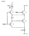
- Fig. 5 is a circuit diagram of each pixel 2 according to this embodiment.
- Each pixel 2 is formed of an organic EL element OLED, four transistors T1, T2, T4, and T5, and a capacitor C.
- the transistors T1, T2, T4, and T5 are p-channel transistors; however, this is merely an example, and the present invention is not limited thereto.
- the first switching transistor T1 has a gate connected with a scanning line to which a scanning signal SEL is supplied, and a source connected with a data line X to which data current Idata is supplied.
- a drain of the first switching transistor T1 is commonly connected with a drain of the control transistor T5, a source of the drive transistor T4, and one electrode of the capacitor C.
- the other electrode of the capacitor C is commonly connected with a gate of the drive transistor T4 and a source of the second switching transistor T2.
- a gate of the second switching transistor T2 is connected with the scanning line to which the scanning signal SEL is supplied.
- a drain of the second switching transistor T2 is commonly connected with a drain of the drive transistor T4 and an anode of the organic EL element OLED.
- a potential Vss is applied to a cathode of the organic EL element OLED.
- a gate of the control transistor T5 is connected with a signal line to which a pulse signal PLS is supplied, and a power potential Vdd is applied to a source of the control transistor T5.
- Fig. 6 is a drive timing chart of each pixel 2 according to this embodiment.
- a current flows in the organic EL element OLED, and the organic EL element OLED emits light.
- one vertical scanning period t0 to t2 can be divided into a programming period t0 to t1 and a driving period t1 to t2.
- the scanning signal SEL falls to the L level, and the switching transistors T1 and T2 are turned on.
- the data line X is electrically connected to the source of the drive transistor T4, and the drive transistor T4 is brought into diode connection, that is, its gate and drain are electrically connected with each other. Therefore, the drive transistor T4 causes the data current Idata supplied from the data line X to flow in the channel thereof, and generates a gate voltage Vg corresponding to the data current Idata at the gate thereof.
- An electric charge corresponding to the generated gate voltage Vg is stored in the capacitor C connected between the gate and source of the drive transistor T4 to write the data. Accordingly, the drive transistor T4 functions as a programming transistor for writing data in the capacitor C for the programming period t0 to t1.
- the pulse signal PLS is maintained at the H level, and the control transistor T5 is off.
- a current path for the driving current Ioled which is formed from the power potential Vdd to the potential Vss is continuously interrupted.
- a current path for the data current Idata is formed between the data line X and the potential Vss via the first switching transistor T1, the drive transistor T4, and the organic EL element OLED. Therefore, the organic EL element OLED still emits light with a brightness corresponding to the data current Idata for the programming period t0 to t1.
- the driving current Ioled corresponding to the electric charge stored in the capacitor C flows in the organic EL element OLED, and the organic EL element OLED emits light.
- the scanning signal SEL rises to the H level, and the switching transistors T1 and T2 are turned off.
- the data line X to which the data current Idata is supplied and the source of the drive transistor T4 are electrically separated from each other, and the gate and drain of the drive transistor T4 are also electrically separated from each other. Due to the electric charge stored in the capacitor C, a voltage equivalent to the gate voltage Vg is applied to the gate of the drive transistor T4.
- the pulse signal PLS which has been kept at the H level, changes to a signal with pulse waveform.
- the control transistor T5 whose conduction is controlled by the pulse signal PLS alternates between the on state and the off state.
- a current path for the driving current Ioled is formed.
- the driving current Ioled flowing in the organic EL element OLED is controlled by the gate voltage Vg related to the electric charge stored in the capacitor C, and the organic EL element OLED emits light with a brightness corresponding to this current level.
- control transistor T5 when the control transistor T5 is in the off state, the current path for the driving current Ioled is forcibly interrupted by the control transistor T5. The conduction of the control transistor T5 is controlled to thereby cause intermittent light emission of the organic EL element OLED for the driving period t to t2.
- the conduction of the control transistor T5 is controlled to thereby repeat interruption of the current path for the driving current Ioled for the period t0 to t2 after the pixel 2 is selected until the next time it is selected.
- light emission and non-light-emission of the organic EL element OLED are carried out a plurality of times for the driving period t1 to t2.
- the optical response of the pixel 2 can be approximately an impulse response.
- the non-light-emission time of the organic EL element OLED (the time of black display) can be dispersed in the period t1 to t2, thus reducing flickering of the displayed image. Therefore, the display quality can be improved.
- the optical response of the pixel 2 can also be further improved, and a false contour in moving pictures can effectively be suppressed.
- the average brightness of light emission and non-light-emission by the organic EL element OLED is lower than that of continuous light emission.
- the balance between the light-emission time and the non-light-emission time can be controlled to thereby perform brightness control with ease.
- intermittent light emission of the organic EL element OLED is carried out by controlling the conduction of the control transistor T5 provided in the current path for the driving current Ioled.
- a second control transistor T6 which is different from the control transistor T5 may be additionally provided in the current path for the driving current Ioled, thus achieving a similar advantage.
- the second control transistor T6 is connected between the drain of the first control transistor T5 and the source of the drive transistor T4.
- the second control transistor T6 is connected between the drain of the drive transistor T4 and the anode of the organic EL element OLED.
- the second control transistor T6 may be, for example, an n-channel transistor having a gate to which the pulse signal PLS is supplied.
- a control signal GP is supplied to the gate of the first control transistor T5.
- Fig. 9 is a drive timing chart of the pixel 2 shown in Fig. 7 or 8.
- the control signal GP is maintained at the H level for the programming period t0 to t1.
- the current path for the driving current Ioled is interrupted a plurality of times by the control transistor T5 whose conduction is controlled by the control signal GP.
- the pulse signal PLS is at the H level, and therefore the second control transistor T6 is turned on.
- a current path for the data current Idata is formed so as to write the data in the capacitor C, and the organic EL element OLED emits light.
- the control signal GP is at the H level, and the pulse signal PLS changes to a signal with pulse waveform.
- the conduction of the second control transistor T6 is controlled by the pulse signal PLS to thereby cause light emission of the organic EL element OLED to be intermittently repeated.
- each horizontal line Y is formed of a single scanning line to which a scanning signal SEL is supplied and a single signal line to which a pulse signal PLS is supplied.
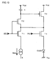
- Fig. 10 is a circuit diagram of each pixel 2 according to this embodiment.
- Each pixel 2 is formed of an organic EL element OLED, four transistors T1, T2, T4, and T5, and a capacitor C.
- the n-channel transistors T1, T2, and T5 and the p-channel transistor T4 are used; however, this is merely an example, and the present invention is not limited thereto.
- the first switching transistor T1 has a gate connected with a scanning line to which a scanning signal SEL is supplied, and a source connected with a data line X to which data current Idata is supplied.
- a drain of the first switching transistor T1 is commonly connected with a source of the second switching transistor T2, a drain of the drive transistor T4, and a drain of the control transistor T5.
- a gate of the second switching transistor T2 is connected with the scanning line to which the scanning signal SEL is supplied.
- a drain of the second switching transistor T2 is commonly connected with one electrode of the capacitor C and a gate of the drive transistor T4.
- a power potential Vdd is applied to the other electrode of the capacitor C and a source of the drive transistor T4.
- the control transistor T5 having a gate to which the pulse signal PLS is supplied is provided between the drain of the drive transistor T4 and an anode of the organic EL element OLED.
- a potential Vss is applied to a cathode of the organic EL element OLED.
- Fig. 11 is a drive timing chart of each pixel 2 according to this embodiment.
- one vertical scanning period 10 to t2 can be divided into a programming period t0 to t1 and a driving period t1 to t2.
- the scanning signal SEL rises to the H level, and the switching transistors T1 and T2 are turned on.
- the data line X and the drain of the drive transistor T4 are electrically connected with each other, and the drive transistor T4 is brought into diode connection, that is, its gate and drain are electrically connected with each other. Therefore, the drive transistor T4 causes the data current Idata supplied from the data line X to flow in the channel thereof, and generates a gate voltage Vg corresponding to the data current Idata at the gate thereof.
- An electric charge corresponding to the generated gate voltage Vg is stored in the capacitor C connected with the gate of the drive transistor T4 to write the data. Accordingly, the drive transistor T4 functions as a programming transistor for writing data in the capacitor C for the programming period t0 to t1.
- the pulse signal PLS is maintained at the L level, and the control transistor T5 is off.
- a current path for the driving current Ioled to the organic EL element OLED is continuously interrupted, and the organic EL element OLED does not emit light for the period t0 to t1.
- the driving current Ioled corresponding to the electric charge stored in the capacitor C flows in the organic EL element OLED, and the organic EL element OLED emits light.
- the scanning signal SEL falls to the L level, and the switching transistors T1 and T2 are turned off.
- the data line X to which the data current Idata is supplied and the drain of the drive transistor T4 are electrically separated from each other, and the gate and drain of the drive transistor T4 are also electrically separated from each other.
- a voltage equivalent to the gate voltage Vg is applied to the gate of the drive transistor T4.
- the pulse signal PLS In synchronization with the fall time of the scanning signal SEL at the time t1, the pulse signal PLS, which has been kept at the L level, changes to a signal with pulse waveform. This pulse waveform continues until the time t2 at which next selection of the pixel 2 starts.
- the control transistor T5 whose conduction is controlled by the pulse signal PLS alternates between the on state and the off state.
- the control transistor T5 When the control transistor T5 is in the on state, a current path for the driving current Ioled is formed, and the organic EL element OLED emits light with a brightness corresponding to the driving current Ioled.
- the control transistor T5 when the control transistor T5 is in the off state, the current path for the driving current Ioled is forcibly interrupted by the control transistor T5.
- the conduction of the control transistor T5 is controlled in this way to thereby cause the current path for the driving current Ioled to be repeatedly interrupted, and light emission and non-light-emission of the organic EL element OLED are
- the conduction of the control transistor T5 is controlled to thereby repeat interruption of the current path for the driving current Ioled for the period t0 to t2 after the pixel 2 is selected until the next time it is selected.
- light emission and non-light-emission of the organic EL element OLED are carried out a plurality of times for the driving period t1 to t2.
- the optical response of the pixel 2 can be approximately an impulse response.
- the non-light-emission time of the organic EL element OLED (the time of black display) can be dispersed in the period t1 to t2, thus reducing flickering of the displayed image. Therefore, the display quality can be improved.
- the optical response of the pixel 2 can also be improved, and a false contour in moving pictures can effectively be suppressed.
- the average brightness of light emission and non-light-emission by the organic EL element OLED is lower than that of continuous light emission.
- the balance between the light-emission time and the non-light-emission time can be controlled to thereby perform brightness control with ease.
- This embodiment relates to a voltage-programmed pixel circuit structure, and particularly to a so-called CC (Conductance Control) method.
- the "voltage-programmed" method refers to a method in which data is supplied to a data line X based on voltage.
- each horizontal line Y is formed of a single scanning line to which a scanning signal SEL is supplied and a single signal line to which a pulse signal PLS is supplied.
- a data voltage Vdata is output directly to the data line X, and therefore the data-line driving circuit 4 does not require a variable current source.
- Fig. 12 is a circuit diagram of each pixel 2 according to this embodiment.
- Each pixel 2 is formed of an organic EL element OLED, three transistors T1, T4, and T5, and a capacitor C.
- the transistors T1, T4, and T5 are n-channel transistors; however, this is merely an example, and the present invention is not limited thereto.
- the switching transistor T1 has a gate connected with a scanning line to which a scanning signal SEL is supplied, and a drain connected with a data line X to which a data voltage Vdata is supplied.
- a source of the switching transistor T1 is commonly connected with one electrode of the capacitor C and a gate of the drive transistor T4.
- a potential Vss is applied to the other electrode of the capacitor C, and a power potential Vdd is applied to a drain of the drive transistor T4.
- the control transistor T5 whose conduction is controlled by the pulse signal PLS has a source connected with an anode of the organic EL element OLED.
- a potential Vss is applied to a cathode of the organic EL element OLED.
- Fig. 13 is a drive timing chart of each pixel 2 according to this embodiment.
- the scanning line SEL rises to the H level, and the switching transistor T1 is turned on.
- the data voltage Vdata supplied to the data line X is applied to one of the electrodes of the capacitor C via the switching transistor T1
- an electric charge corresponding to the data voltage Vdata is stored in the capacitor C (to write data).
- the pulse signal PLS is maintained at the L level, and the control transistor T5 is off Therefore, the current path for the driving current Ioled to the organic EL element OLED is interrupted, and the organic EL element OLED does not emit light for the first half period t0 to t1.
- the driving current Ioled corresponding to the electric charge stored in the capacitor C flows in the organic EL element OLED, and the organic EL element OLED emits light.
- the scanning signal SEL falls to the L level, and the switching transistor T1 is turned off.
- the data voltage Vdata is not applied to one of the electrodes of the capacitor C, but, due to the electric charge stored in the capacitor C, a voltage equivalent to the gate voltage Vg is applied to the gate of the drive transistor T4.
- the pulse signal PLS In synchronization with the fall time of the scanning signal SEL at the time t1, the pulse signal PLS, which has been kept at the L level, changes to a signal with pulse waveform. This pulse waveform continues until the time t2 at which next selection of the pixel 2 starts.
- the conduction of the control transistor T5 is controlled in this way to thereby cause the current path for the driving current Ioled to be interrupted a plurality of times, and light emission and non-light-emission of the organic EL element OLED are therefore repeated.
- the conduction of the control transistor T5 is controlled to thereby repeat interruption of the current path for the driving current Ioled for the period t0 to t2 after the pixel 2 is selected until the next time it is selected.
- light emission and non-light-emission of the organic EL element OLED are carried out a plurality of times for the driving period t 1 to t2.
- the optical response of the pixel 2 can be approximately an impulse response.
- the non-light-emission time of the organic EL element OLED (the time of black display) can be dispersed in the period t1 to t2, thus reducing flickering of the displayed image. Therefore, the display quality can be improved.
- the optical response of the pixel 2 can also be suppressed, and a false contour in moving pictures can effectively removed.
- the average brightness of light emission and non-light-emission by the organic EL element OLED is lower than that of continuous light emission.
- the balance between the light-emission time and the non-light-emission time can be controlled to readily perform brightness control with ease.
- conversion of the waveform of the pulse signal PLS to a pulse form may be started at the same time as the fall time t1 of the scanning signal SEL, or at an earlier time by predetermined time in view of, particularly, stability of low-grayscale data writing.
- each horizontal line Y is formed of two scanning lines to which a first scanning signal and a second scanning signal are supplied, and a single signal line to which a pulse signal PLS is supplied.
- Fig. 14 is a circuit diagram of each pixel 2 according to this embodiment.
- Each pixel 2 is formed of an organic EL element OLED, four transistors T1, T2, T4, and T5, and two capacitors C1 and C2.
- the transistors T1, T2, T4, and T5 are p-channel transistors; however, this is merely an example, and the present invention is not limited thereto.
- the first switching transistor T1 has a gate connected with a scanning line to which a scanning signal SEL is supplied, and a source connected with a data line X to which a data voltage Vdata is supplied.
- a drain of the first switching transistor T1 is connected with one electrode of the first capacitor C1.
- the other electrode of the first capacitor C1 is commonly connected with one electrode of the second capacitor C2, a source of the second switching transistor T2, and a gate of the drive transistor T4.
- a power potential Vdd is applied to the other electrode of the second capacitor C2 and a source of the drive transistor T4.
- a second scanning signal SEL2 is supplied to a gate of the second switching transistor T2, and a drain of the second switching transistor T2 is commonly connected with a drain of the drive transistor T4 and a source of the control transistor T5.
- the control transistor T5 having a gate to which a pulse signal PLS is supplied is provided between the drain of the drive transistor T4 and an anode of the organic EL element OLED.
- a potential Vss is applied to a cathode of the organic EL element OLED.
- Fig. 15 is a drive timing chart of the pixel 2 according to this embodiment.
- One vertical scanning period t0 to t4 can be divided into a period t0 to t1, an auto-zero period t1 to t2, a data loading period t2 to t3, and a driving period t3 to t4.
- the potential of the drain of the drive transistor T4 is set to the potential Vss. More specifically, at the time t0, the first and second scanning signals SEL1 and SEL2 fall to the L level, and the first and second switching transistors T1 and T2 are turned on. Since the power potential Vdd is constantly applied to the data line X for the period t0 to t1, the power potential Vdd is applied to one of the electrodes of the first capacitor C1. In the period t0 to t1, the pulse signal PLS is maintained at the L level, and the control transistor T5 is turned on.
- the gate voltage Vgs of the drive transistor T4 is equal to a threshold voltage Vth.
- the scanning signals SEL1 and SEL2 are still at the L level, and thereby the switching transistors T1 and T2 are still on.
- the pulse signal PLS rises to the H level, and the control transistor T5 is turned off, but the power potential Vdd is still applied to one of the electrodes of the first capacitor C1 from the data line.
- the power potential Vdd applied to the source of the drive transistor T4 is applied to the gate thereof via the channel thereof and the second switching transistor T2.
- the potential difference of the first capacitor C1 is reduced.
- the potential difference of the second capacitor C2 also changes according to the capacitance division between the capacitors C1 and C2.
- the potential difference of each of the capacitors C1 and C2 after changing is determined by a value obtained by deducting the amount of change ⁇ V data from the potential difference (Vdd - Vth) of each capacitor in the auto-zero period t1 to t2. Based on the change in the potential difference of the capacitors C1 and C2 depending upon the amount of change ⁇ V data, data is written to the capacitors C1 and C2.
- the driving current Ioled corresponding to the electric charge stored in the second capacitor C2 flows in the organic EL element OLED, and the organic EL element OLED emits light.
- the first scanning signal SEL1 rises to the H level, and the first switching transistor T1 changes from the on state to the off state (the second switching transistor T2 is still off).
- the voltage of the data line X recovers to the power potential Vdd.
- the data line X to which the data power potential Vdd is applied and one of the electrodes of the first capacitor C1 are separated from each other, and the gate and drain of the drive transistor T4 are also separated from each other.
- a voltage (the gate voltage Vgs based on the source) corresponding to the electric charge stored in the second capacitor C2 is applied to the gate of the drive transistor T4.
- the equation to determine a current Ids (corresponding to the driving current Ioled) flowing in the drive transistor T4 includes the threshold voltage Vth and the gate voltage Vgs of the drive transistor T4 as variables.
- the threshold voltage Vth is cancelled in the equation to determine the driving current Ioled.
- the driving current Ioled is not affected by the threshold voltage Vth of the drive transistor T4, but only depends upon the amount of change ⁇ V data of the data voltage.
- the current path for the driving current Ioled is a path formed from the power potential Vdd to the potential Vss via the drive transistor T4, the control transistor T5, and the organic EL element OLED.
- the driving current Ioled corresponds to the channel current of the drive transistor T4, and is controlled by the gate voltage Vgs related to the electric charge stored in the second capacitor C2.
- the pulse signal PLS is converted to a signal with pulse form, and the control transistor T5 whose conduction is controlled by the signal PLS is alternately turned on and off.
- the current path for the driving current Ioled is repeatedly interrupted, and light emission and non-light-emission of the organic EL element OLED are alternately repeated.
- the control transistor T5 repeats interruption of the current path for the driving current Ioled for the driving period t3 to t4, and continues interruption of the current path for the driving current Ioled for the remaining period t0 to t3 except for the driving period t3 to t4.
- the optical response of the pixel 2 can be approximately an impulse response.
- the non-light-emission time of the organic EL element OLED (the time of black display) can be dispersed in the period t1 to t2, thus reducing flickering of the displayed image. Therefore, the display quality can be further improved.
- the optical response of the pixel 2 can also be improved, and a false contour in moving pictures can effectively be suppressed.
- the average brightness of light emission and non-light-emission by the organic EL element OLED is lower than that of continuous light emission.
- the balance between the light-emission time and the non-light-emission time can be controlled to thereby perform brightness control with ease.
- the pulse waveform of the pulse signal PLS ends at the time t4, but may end at a time a predetermined time earlier than the time t4 in view of, particularly, stability of low-grayscale data writing.
- the electro-optical device may be installed in a variety of electronic apparatuses including, for example, a projector, a cellular phone, a portable terminal, a mobile computer, a personal computer, and so forth. If the above-described electro-optical device is installed in such electronic apparatuses, the commercial value of such electronic apparatuses can be increased, and the electronic apparatuses can have market appeal.
- each pixel having an electro-optical element for emitting light with a brightness corresponding to a driving current includes a control transistor, which is one form of control element, for interrupting a current path for the driving current.
- a control transistor which is one form of control element, for interrupting a current path for the driving current.
Landscapes
- Engineering & Computer Science (AREA)
- Physics & Mathematics (AREA)
- Computer Hardware Design (AREA)
- General Physics & Mathematics (AREA)
- Theoretical Computer Science (AREA)
- Control Of Indicators Other Than Cathode Ray Tubes (AREA)
- Control Of El Displays (AREA)
- Electroluminescent Light Sources (AREA)
Applications Claiming Priority (2)
| Application Number | Priority Date | Filing Date | Title |
|---|---|---|---|
| JP2002360978A JP2004191752A (ja) | 2002-12-12 | 2002-12-12 | 電気光学装置、電気光学装置の駆動方法および電子機器 |
| EP03257710A EP1429312B1 (de) | 2002-12-12 | 2003-12-08 | Elektrooptische Vorrichtung, Verfahren zur Ansteuerung einer elektrooptischen Vorrichtung und elektronisches Gerät |
Related Parent Applications (1)
| Application Number | Title | Priority Date | Filing Date |
|---|---|---|---|
| EP03257710A Division EP1429312B1 (de) | 2002-12-12 | 2003-12-08 | Elektrooptische Vorrichtung, Verfahren zur Ansteuerung einer elektrooptischen Vorrichtung und elektronisches Gerät |
Publications (2)
| Publication Number | Publication Date |
|---|---|
| EP1870875A2 true EP1870875A2 (de) | 2007-12-26 |
| EP1870875A3 EP1870875A3 (de) | 2008-02-20 |
Family
ID=32322124
Family Applications (2)
| Application Number | Title | Priority Date | Filing Date |
|---|---|---|---|
| EP03257710A Expired - Lifetime EP1429312B1 (de) | 2002-12-12 | 2003-12-08 | Elektrooptische Vorrichtung, Verfahren zur Ansteuerung einer elektrooptischen Vorrichtung und elektronisches Gerät |
| EP07075846A Withdrawn EP1870875A3 (de) | 2002-12-12 | 2003-12-08 | Elektrooptische Vorrichtung, Verfahren zur Ansteuerung einer elektrooptischen Vorrichtung und elektronisches Gerät |
Family Applications Before (1)
| Application Number | Title | Priority Date | Filing Date |
|---|---|---|---|
| EP03257710A Expired - Lifetime EP1429312B1 (de) | 2002-12-12 | 2003-12-08 | Elektrooptische Vorrichtung, Verfahren zur Ansteuerung einer elektrooptischen Vorrichtung und elektronisches Gerät |
Country Status (7)
| Country | Link |
|---|---|
| US (3) | US7259735B2 (de) |
| EP (2) | EP1429312B1 (de) |
| JP (1) | JP2004191752A (de) |
| KR (1) | KR100594834B1 (de) |
| CN (2) | CN101127189B (de) |
| DE (1) | DE60317761T2 (de) |
| TW (1) | TWI272569B (de) |
Cited By (4)
| Publication number | Priority date | Publication date | Assignee | Title |
|---|---|---|---|---|
| US7573445B2 (en) | 2002-12-19 | 2009-08-11 | Semiconductor Energy Laboratory Co., Ltd. | Driving method of light emitting device and electronic apparatus |
| US8872868B2 (en) | 2004-09-24 | 2014-10-28 | Semiconductor Energy Laboratory Co., Ltd. | Driving method of light emitting device |
| CN111276097A (zh) * | 2020-03-26 | 2020-06-12 | 京东方科技集团股份有限公司 | 像素驱动电路及其驱动方法、显示基板 |
| US11887535B2 (en) | 2006-10-26 | 2024-01-30 | Semiconductor Energy Laboratory Co., Ltd. | Electronic device, display device, and semiconductor device and method for driving the same |
Families Citing this family (176)
| Publication number | Priority date | Publication date | Assignee | Title |
|---|---|---|---|---|
| US7569849B2 (en) | 2001-02-16 | 2009-08-04 | Ignis Innovation Inc. | Pixel driver circuit and pixel circuit having the pixel driver circuit |
| CA2419704A1 (en) | 2003-02-24 | 2004-08-24 | Ignis Innovation Inc. | Method of manufacturing a pixel with organic light-emitting diode |
| CA2443206A1 (en) | 2003-09-23 | 2005-03-23 | Ignis Innovation Inc. | Amoled display backplanes - pixel driver circuits, array architecture, and external compensation |
| US7196682B2 (en) * | 2003-09-29 | 2007-03-27 | Wintek Corporation | Driving apparatus and method for active matrix organic light emitting display |
| GB0323622D0 (en) * | 2003-10-09 | 2003-11-12 | Koninkl Philips Electronics Nv | Electroluminescent display-devices |
| KR101054327B1 (ko) * | 2004-04-30 | 2011-08-04 | 엘지디스플레이 주식회사 | 화질 개선을 위한 화소구조를 가지는 전류구동형 능동행렬유기전계발광 디스플레이 장치 |
| JP4834876B2 (ja) * | 2004-06-25 | 2011-12-14 | 京セラ株式会社 | 画像表示装置 |
| CA2472671A1 (en) | 2004-06-29 | 2005-12-29 | Ignis Innovation Inc. | Voltage-programming scheme for current-driven amoled displays |
| CN100363967C (zh) * | 2004-07-14 | 2008-01-23 | 友达光电股份有限公司 | 主动式有机发光显示器的象素驱动电路 |
| KR100592640B1 (ko) * | 2004-07-27 | 2006-06-26 | 삼성에스디아이 주식회사 | 발광 표시장치 및 주사 구동부 |
| KR100590068B1 (ko) * | 2004-07-28 | 2006-06-14 | 삼성에스디아이 주식회사 | 발광 표시 장치와, 그 표시 패널 및 화소 회로 |
| KR100846954B1 (ko) * | 2004-08-30 | 2008-07-17 | 삼성에스디아이 주식회사 | 발광 표시장치와 그의 구동방법 |
| JP4942971B2 (ja) * | 2004-09-24 | 2012-05-30 | 株式会社半導体エネルギー研究所 | 発光装置の駆動方法 |
| JP4400401B2 (ja) | 2004-09-30 | 2010-01-20 | セイコーエプソン株式会社 | 電気光学装置とその駆動方法及び電子機器 |
| KR20070090901A (ko) * | 2004-11-03 | 2007-09-06 | 코닌클리즈케 필립스 일렉트로닉스 엔.브이. | 표시 장치 |
| CA2490858A1 (en) | 2004-12-07 | 2006-06-07 | Ignis Innovation Inc. | Driving method for compensated voltage-programming of amoled displays |
| US10013907B2 (en) | 2004-12-15 | 2018-07-03 | Ignis Innovation Inc. | Method and system for programming, calibrating and/or compensating, and driving an LED display |
| TWI402790B (zh) | 2004-12-15 | 2013-07-21 | Ignis Innovation Inc | 用以程式化,校準及驅動一發光元件顯示器的方法及系統 |
| US9799246B2 (en) | 2011-05-20 | 2017-10-24 | Ignis Innovation Inc. | System and methods for extraction of threshold and mobility parameters in AMOLED displays |
| US9171500B2 (en) | 2011-05-20 | 2015-10-27 | Ignis Innovation Inc. | System and methods for extraction of parasitic parameters in AMOLED displays |
| US10012678B2 (en) | 2004-12-15 | 2018-07-03 | Ignis Innovation Inc. | Method and system for programming, calibrating and/or compensating, and driving an LED display |
| US9280933B2 (en) | 2004-12-15 | 2016-03-08 | Ignis Innovation Inc. | System and methods for extraction of threshold and mobility parameters in AMOLED displays |
| US9275579B2 (en) | 2004-12-15 | 2016-03-01 | Ignis Innovation Inc. | System and methods for extraction of threshold and mobility parameters in AMOLED displays |
| US8576217B2 (en) | 2011-05-20 | 2013-11-05 | Ignis Innovation Inc. | System and methods for extraction of threshold and mobility parameters in AMOLED displays |
| US20140111567A1 (en) | 2005-04-12 | 2014-04-24 | Ignis Innovation Inc. | System and method for compensation of non-uniformities in light emitting device displays |
| KR100602363B1 (ko) * | 2005-01-10 | 2006-07-18 | 삼성에스디아이 주식회사 | 발광제어구동부 및 그를 이용한 발광 표시장치 |
| US7646367B2 (en) * | 2005-01-21 | 2010-01-12 | Semiconductor Energy Laboratory Co., Ltd. | Semiconductor device, display device and electronic apparatus |
| CA2495726A1 (en) | 2005-01-28 | 2006-07-28 | Ignis Innovation Inc. | Locally referenced voltage programmed pixel for amoled displays |
| JP4934964B2 (ja) * | 2005-02-03 | 2012-05-23 | ソニー株式会社 | 表示装置、画素駆動方法 |
| CA2496642A1 (en) | 2005-02-10 | 2006-08-10 | Ignis Innovation Inc. | Fast settling time driving method for organic light-emitting diode (oled) displays based on current programming |
| JP2006259530A (ja) | 2005-03-18 | 2006-09-28 | Seiko Epson Corp | 有機el装置及びその駆動方法並びに電子機器 |
| JP4857586B2 (ja) * | 2005-04-05 | 2012-01-18 | セイコーエプソン株式会社 | 電子回路の駆動方法及び駆動回路、発光装置、並びに電子機器 |
| CN102663977B (zh) | 2005-06-08 | 2015-11-18 | 伊格尼斯创新有限公司 | 用于驱动发光器件显示器的方法和系统 |
| CA2518276A1 (en) * | 2005-09-13 | 2007-03-13 | Ignis Innovation Inc. | Compensation technique for luminance degradation in electro-luminance devices |
| KR101322195B1 (ko) | 2005-09-15 | 2013-11-04 | 가부시키가이샤 한도오따이 에네루기 켄큐쇼 | 표시 장치 및 이의 구동 방법 |
| TWI269255B (en) * | 2006-01-03 | 2006-12-21 | Himax Tech Ltd | Organic light-emitting diode (OLED) display and data driver output stage thereof |
| US7545348B2 (en) * | 2006-01-04 | 2009-06-09 | Tpo Displays Corp. | Pixel unit and display and electronic device utilizing the same |
| WO2007079572A1 (en) * | 2006-01-09 | 2007-07-19 | Ignis Innovation Inc. | Method and system for driving an active matrix display circuit |
| US9269322B2 (en) | 2006-01-09 | 2016-02-23 | Ignis Innovation Inc. | Method and system for driving an active matrix display circuit |
| US9489891B2 (en) | 2006-01-09 | 2016-11-08 | Ignis Innovation Inc. | Method and system for driving an active matrix display circuit |
| JP5250960B2 (ja) * | 2006-01-24 | 2013-07-31 | セイコーエプソン株式会社 | 発光装置および電子機器 |
| CN100543820C (zh) * | 2006-01-24 | 2009-09-23 | 友达光电股份有限公司 | 主动式矩阵有机发光二极管显示器及其驱动方法 |
| KR101209043B1 (ko) * | 2006-01-26 | 2012-12-06 | 삼성디스플레이 주식회사 | 표시 장치의 구동 장치 및 이를 포함하는 표시 장치 |
| KR101230308B1 (ko) * | 2006-02-22 | 2013-02-06 | 삼성디스플레이 주식회사 | 표시 장치 |
| KR100761296B1 (ko) * | 2006-03-17 | 2007-09-27 | 엘지전자 주식회사 | 발광 소자 및 이를 구동하는 방법 |
| JP5058505B2 (ja) * | 2006-03-31 | 2012-10-24 | キヤノン株式会社 | 表示装置 |
| CN101501748B (zh) | 2006-04-19 | 2012-12-05 | 伊格尼斯创新有限公司 | 有源矩阵显示器的稳定驱动设计 |
| KR101197768B1 (ko) * | 2006-05-18 | 2012-11-06 | 엘지디스플레이 주식회사 | 유기전계발광표시장치의 화소 회로 |
| JP5124985B2 (ja) * | 2006-05-23 | 2013-01-23 | ソニー株式会社 | 画像表示装置 |
| KR101279115B1 (ko) * | 2006-06-27 | 2013-06-26 | 엘지디스플레이 주식회사 | 유기전계발광표시장치의 화소 회로 |
| KR101202041B1 (ko) | 2006-06-30 | 2012-11-16 | 더 리젠츠 오브 더 유니버시티 오브 미시간 | 유기발광다이오드 표시소자 및 그 구동방법 |
| KR100852349B1 (ko) * | 2006-07-07 | 2008-08-18 | 삼성에스디아이 주식회사 | 유기전계발광 표시장치 및 그 구동방법 |
| CA2556961A1 (en) | 2006-08-15 | 2008-02-15 | Ignis Innovation Inc. | Oled compensation technique based on oled capacitance |
| TW200811812A (en) * | 2006-08-16 | 2008-03-01 | Tpo Displays Corp | System for displaying image and driving method for organic light-emitting element |
| JP4240097B2 (ja) * | 2006-09-25 | 2009-03-18 | ソニー株式会社 | 画素回路及び表示装置 |
| KR100857672B1 (ko) * | 2007-02-02 | 2008-09-08 | 삼성에스디아이 주식회사 | 유기전계발광표시장치 및 그의 구동방법 |
| JP4737120B2 (ja) * | 2007-03-08 | 2011-07-27 | セイコーエプソン株式会社 | 画素回路の駆動方法、電気光学装置および電子機器 |
| JP5361139B2 (ja) * | 2007-03-09 | 2013-12-04 | キヤノン株式会社 | 表示装置 |
| US20080238892A1 (en) * | 2007-03-28 | 2008-10-02 | Himax Technologies Limited | Pixel circuit |
| US7920110B2 (en) * | 2007-03-28 | 2011-04-05 | Himax Technologies Limited | Pixel circuit |
| US8237447B2 (en) * | 2007-05-11 | 2012-08-07 | Panasonic Ev Energy Co., Ltd. | Apparatus for detecting state of storage device |
| TWI413961B (zh) | 2007-06-05 | 2013-11-01 | 新力股份有限公司 | 顯示面板驅動方法、顯示裝置、顯示面板驅動裝置與電子裝置 |
| JP5251007B2 (ja) * | 2007-06-05 | 2013-07-31 | ソニー株式会社 | 表示パネル駆動方法、表示装置、表示パネル駆動装置及び電子機器 |
| JP5309475B2 (ja) | 2007-06-05 | 2013-10-09 | ソニー株式会社 | 表示パネル駆動方法、表示装置、表示パネル駆動装置及び電子機器 |
| JP5251006B2 (ja) * | 2007-06-05 | 2013-07-31 | ソニー株式会社 | 表示パネル駆動方法、表示装置、表示パネル駆動装置及び電子機器 |
| JP5495510B2 (ja) * | 2007-06-19 | 2014-05-21 | キヤノン株式会社 | 表示装置及びそれを用いた電子機器 |
| JP2009014836A (ja) * | 2007-07-02 | 2009-01-22 | Canon Inc | アクティブマトリクス型表示装置及びその駆動方法 |
| CN101779229B (zh) * | 2007-08-21 | 2012-11-07 | 佳能株式会社 | 显示装置及其驱动方法 |
| JP2009080272A (ja) * | 2007-09-26 | 2009-04-16 | Canon Inc | アクティブマトリクス型表示装置 |
| US20090091264A1 (en) * | 2007-10-04 | 2009-04-09 | Himax Technologies Limited | Pixel circuit |
| JP2009109641A (ja) * | 2007-10-29 | 2009-05-21 | Canon Inc | 駆動回路、及びアクティブマトリクス型表示装置 |
| JP4715849B2 (ja) | 2008-01-15 | 2011-07-06 | ソニー株式会社 | 表示装置及びその駆動方法と電子機器 |
| TW200949807A (en) | 2008-04-18 | 2009-12-01 | Ignis Innovation Inc | System and driving method for light emitting device display |
| TWI383355B (zh) * | 2008-05-27 | 2013-01-21 | Univ Nat Cheng Kung | A driving circuit and a pixel circuit having the driving circuit |
| JP4816686B2 (ja) | 2008-06-06 | 2011-11-16 | ソニー株式会社 | 走査駆動回路 |
| JP2010008521A (ja) * | 2008-06-25 | 2010-01-14 | Sony Corp | 表示装置 |
| CA2637343A1 (en) | 2008-07-29 | 2010-01-29 | Ignis Innovation Inc. | Improving the display source driver |
| US8599222B2 (en) | 2008-09-04 | 2013-12-03 | Seiko Epson Corporation | Method of driving pixel circuit, light emitting device, and electronic apparatus |
| US8686660B2 (en) * | 2008-12-05 | 2014-04-01 | Koninklijke Philips N.V. | OLED with integrated delay structure |
| US9370075B2 (en) | 2008-12-09 | 2016-06-14 | Ignis Innovation Inc. | System and method for fast compensation programming of pixels in a display |
| JP2010243938A (ja) * | 2009-04-09 | 2010-10-28 | Sony Corp | 表示装置およびその駆動方法 |
| CA2688870A1 (en) | 2009-11-30 | 2011-05-30 | Ignis Innovation Inc. | Methode and techniques for improving display uniformity |
| US9384698B2 (en) | 2009-11-30 | 2016-07-05 | Ignis Innovation Inc. | System and methods for aging compensation in AMOLED displays |
| CA2669367A1 (en) | 2009-06-16 | 2010-12-16 | Ignis Innovation Inc | Compensation technique for color shift in displays |
| US10319307B2 (en) | 2009-06-16 | 2019-06-11 | Ignis Innovation Inc. | Display system with compensation techniques and/or shared level resources |
| US9311859B2 (en) | 2009-11-30 | 2016-04-12 | Ignis Innovation Inc. | Resetting cycle for aging compensation in AMOLED displays |
| JP5284198B2 (ja) * | 2009-06-30 | 2013-09-11 | キヤノン株式会社 | 表示装置およびその駆動方法 |
| JP2011013415A (ja) * | 2009-07-01 | 2011-01-20 | Canon Inc | アクティブマトリックス型表示装置 |
| JP2011028135A (ja) * | 2009-07-29 | 2011-02-10 | Canon Inc | 表示装置及びその駆動方法 |
| CN101989000B (zh) * | 2009-07-30 | 2012-05-30 | 华映视讯(吴江)有限公司 | 色彩序列液晶显示器及其液晶显示面板驱动方法 |
| GB2474877A (en) * | 2009-10-29 | 2011-05-04 | Dalmatic Lystrup As | Adjustable safety barrier transmitter |
| US8633873B2 (en) | 2009-11-12 | 2014-01-21 | Ignis Innovation Inc. | Stable fast programming scheme for displays |
| US10996258B2 (en) | 2009-11-30 | 2021-05-04 | Ignis Innovation Inc. | Defect detection and correction of pixel circuits for AMOLED displays |
| US8803417B2 (en) | 2009-12-01 | 2014-08-12 | Ignis Innovation Inc. | High resolution pixel architecture |
| CA2687631A1 (en) | 2009-12-06 | 2011-06-06 | Ignis Innovation Inc | Low power driving scheme for display applications |
| US10089921B2 (en) | 2010-02-04 | 2018-10-02 | Ignis Innovation Inc. | System and methods for extracting correlation curves for an organic light emitting device |
| US10176736B2 (en) | 2010-02-04 | 2019-01-08 | Ignis Innovation Inc. | System and methods for extracting correlation curves for an organic light emitting device |
| US10163401B2 (en) | 2010-02-04 | 2018-12-25 | Ignis Innovation Inc. | System and methods for extracting correlation curves for an organic light emitting device |
| US20140313111A1 (en) | 2010-02-04 | 2014-10-23 | Ignis Innovation Inc. | System and methods for extracting correlation curves for an organic light emitting device |
| CA2692097A1 (en) | 2010-02-04 | 2011-08-04 | Ignis Innovation Inc. | Extracting correlation curves for light emitting device |
| US9881532B2 (en) | 2010-02-04 | 2018-01-30 | Ignis Innovation Inc. | System and method for extracting correlation curves for an organic light emitting device |
| CA2696778A1 (en) | 2010-03-17 | 2011-09-17 | Ignis Innovation Inc. | Lifetime, uniformity, parameter extraction methods |
| JP2012128407A (ja) * | 2010-11-24 | 2012-07-05 | Canon Inc | 有機el表示装置 |
| US8907991B2 (en) | 2010-12-02 | 2014-12-09 | Ignis Innovation Inc. | System and methods for thermal compensation in AMOLED displays |
| US20140368491A1 (en) | 2013-03-08 | 2014-12-18 | Ignis Innovation Inc. | Pixel circuits for amoled displays |
| US9351368B2 (en) | 2013-03-08 | 2016-05-24 | Ignis Innovation Inc. | Pixel circuits for AMOLED displays |
| US9606607B2 (en) | 2011-05-17 | 2017-03-28 | Ignis Innovation Inc. | Systems and methods for display systems with dynamic power control |
| WO2012156942A1 (en) | 2011-05-17 | 2012-11-22 | Ignis Innovation Inc. | Systems and methods for display systems with dynamic power control |
| US9886899B2 (en) | 2011-05-17 | 2018-02-06 | Ignis Innovation Inc. | Pixel Circuits for AMOLED displays |
| US9530349B2 (en) | 2011-05-20 | 2016-12-27 | Ignis Innovations Inc. | Charged-based compensation and parameter extraction in AMOLED displays |
| US9466240B2 (en) | 2011-05-26 | 2016-10-11 | Ignis Innovation Inc. | Adaptive feedback system for compensating for aging pixel areas with enhanced estimation speed |
| US9773439B2 (en) | 2011-05-27 | 2017-09-26 | Ignis Innovation Inc. | Systems and methods for aging compensation in AMOLED displays |
| EP2715711A4 (de) | 2011-05-28 | 2014-12-24 | Ignis Innovation Inc | System und verfahren zur schnellen kompensationsprogrammierung von pixeln auf einer anzeige |
| US8901579B2 (en) | 2011-08-03 | 2014-12-02 | Ignis Innovation Inc. | Organic light emitting diode and method of manufacturing |
| US9070775B2 (en) | 2011-08-03 | 2015-06-30 | Ignis Innovations Inc. | Thin film transistor |
| US10089924B2 (en) | 2011-11-29 | 2018-10-02 | Ignis Innovation Inc. | Structural and low-frequency non-uniformity compensation |
| US9385169B2 (en) | 2011-11-29 | 2016-07-05 | Ignis Innovation Inc. | Multi-functional active matrix organic light-emitting diode display |
| US9324268B2 (en) | 2013-03-15 | 2016-04-26 | Ignis Innovation Inc. | Amoled displays with multiple readout circuits |
| JP6124573B2 (ja) | 2011-12-20 | 2017-05-10 | キヤノン株式会社 | 表示装置 |
| US8937632B2 (en) | 2012-02-03 | 2015-01-20 | Ignis Innovation Inc. | Driving system for active-matrix displays |
| US9747834B2 (en) | 2012-05-11 | 2017-08-29 | Ignis Innovation Inc. | Pixel circuits including feedback capacitors and reset capacitors, and display systems therefore |
| US8922544B2 (en) | 2012-05-23 | 2014-12-30 | Ignis Innovation Inc. | Display systems with compensation for line propagation delay |
| US9786223B2 (en) | 2012-12-11 | 2017-10-10 | Ignis Innovation Inc. | Pixel circuits for AMOLED displays |
| US9336717B2 (en) | 2012-12-11 | 2016-05-10 | Ignis Innovation Inc. | Pixel circuits for AMOLED displays |
| CN103021339B (zh) * | 2012-12-31 | 2015-09-16 | 昆山工研院新型平板显示技术中心有限公司 | 像素电路、显示装置及其驱动方法 |
| US9171504B2 (en) | 2013-01-14 | 2015-10-27 | Ignis Innovation Inc. | Driving scheme for emissive displays providing compensation for driving transistor variations |
| US9830857B2 (en) | 2013-01-14 | 2017-11-28 | Ignis Innovation Inc. | Cleaning common unwanted signals from pixel measurements in emissive displays |
| CA2894717A1 (en) | 2015-06-19 | 2016-12-19 | Ignis Innovation Inc. | Optoelectronic device characterization in array with shared sense line |
| US9721505B2 (en) | 2013-03-08 | 2017-08-01 | Ignis Innovation Inc. | Pixel circuits for AMOLED displays |
| EP3043338A1 (de) | 2013-03-14 | 2016-07-13 | Ignis Innovation Inc. | Neuinterpolation mit kantendetektion zur extraktion eines alterungsmusters für amoled-anzeigen |
| WO2014140992A1 (en) | 2013-03-15 | 2014-09-18 | Ignis Innovation Inc. | Dynamic adjustment of touch resolutions on an amoled display |
| CN105144361B (zh) | 2013-04-22 | 2019-09-27 | 伊格尼斯创新公司 | 用于oled显示面板的检测系统 |
| DE112014003719T5 (de) | 2013-08-12 | 2016-05-19 | Ignis Innovation Inc. | Kompensationsgenauigkeit |
| KR102154709B1 (ko) * | 2013-11-08 | 2020-09-11 | 삼성디스플레이 주식회사 | 유기 발광 표시 장치, 및 유기 발광 표시 장치의 리페어 방법 |
| US9761170B2 (en) | 2013-12-06 | 2017-09-12 | Ignis Innovation Inc. | Correction for localized phenomena in an image array |
| US9741282B2 (en) | 2013-12-06 | 2017-08-22 | Ignis Innovation Inc. | OLED display system and method |
| US9502653B2 (en) | 2013-12-25 | 2016-11-22 | Ignis Innovation Inc. | Electrode contacts |
| US10997901B2 (en) | 2014-02-28 | 2021-05-04 | Ignis Innovation Inc. | Display system |
| US10176752B2 (en) | 2014-03-24 | 2019-01-08 | Ignis Innovation Inc. | Integrated gate driver |
| DE102015206281A1 (de) | 2014-04-08 | 2015-10-08 | Ignis Innovation Inc. | Anzeigesystem mit gemeinsam genutzten Niveauressourcen für tragbare Vorrichtungen |
| CN104064149B (zh) | 2014-07-07 | 2016-07-06 | 深圳市华星光电技术有限公司 | 像素电路、具备该像素电路的显示面板和显示器 |
| KR102284840B1 (ko) * | 2014-11-13 | 2021-08-04 | 엘지디스플레이 주식회사 | 유기발광다이오드 표시장치 |
| CA2872563A1 (en) | 2014-11-28 | 2016-05-28 | Ignis Innovation Inc. | High pixel density array architecture |
| CA2873476A1 (en) | 2014-12-08 | 2016-06-08 | Ignis Innovation Inc. | Smart-pixel display architecture |
| CA2879462A1 (en) | 2015-01-23 | 2016-07-23 | Ignis Innovation Inc. | Compensation for color variation in emissive devices |
| CN104637446B (zh) * | 2015-02-03 | 2017-10-24 | 北京大学深圳研究生院 | 像素电路及其驱动方法和一种显示装置 |
| CA2886862A1 (en) | 2015-04-01 | 2016-10-01 | Ignis Innovation Inc. | Adjusting display brightness for avoiding overheating and/or accelerated aging |
| CA2889870A1 (en) | 2015-05-04 | 2016-11-04 | Ignis Innovation Inc. | Optical feedback system |
| CA2892714A1 (en) | 2015-05-27 | 2016-11-27 | Ignis Innovation Inc | Memory bandwidth reduction in compensation system |
| CA2898282A1 (en) | 2015-07-24 | 2017-01-24 | Ignis Innovation Inc. | Hybrid calibration of current sources for current biased voltage progra mmed (cbvp) displays |
| US10657895B2 (en) | 2015-07-24 | 2020-05-19 | Ignis Innovation Inc. | Pixels and reference circuits and timing techniques |
| US10373554B2 (en) | 2015-07-24 | 2019-08-06 | Ignis Innovation Inc. | Pixels and reference circuits and timing techniques |
| CA2900170A1 (en) | 2015-08-07 | 2017-02-07 | Gholamreza Chaji | Calibration of pixel based on improved reference values |
| CA2908285A1 (en) | 2015-10-14 | 2017-04-14 | Ignis Innovation Inc. | Driver with multiple color pixel structure |
| CA2909813A1 (en) | 2015-10-26 | 2017-04-26 | Ignis Innovation Inc | High ppi pattern orientation |
| KR102570950B1 (ko) * | 2015-12-28 | 2023-08-25 | 엘지디스플레이 주식회사 | 개인 몰입형 장치의 표시장치 |
| JP6733361B2 (ja) * | 2016-06-28 | 2020-07-29 | セイコーエプソン株式会社 | 表示装置及び電子機器 |
| JP6812760B2 (ja) | 2016-11-15 | 2021-01-13 | セイコーエプソン株式会社 | 電気光学装置、電子機器、および電気光学装置の駆動方法 |
| US10586491B2 (en) | 2016-12-06 | 2020-03-10 | Ignis Innovation Inc. | Pixel circuits for mitigation of hysteresis |
| KR102309599B1 (ko) | 2017-04-11 | 2021-10-08 | 삼성디스플레이 주식회사 | 유기전계발광 표시장치 |
| US10714018B2 (en) | 2017-05-17 | 2020-07-14 | Ignis Innovation Inc. | System and method for loading image correction data for displays |
| US11025899B2 (en) | 2017-08-11 | 2021-06-01 | Ignis Innovation Inc. | Optical correction systems and methods for correcting non-uniformity of emissive display devices |
| CN107560769A (zh) * | 2017-08-23 | 2018-01-09 | 上海交通大学 | 一种基于薄层面光源与压敏漆的全场压力测试系统 |
| KR102462008B1 (ko) * | 2017-09-22 | 2022-11-03 | 삼성디스플레이 주식회사 | 유기 발광 표시 장치 |
| KR102555144B1 (ko) * | 2017-12-29 | 2023-07-12 | 엘지디스플레이 주식회사 | 디스플레이 장치 |
| US10971078B2 (en) | 2018-02-12 | 2021-04-06 | Ignis Innovation Inc. | Pixel measurement through data line |
| KR102632905B1 (ko) * | 2018-07-18 | 2024-02-06 | 삼성디스플레이 주식회사 | 유기 발광 표시 장치 및 이의 구동 방법 |
| CN108877680A (zh) * | 2018-08-30 | 2018-11-23 | 京东方科技集团股份有限公司 | 一种像素电路及其驱动方法、显示面板及显示装置 |
| CN114651298B (zh) * | 2019-10-17 | 2023-08-01 | 夏普株式会社 | 显示装置 |
| CN111164669A (zh) * | 2019-12-19 | 2020-05-15 | 重庆康佳光电技术研究院有限公司 | 一种电激发光显示器、像素补偿电路及其电压补偿方法 |
| CN111540303A (zh) * | 2020-01-17 | 2020-08-14 | 重庆康佳光电技术研究院有限公司 | 一种驱动电路及显示装置 |
| TWI747550B (zh) * | 2020-10-12 | 2021-11-21 | 友達光電股份有限公司 | 畫素電路及顯示裝置 |
| CN112542144A (zh) * | 2020-12-02 | 2021-03-23 | Tcl华星光电技术有限公司 | 面板驱动电路和显示面板 |
| EP4016516A1 (de) * | 2020-12-18 | 2022-06-22 | Imec VZW | Pixelschaltung |
| CN112837654A (zh) * | 2021-03-22 | 2021-05-25 | 上海天马有机发光显示技术有限公司 | 一种像素电路及其驱动方法、显示面板和显示装置 |
| CN114708828B (zh) * | 2022-04-29 | 2023-05-30 | 深圳市华星光电半导体显示技术有限公司 | 像素电路及显示面板 |
Family Cites Families (16)
| Publication number | Priority date | Publication date | Assignee | Title |
|---|---|---|---|---|
| US5714968A (en) | 1994-08-09 | 1998-02-03 | Nec Corporation | Current-dependent light-emitting element drive circuit for use in active matrix display device |
| WO1998048403A1 (en) | 1997-04-23 | 1998-10-29 | Sarnoff Corporation | Active matrix light emitting diode pixel structure and method |
| JP3686769B2 (ja) * | 1999-01-29 | 2005-08-24 | 日本電気株式会社 | 有機el素子駆動装置と駆動方法 |
| JP4092857B2 (ja) * | 1999-06-17 | 2008-05-28 | ソニー株式会社 | 画像表示装置 |
| JP2001108962A (ja) * | 1999-10-04 | 2001-04-20 | Hitachi Ltd | 液晶表示装置およびその駆動方法 |
| JP2001147659A (ja) * | 1999-11-18 | 2001-05-29 | Sony Corp | 表示装置 |
| JP4040826B2 (ja) * | 2000-06-23 | 2008-01-30 | 株式会社東芝 | 画像処理方法および画像表示システム |
| JP4123711B2 (ja) * | 2000-07-24 | 2008-07-23 | セイコーエプソン株式会社 | 電気光学パネルの駆動方法、電気光学装置、および電子機器 |
| JP3971892B2 (ja) * | 2000-09-08 | 2007-09-05 | 株式会社日立製作所 | 液晶表示装置 |
| US8339339B2 (en) * | 2000-12-26 | 2012-12-25 | Semiconductor Energy Laboratory Co., Ltd. | Light emitting device, method of driving the same, and electronic device |
| KR100370286B1 (ko) * | 2000-12-29 | 2003-01-29 | 삼성에스디아이 주식회사 | 전압구동 유기발광소자의 픽셀회로 |
| TWI248319B (en) * | 2001-02-08 | 2006-01-21 | Semiconductor Energy Lab | Light emitting device and electronic equipment using the same |
| JP2002323873A (ja) * | 2001-02-21 | 2002-11-08 | Semiconductor Energy Lab Co Ltd | 発光装置及び電子機器 |
| JP3608614B2 (ja) * | 2001-03-28 | 2005-01-12 | 株式会社日立製作所 | 表示装置 |
| EP3716257B1 (de) * | 2001-09-07 | 2021-01-20 | Joled Inc. | El-anzeigetafel, verfahren zur ansteuerung davon und el-anzeigevorrichtung |
| JP2003216100A (ja) | 2002-01-21 | 2003-07-30 | Matsushita Electric Ind Co Ltd | El表示パネルとel表示装置およびその駆動方法および表示装置の検査方法とel表示装置のドライバ回路 |
-
2002
- 2002-12-12 JP JP2002360978A patent/JP2004191752A/ja active Pending
-
2003
- 2003-11-14 KR KR1020030080409A patent/KR100594834B1/ko not_active Expired - Fee Related
- 2003-11-17 TW TW092132170A patent/TWI272569B/zh not_active IP Right Cessation
- 2003-11-24 CN CN2007101622187A patent/CN101127189B/zh not_active Expired - Fee Related
- 2003-11-24 CN CNB2003101180573A patent/CN100349199C/zh not_active Expired - Fee Related
- 2003-12-01 US US10/724,263 patent/US7259735B2/en not_active Expired - Fee Related
- 2003-12-08 EP EP03257710A patent/EP1429312B1/de not_active Expired - Lifetime
- 2003-12-08 DE DE60317761T patent/DE60317761T2/de not_active Expired - Lifetime
- 2003-12-08 EP EP07075846A patent/EP1870875A3/de not_active Withdrawn
-
2007
- 2007-07-13 US US11/826,282 patent/US20070257867A1/en not_active Abandoned
- 2007-07-13 US US11/826,287 patent/US7999770B2/en not_active Expired - Fee Related
Cited By (4)
| Publication number | Priority date | Publication date | Assignee | Title |
|---|---|---|---|---|
| US7573445B2 (en) | 2002-12-19 | 2009-08-11 | Semiconductor Energy Laboratory Co., Ltd. | Driving method of light emitting device and electronic apparatus |
| US8872868B2 (en) | 2004-09-24 | 2014-10-28 | Semiconductor Energy Laboratory Co., Ltd. | Driving method of light emitting device |
| US11887535B2 (en) | 2006-10-26 | 2024-01-30 | Semiconductor Energy Laboratory Co., Ltd. | Electronic device, display device, and semiconductor device and method for driving the same |
| CN111276097A (zh) * | 2020-03-26 | 2020-06-12 | 京东方科技集团股份有限公司 | 像素驱动电路及其驱动方法、显示基板 |
Also Published As
| Publication number | Publication date |
|---|---|
| US20070257867A1 (en) | 2007-11-08 |
| DE60317761D1 (de) | 2008-01-10 |
| US7999770B2 (en) | 2011-08-16 |
| CN100349199C (zh) | 2007-11-14 |
| CN101127189A (zh) | 2008-02-20 |
| EP1429312B1 (de) | 2007-11-28 |
| US7259735B2 (en) | 2007-08-21 |
| TW200419506A (en) | 2004-10-01 |
| KR20040051500A (ko) | 2004-06-18 |
| EP1870875A3 (de) | 2008-02-20 |
| JP2004191752A (ja) | 2004-07-08 |
| DE60317761T2 (de) | 2008-11-20 |
| CN101127189B (zh) | 2010-11-10 |
| CN1506931A (zh) | 2004-06-23 |
| US20040150595A1 (en) | 2004-08-05 |
| EP1429312A2 (de) | 2004-06-16 |
| US20070257868A1 (en) | 2007-11-08 |
| EP1429312A3 (de) | 2005-03-30 |
| TWI272569B (en) | 2007-02-01 |
| KR100594834B1 (ko) | 2006-06-30 |
Similar Documents
| Publication | Publication Date | Title |
|---|---|---|
| EP1429312B1 (de) | Elektrooptische Vorrichtung, Verfahren zur Ansteuerung einer elektrooptischen Vorrichtung und elektronisches Gerät | |
| US7283108B2 (en) | Electro-optical device, method of driving electro-optical device, and electronic apparatus | |
| JP4023335B2 (ja) | 電気光学装置、電気光学装置の駆動方法および電子機器 | |
| CN109584808B (zh) | 像素驱动电路、显示装置及驱动方法 | |
| CN101916546B (zh) | 电光学装置、电光学装置的驱动方法以及电子机器 | |
| CN101097677B (zh) | 显示装置及其驱动方法 | |
| KR100897171B1 (ko) | 유기전계발광 표시장치 | |
| KR100667664B1 (ko) | 화소 회로의 구동 방법, 화소 회로 및 전자 기기 | |
| CN101436381B (zh) | 显示装置及其驱动方法和电子设备 | |
| JP2006133731A (ja) | 発光表示装置及びその駆動方法 | |
| JP2006330664A (ja) | 発光表示装置及び発光表示装置の駆動方法 | |
| JP5162807B2 (ja) | 電気光学装置及び電子機器 | |
| JP4412398B2 (ja) | 電気光学装置、電気光学装置の駆動方法および電子機器 | |
| JP4075922B2 (ja) | 電気光学装置、電気光学装置の駆動方法および電子機器 | |
| JP4107101B2 (ja) | 電気光学装置、電気光学装置の駆動方法および電子機器 | |
| JP2004325885A (ja) | 電気光学装置、電気光学装置の駆動方法および電子機器 | |
| JP2009048212A (ja) | 電気光学装置、電気光学装置の駆動方法および電子機器 |
Legal Events
| Date | Code | Title | Description |
|---|---|---|---|
| PUAI | Public reference made under article 153(3) epc to a published international application that has entered the european phase |
Free format text: ORIGINAL CODE: 0009012 |
|
| 17P | Request for examination filed |
Effective date: 20071017 |
|
| AC | Divisional application: reference to earlier application |
Ref document number: 1429312 Country of ref document: EP Kind code of ref document: P |
|
| AK | Designated contracting states |
Kind code of ref document: A2 Designated state(s): DE FR GB |
|
| PUAL | Search report despatched |
Free format text: ORIGINAL CODE: 0009013 |
|
| AK | Designated contracting states |
Kind code of ref document: A3 Designated state(s): DE FR GB |
|
| 17Q | First examination report despatched |
Effective date: 20080328 |
|
| AKX | Designation fees paid |
Designated state(s): DE FR GB |
|
| GRAP | Despatch of communication of intention to grant a patent |
Free format text: ORIGINAL CODE: EPIDOSNIGR1 |
|
| STAA | Information on the status of an ep patent application or granted ep patent |
Free format text: STATUS: THE APPLICATION IS DEEMED TO BE WITHDRAWN |
|
| 18D | Application deemed to be withdrawn |
Effective date: 20091203 |