EP1870876A2 - Apparatus and method for driving liquid crystal display device - Google Patents
Apparatus and method for driving liquid crystal display device Download PDFInfo
- Publication number
- EP1870876A2 EP1870876A2 EP06125134A EP06125134A EP1870876A2 EP 1870876 A2 EP1870876 A2 EP 1870876A2 EP 06125134 A EP06125134 A EP 06125134A EP 06125134 A EP06125134 A EP 06125134A EP 1870876 A2 EP1870876 A2 EP 1870876A2
- Authority
- EP
- European Patent Office
- Prior art keywords
- data
- input data
- signal
- output signal
- accordance
- Prior art date
- Legal status (The legal status is an assumption and is not a legal conclusion. Google has not performed a legal analysis and makes no representation as to the accuracy of the status listed.)
- Granted
Links
Images


Classifications
-
- G—PHYSICS
- G09—EDUCATION; CRYPTOGRAPHY; DISPLAY; ADVERTISING; SEALS
- G09G—ARRANGEMENTS OR CIRCUITS FOR CONTROL OF INDICATING DEVICES USING STATIC MEANS TO PRESENT VARIABLE INFORMATION
- G09G3/00—Control arrangements or circuits, of interest only in connection with visual indicators other than cathode-ray tubes
- G09G3/20—Control arrangements or circuits, of interest only in connection with visual indicators other than cathode-ray tubes for presentation of an assembly of a number of characters, e.g. a page, by composing the assembly by combination of individual elements arranged in a matrix no fixed position being assigned to or needed to be assigned to the individual characters or partial characters
- G09G3/34—Control arrangements or circuits, of interest only in connection with visual indicators other than cathode-ray tubes for presentation of an assembly of a number of characters, e.g. a page, by composing the assembly by combination of individual elements arranged in a matrix no fixed position being assigned to or needed to be assigned to the individual characters or partial characters by control of light from an independent source
- G09G3/36—Control arrangements or circuits, of interest only in connection with visual indicators other than cathode-ray tubes for presentation of an assembly of a number of characters, e.g. a page, by composing the assembly by combination of individual elements arranged in a matrix no fixed position being assigned to or needed to be assigned to the individual characters or partial characters by control of light from an independent source using liquid crystals
- G09G3/3611—Control of matrices with row and column drivers
- G09G3/3685—Details of drivers for data electrodes
-
- G—PHYSICS
- G02—OPTICS
- G02F—OPTICAL DEVICES OR ARRANGEMENTS FOR THE CONTROL OF LIGHT BY MODIFICATION OF THE OPTICAL PROPERTIES OF THE MEDIA OF THE ELEMENTS INVOLVED THEREIN; NON-LINEAR OPTICS; FREQUENCY-CHANGING OF LIGHT; OPTICAL LOGIC ELEMENTS; OPTICAL ANALOGUE/DIGITAL CONVERTERS
- G02F1/00—Devices or arrangements for the control of the intensity, colour, phase, polarisation or direction of light arriving from an independent light source, e.g. switching, gating or modulating; Non-linear optics
- G02F1/01—Devices or arrangements for the control of the intensity, colour, phase, polarisation or direction of light arriving from an independent light source, e.g. switching, gating or modulating; Non-linear optics for the control of the intensity, phase, polarisation or colour
- G02F1/13—Devices or arrangements for the control of the intensity, colour, phase, polarisation or direction of light arriving from an independent light source, e.g. switching, gating or modulating; Non-linear optics for the control of the intensity, phase, polarisation or colour based on liquid crystals, e.g. single liquid crystal display cells
- G02F1/133—Constructional arrangements; Operation of liquid crystal cells; Circuit arrangements
-
- G—PHYSICS
- G09—EDUCATION; CRYPTOGRAPHY; DISPLAY; ADVERTISING; SEALS
- G09G—ARRANGEMENTS OR CIRCUITS FOR CONTROL OF INDICATING DEVICES USING STATIC MEANS TO PRESENT VARIABLE INFORMATION
- G09G3/00—Control arrangements or circuits, of interest only in connection with visual indicators other than cathode-ray tubes
- G09G3/20—Control arrangements or circuits, of interest only in connection with visual indicators other than cathode-ray tubes for presentation of an assembly of a number of characters, e.g. a page, by composing the assembly by combination of individual elements arranged in a matrix no fixed position being assigned to or needed to be assigned to the individual characters or partial characters
-
- G—PHYSICS
- G09—EDUCATION; CRYPTOGRAPHY; DISPLAY; ADVERTISING; SEALS
- G09G—ARRANGEMENTS OR CIRCUITS FOR CONTROL OF INDICATING DEVICES USING STATIC MEANS TO PRESENT VARIABLE INFORMATION
- G09G2310/00—Command of the display device
- G09G2310/06—Details of flat display driving waveforms
-
- G—PHYSICS
- G09—EDUCATION; CRYPTOGRAPHY; DISPLAY; ADVERTISING; SEALS
- G09G—ARRANGEMENTS OR CIRCUITS FOR CONTROL OF INDICATING DEVICES USING STATIC MEANS TO PRESENT VARIABLE INFORMATION
- G09G2320/00—Control of display operating conditions
- G09G2320/02—Improving the quality of display appearance
- G09G2320/0252—Improving the response speed
-
- G—PHYSICS
- G09—EDUCATION; CRYPTOGRAPHY; DISPLAY; ADVERTISING; SEALS
- G09G—ARRANGEMENTS OR CIRCUITS FOR CONTROL OF INDICATING DEVICES USING STATIC MEANS TO PRESENT VARIABLE INFORMATION
- G09G2320/00—Control of display operating conditions
- G09G2320/02—Improving the quality of display appearance
- G09G2320/0271—Adjustment of the gradation levels within the range of the gradation scale, e.g. by redistribution or clipping
- G09G2320/0276—Adjustment of the gradation levels within the range of the gradation scale, e.g. by redistribution or clipping for the purpose of adaptation to the characteristics of a display device, i.e. gamma correction
Definitions
- the present invention relates to a liquid crystal display (LCD) device, and more particularly, to an apparatus and method for driving an LCD device.
- LCD liquid crystal display
- LCD Liquid Crystal Display
- Active matrix type LCD devices have a switching element formed for every liquid crystal cell and are well suited for displaying moving images.
- Thin film transistors (TFTs) are the devices primarily used as the switching element in the active matrix type LCD device.
- LCD devices generally have a relatively slow response speed attributable to the inherent viscosity and elasticity of a liquid crystal, as can be seen from the following Equations 1 and 2: ⁇ r ⁇ ⁇ d 2 ⁇ ⁇ ⁇ ⁇ V a 2 - V F 2 where ⁇ r is a rise time for response to a voltage is applied to the liquid crystal, Va is the applied voltage, V F is a Frederick transition voltage at which liquid crystal molecules start to be inclined, d is a liquid crystal cell gap, and y is the rotational viscosity of the liquid crystal molecules; and ⁇ F ⁇ ⁇ d 2 K where ⁇ F is a falling time for returning the liquid crystal molecules to their original positions by an elastic restoration force after the voltage applied to the liquid crystal is turned off, and K is the inherent elastic modulus of the liquid crystal.
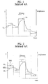
- TN mode LCD device For a twisted nematic (TN) mode LCD device, although the response speed of the liquid crystal may vary with the physical properties and cell gap of the liquid crystal, rise times of 20 to 80ms and the falling times of 20 to 30ms are typical. Because these typical liquid crystal response times are longer than a moving image frame period (for example 16.67ms for moving images according to the National Television Standards Committee (NTSC) standard), the voltage charged on the liquid crystal may not reach the desired level before the next frame data is presented, as shown in FIG. 1. The slow response results in motion blurring in which an afterimage is left on the LCD display panel.
- NTSC National Television Standards Committee
- a related art LCD device may fail to display a desired color and brightness for a moving image because, when data VD is changed from one level to another level, the corresponding display brightness level BL is unable to reach the desired value due to the slow response of the LCD device. As a result, motion blurring occurs in moving images, causing degradation in contrast ratio and display quality.
- U.S. Patent No. 5,495,265 and PCT International Publication No. WO 99/09967 propose a method for modulating data using a look-up table (referred to hereinafter as an 'over-driving method').
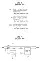
- the principle of this over-driving method of the related art is illustrated in FIG. 2.
- the related art over-driving method includes modulating input data VD to produce modulated data MVD, and applying the modulated data to a liquid crystal cell to obtain a desired brightness level MBL.
- the response speed of a liquid crystal is rapidly accelerated by increasing
- a related art LCD device using the over-driving method is able to compensate for a slow response of a liquid crystal by modulation of a data value to reduce or eliminate motion blurring in a moving image to display a picture having the desired color and brightness.
- the related art over-driving method performs modulation by comparing only respective most significant bits (MSB) of a previous frame (Fn-1) and current frame (Fn) with each other, as shown in FIG. 3.
- the related art over-driving method compares respective most significant bit data (MSB) of the previous frame (Fn-1) and current frame (Fn) with each other to determine whether there is a variation between the two most significant bit data (MSB). If there is a variation between the two most significant bit data (MSB), the corresponding modulated data (MRGB) is selected from a look-up table as most significant bit data (MSB) of the current frame (Fn).
- FIG. 4 illustrates a related art over-driving apparatus implementing the above-described over-driving method.
- the related art over-driving apparatus comprises a frame memory 43 connected to a most significant bit bus line 42, and a look-up table 44 connected in common with the output terminals of the most significant bit bus line 42 and frame memory 43.
- the frame memory 43 stores most significant bit data (MSB) for one frame period and supplies the stored data to the look-up table 44.
- MSB most significant bit data
- the most significant bit data (MSB) includes the four most significant bits of 8-bit source data (RGB).
- the look-up table 44 compares most significant bit data (MSB) of a current frame (Fn) supplied from the most significant bit bus line 42 with most significant bit data (MSB) of a previous frame (Fn-1) inputted from the frame memory 43, as in Table 1 below, and selects modulated data (MRGB) corresponding to the comparison result.
- the modulated data (MRGB) is combined with least significant bit data (LSB) from a least significant bit bus line 41 and then supplied to an LCD device.
- the modulated data (MRGB) registered in the look-up table 44 of the over-driving apparatus and method is as follows: TABLE 1 Current Frame 0 1 2 3 4 5 6 7 8 9 10 11 12 13 14 15 0 0 1 3 4 6 7 9 10 11 12 14 15 15 15 15 15 1 0 1 2 4 5 7 9 10 11 12 13 14 15 15 15 15 2 0 1 2 3 5 7 8 9 10 12 13 14 15 15 15 15 3 0 1 2 3 5 6 8 9 10 11 12 14 14 15 15 15 15 3 0 1 2 3 5 6 8 9 10 11 12 14 14 15 15 15 4 0 0 1 2 4 6 7 9 10 11 12 13 14 15 15 15 15 5 0 0 0 2 3 5 7 8 9 11 12 13 14 15 15 15 15 15 Previous 6 0 0 0 1 3 4 6 8 9 10 11 13 14 15 15 15 15 Frame 7 0 0 0 1 2 4 5 7 8 10 11 12 14 14 15 15 8 0 0 0 1 2 3 5 6 8 9 11 12 13 14 15 15 15 9 0
- Table 1 the leftmost column represents the data voltage (VDn-1) of the previous frame (Fn-1) and the uppermost row represents the data voltage (VDn) of the current frame (Fn).
- the contents of Table 1 are look-up table information obtained by expressing four most significant bits in decimal form.
- the related art apparatus and method for driving the LCD device is used to provide a high response speed of liquid crystal during a gray-to-gray change between previous frame and current frames.
- the gray-to-gray change involves a relatively small voltage difference between frames, so that the liquid crystal response for each gray-to-gray change without overdriving would be slow or non-linear, resulting in poor color change in a moving image or degradation in picture quality.
- a digital memory such as the look-up table 44, is used in the generation of modulated data (MRGB) in the comparison of the data of the previous frame (Fn-1) with that of the current frame (Fn).
- MRGB modulated data
- the use of the digital memory increases chip size as well as manufacturing costs for the LCD device.
- the present invention is directed to an apparatus and method for driving an LCD device, which substantially obviates one or more problems due to limitations and disadvantages of the related art.
- An advantage of the present invention is to provide an apparatus and method for driving an LCD device wherein a response speed of liquid crystal can be increased even without using a memory, thereby preventing degradation in picture quality.
- an apparatus for driving an LCD device includes an image display unit including a plurality of liquid crystal cells formed in areas defined by a plurality of gate and data lines; a gate driver to sequentially supply a scan pulse to the gate lines; a data driver to modulate input data in accordance with the input data, to selectively convert the input data and the modulated input data into an analog video signal, and to supply the analog video signal to the data line; and a timing controller to arrange externally supplied source data, to supply the arranged source data to the data driver, and to control the data driver and the gate driver.
- a method for driving an LCD device having an image display unit including a plurality of liquid crystal cells formed in areas defined by a plurality of gate and data lines includes a first step for sequentially supplying a scan pulse to the gate lines; and a second step for generating modulated input data from input data in accordance with the input data, selectively converting the input data and modulated input data into an analog video signal, and supplying the selected converted analog video signal to the data line.
- FIG. 1 is a waveform diagram illustrating a data-dependent brightness variation in a related art LCD device
- FIG. 2 is a waveform diagram illustrating a data modulation-dependent brightness variation in a related art over-driving method of an LCD device
- FIG. 3 is a view illustrating most significant bit data modulation in a related art over-driving apparatus of an LCD device
- FIG. 4 is a block diagram of the related art over-driving apparatus of an LCD device
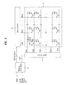
- FIG. 5 is a schematic view illustrating a driving apparatus of an LCD device according to an embodiment of the present invention.
- FIG. 6 is a block diagram schematically illustrating a data driver according to an embodiment of the present invention.
- FIG. 7 is a block diagram schematically illustrating a data output signal generator according to an embodiment of the present invention.
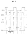
- FIG. 8 is a driving timing view of a data output signal generator shown in FIG. 7;
- FIG. 9 is a block diagram schematically illustrating a modulator according to an embodiment of the present invention.
- FIG. 10 is a waveform diagram illustrating an analog video signal according to an embodiment of the present invention.
- FIG. 5 is a schematic view illustrating a driving apparatus of an LCD device according to an embodiment of the present invention.
- the driving apparatus is provided with an image display unit 2 that includes a plurality of liquid crystal cells respectively formed in areas defined by n gate lines (GL1 to GLn) and m data lines (DL1 to DLm); a gate driver 4 that sequentially supplies a scan pulse to the gate lines (GL1 to GLn); a data driver 6 that converts i-bit input data (Data) to i-bit modulated data to enable rapid response speed of liquid crystal based on at least two most significant bit data of i-bit input data, converts the i-bit modulated data or i-bit input data to an analog video signal, and supplies the analog video signal to the data lines (DL 1 to DLm) in synchronization with the scan pulse; and a timing controller 8 that arranges source data (IZGB) supplied from the external, supplies the arranged source data (RGB) to the data driver 6, and controls the gate driver 4 and the data driver 6.
- IZGB source data supplied from the external, supplies the arranged source data (RGB) to the data driver 6, and controls the
- the image display unit 2 includes a transistor array substrate and a color filter array substrate that are bonded together; spacers to maintain a uniform cell gap between the bonded substrates; and a liquid crystal layer formed in the gap provided between the two bonded substrates and maintained by the spacers.
- the image display unit 2 further includes a plurality of thin film transistors (TFT) formed at the liquid cells defined by n gate lines (GL1 to GLn) and m data lines (DL1 to DLm).
- TFT thin film transistors
- the liquid crystal cells are each connected to a respective TFT.
- the TFTs supply the analog video signals provided from the data lines (DL1 to DLm) to the liquid crystal cells in response to the scan pulse provided from the gate lines (GL 1 to GL,n).
- Each liquid crystal cell can be equivalently represented as a liquid crystal capacitor Clc because each liquid crystal cell is provided with a common electrode facing a pixel electrode connected to the TFT with liquid crystal between the common electrode and the pixel electrode.
- Each liquid crystal cell includes a storage capacitor Cst for maintaining the analog video signal charged on the liquid crystal capacitor Clc until the next analog video signal is charged thereon.
- the timing controller 8 arranges source data (RGB) supplied from a source external to the LCD device to a form appropriate for driving the image display unit 2, and supplies the arranged source data (RGB) to the data driver 6.
- the timing controller 8 generates a data control signal (DCS) and a gate control signal (GCS) using a dot clock signal (DCLK), a data enable signal (DE), and horizontal and vertical synchronous signals (Hsync and Vsync) supplied from an external source, and applies the generated data control signal (DCS) and gate control signal (GCS) respectively to the data and gate drivers 6 and 4, to thereby control the driving timing thereof.
- DCS data control signal
- GCS gate control signal
- the gate driver 4 includes a shift register that generates a scan pulse (gate high signal) in response to the gate control signal (GCS) of the timing controller 8.
- the gate driver 4 sequentially supplies the gate high signal to the gate lines (GL) of the image display unit 2, to thereby turn on the TFTs connected with each gate line (GL).
- the data driver 6 converts i-bit input data (Data) to i-bit modulated data to provide a rapid response speed of liquid crystal based on at least two most significant bits of i-bit input data supplied from the timing controller 8 in response to the data control signal (DCS) supplied from the timing controller 8, converts the i-bit modulated data or i-bit input data to the analog video signal, and supplies the analog video signal for one horizontal line to the data lines (DL1 to DLm) by one horizontal period supplied with the scan pulse.
- the data driver 6 inverts the polarity of the analog video signal supplied to the data lines (DL) in response to a polarity control signal (POL).
- the data driver 6 includes a control block 110, a gamma voltage generator 115, a shift register 120, a latch 130, a modulator 140, a digital-analog converter (DAC) 150, and an output buffer 160.
- a control block 110 for the purpose of supplying the analog video signal, the data driver 6 includes a control block 110, a gamma voltage generator 115, a shift register 120, a latch 130, a modulator 140, a digital-analog converter (DAC) 150, and an output buffer 160.
- DAC digital-analog converter
- the control block 110 supplies the i-bit input data (Data) provided from the timing controller 8 to the latch 130, and supplies the data control signal (DCS) provided from the timing controller 8 to the shift register 120, the latch 130, and the DAC 150.
- the control block 110 supplies a first enable signal (EN1) corresponding to a source start pulse (SSP) and a clock signal (CLK) corresponding to a source shift clock (SSC) to the shift register 120, and outputs a second enable signal (EN2) corresponding to a carry signal (Car) outputted from the shift register 120.
- the control block 110 supplies a source output enable (SOE) to the latch 130, and supplies the polarity control signal (POL) to the DAC 150.
- SOE source output enable
- POL polarity control signal
- the control block 110 includes a data output signal generator that generates first and second data output signals (DOS1 and DOS2) to selectively convert the i-bit modulated data or the i-bit input data to an analog video signal by using the source output enable (SOE) provided from the timing controller 8, and supplies the generated first and second data output signals (DOS1 and DOS2) to the modulator 140.
- DOS1 and DOS2 first and second data output signals
- FIG. 7 is a block diagram schematically illustrating a data output signal generator according to an embodiment of the present invention
- FIG. 8 is a driving timing view of a data output signal generator shown in FIG. 7.
- the data output signal generator 112 includes a source output enable multiply unit 200, a delay unit 210, and first and second data output signal generating units 220 and 230.
- the source output enable multiply unit 200 multiplies the source output enable (SOE) by two, providing two DSOE signals for every single SOE signal, and supplies the multiplied source output enable (DSOE) to the delay unit 210 and the second data output signal generating unit 220, respectively.
- SOE source output enable
- DSOE multiplied source output enable
- the delay unit 210 delays the source output enable (SOE) according to an output signal (DSOE) from the source output enable multiply unit 200, and supplies the delayed signal to the second data output signal generating unit 220. That is, the delay unit 210 delays the source output enable (SOE) according to a rising edge of the multiplied source output enable (DSOE).
- SOE source output enable
- DSOE multiplied source output enable
- the second data output signal generating unit 220 logically operates on the output signal (DSOE) of the source output enable multiply unit 200, and the output signal (DS) of the delay unit 210 to thereby generate the second data output signal (DOS2).
- the second data output signal generating unit 220 may include a NOR-operation gate that generates the second data output signal (DOS2) with a high state only when both of the input signals (DSOE and DS) to the NOR-operation gate are in the low state.
- the first data output signal generating unit 230 logically operates on the source output enable (SOE) and the second data output signal (DOS2) to thereby generate the first data output signal (DOS1).
- the first data output signal generating unit 230 may include a second NOR-operation gate that generates the first data output signal (DOS1) having the high state only when both of the input signals (SOE and DOS2) to the second NOR-operation gate are in the low state.
- the data output signal generator 112 supplies the first data output signal (DOS1) having the high state to the modulator 140 during an initial time period (T1) of the data output of source output enable (SOE) supplied by one horizontal period (1H), and supplies the second data output signal (DOS2) of the high state to the modulator 140 during the remaining time period (T2) excluding the initial time period (T1) on the data output of source output enable (SOE).
- the initial time period (T1) is substantially equal in duration to the remaining time period (T2).
- the gamma voltage generator 115 generates 2 i gamma voltages (GV), each gamma voltage distinct from one another and then supplies the generated 2 i gamma voltages to the DAC 150.
- the distinct gamma voltages may be generated by dividing a gamma reference voltage (GMA) supplied from a gamma reference voltage generator by each of the i-bit gray scale numbers.
- GMA gamma reference voltage
- the shift register 120 generates a sampling signal (Sam) by sequentially shifting the first enable signal (EN1) supplied from the control block 110 in accordance with the clock signal (CLK) of the control block 110, and supplies the sampling signal (Sam) to the latch 130.
- the latch 130 latches i-bit input data (Data), provided from the control block 110, for one horizontal line based on the sampling signal provided from the shift register 120.
- the latch 130 supplies i-bit data (RData) latched for one horizontal line in accordance with the source output enable (SOE) to the modulator 140.
- the modulator 140 includes a gray-scale analyzing unit 310, an addition bit generating unit 320, adding unit 330, and first and second output units 340 and 350.
- the gray-scale analyzing unit 310 analyzes at least two most significant bit data (j) of i-bit latch data (RData) supplied from the latch 130, and supplies a gray-scale analyzing signal (GAS) to the addition bit generating unit 330.
- the gray-scale analyzing unit 310 may generate the gray-scale analyzing signal (GAS) as shown in the following table 2, according to the two most significant bit data of i-bit latch data (RData) supplied from the latch 130. TABLE 2 Two most significant bits Gray-scale analyzing signal (GAS) 00 0 01 1 10 2 11 3
- the addition bit generating unit 320 generates addition bit (ABit) of at least two bits in accordance with the gray-scale analyzing signal (GAS) supplied from the gray-scale analyzing unit 310. For example, as shown in the following table 3, if the gray-scale analyzing signal (GAS) corresponds to '0' or '3', the addition bit generating unit 320 generates the addition bit (ABit) of '001'. If the gray-scale analyzing signal (GAS) corresponds to '1' or '2', the addition bit generating unit 320 generates the addition bit (ABit) of '010'.
- GAS gray-scale analyzing signal
- the following table 3 shows one example of a correspondence between analyzing signal and the generated addition bit (ABit), but the invention may be practicing using correspondences other than that illustrated in table 3.
- the generation of the addition bit (ABit) may be varied to accommodate different resolutions and liquid crystal operating modes of the LCD panel.
- GAS Gray-scale analyzing signal
- Addition bit (ABit) 0 001 1 010 2 010 3 001
- the adding unit 330 adds the addition bit (ABit) of at least two bits provided from the addition bit generating unit 320 to the most significant data of i-bit latch data (RData) provided from the latch 130 to thereby generate i-bit modulated data (MData).
- the adding unit 330 supplies i-bit modulated data (MData) to the first output unit 340. Accordingly, the gray scale of i-bit modulated data (MData) is larger than the gray scale of i-bit latch data (RData).
- the first output unit 340 supplies the i-bit modulated data (MData) provided from the adding unit 330 to the DAC 150.
- the second output unit 350 supplies the i-bit latch data (RData) provided from the latch 130 to the DAC 150.
- the modulator 140 converts the i-bit latch data (RData) into the i-bit modulated data (MData) for the rapid response speed of liquid crystal in accordance with at least two most significant bit data of the i-bit latch data (RData) supplied from the latch 130. After supplying the i-bit modulated data (MData) to the DAC 150 in accordance with the first data output signal (DOS1) of the high state, the modulator 140 supplies the i-bit latch data (RData) to the DAC 150 in accordance with the second data output signal (DOS2) of the high state.
- DOS1 first data output signal
- DOS2 second data output signal
- the modulator 140 For example, if the latch 130 supplies the latch data (RData) of '011000' to the modulator 140, the modulator 140 generates the addition bit (ABit) of '010' according to the gray-scale analyzing signal (GAS) of '1' corresponding to the two most significant bits of '01' in the latch data (RData) of '011000', and adds the addition data (ABit) of '010' to the three most significant bits of the latch data (RData) of '011000', thereby generating modulated data (MData) of '101000'.
- GAS gray-scale analyzing signal
- the modulator 140 supplies the modulated data (MData) of '101000' to the DAC 150 while the first data output signal (DOS1) has a the high state during the initial time period (T1) in the data output period of the source output enable (SOE).
- the modulator 140 supplies the latch data (RData) of '011000' to the DAC 150 while the second data output signal (DOS2) has a the high state during the remaining time period (T2) of the data output period that excludes the initial time period (T1) in the data output period of the source output enable (SOE).
- the DAC 150 selects positive and negative polarity gamma voltages (GV) corresponding to the i-bit modulated data (MData) supplied from the modulator 140 among the 2 i gamma voltages (GV) having the different values supplied from the gamma voltage generator 115, selects one of the positive and negative polarity gamma voltages (GV) based on the polarity control signal (POL) as the analog video signal (Vmdata), and supplies the analog video signal to the output buffer 160.
- MData i-bit modulated data
- POL polarity control signal
- the DAC 150 selects positive and negative polarity gamma voltages (GV) corresponding to the i-bit latch data (RData) supplied from the modulator 140 from the 2' gamma voltages (GV) having the different values supplied from the gamma voltage generator 115, selects one of the positive and negative polarity gamma voltages (GV) based on the polarity control signal (POL) as the analog video signal (Vdata), and supplies the selected voltage to the output buffer 160.
- RData i-bit latch data
- POL polarity control signal
- the output buffer 160 buffers the analog video signal (Vmdata) corresponding to the i-bit modulated data (MData) supplied from the DAC 150, and supplies the buffered signal to the data lines (DL) during the initial time period (T1) in the data output period of the source output enable (SOE).
- the output buffer 160 buffers the analog video data (Vdata) corresponding to the i-bit latch data (RData) supplied from the DAC 150, and supplies the buffered signal to the data lines (DL) during the remaining time period (T2) that excludes the initial time period (T1) in the data output period of the source output enable (SOE).
- the output buffer 160 amplifies and outputs the analog video signal (Vmdata or Vdata) at a suitable level in consideration of the loading on the data lines (DL).
- the data driver 6 drives the liquid crystal cell with the analog video signal (Vmdata) corresponding to the i-bit modulated data (MData) during the initial time period (T1) in the data output of the source output enable (SOE)
- the data driver 6 drives the liquid crystal cell with the analog video signal (Vdata) corresponding to the original i-bit input data (Data) during the remaining time period (T2) that excludes the initial time period (T1) in the data output of the source output enable (SOE).
- the apparatus and method for driving the LCD device according to the present invention may provide the following advantages.
- the liquid crystal cell is previously driven by modulating the input data in accordance with at least two bits of the input data, and then the liquid crystal cell is driven to the desired state in accordance with the original input data.
- the response speed of liquid crystal for the intermediate gray scale may be increased without using the additional memory to prevent the color change or degradation in picture quality. Further, by allowing the omission of additional memory in an apparatus and method for driving the LCD device according to the present invention the fabrication cost of the LCD device can be decreased.
Landscapes
- Engineering & Computer Science (AREA)
- Physics & Mathematics (AREA)
- General Physics & Mathematics (AREA)
- Theoretical Computer Science (AREA)
- Computer Hardware Design (AREA)
- Crystallography & Structural Chemistry (AREA)
- Chemical & Material Sciences (AREA)
- Nonlinear Science (AREA)
- Mathematical Physics (AREA)
- Optics & Photonics (AREA)
- Control Of Indicators Other Than Cathode Ray Tubes (AREA)
- Liquid Crystal (AREA)
- Liquid Crystal Display Device Control (AREA)
Abstract

Description
- This application claims the benefit of
Korean Patent Application No. P2006-56859, filed on June 23, 2006 - The present invention relates to a liquid crystal display (LCD) device, and more particularly, to an apparatus and method for driving an LCD device.
- Liquid Crystal Display (LCD) devices have been used in many different types of electronic equipment. The LCD devices display images by adjusting the light transmittance of liquid crystal cells according to a video signal. Active matrix type LCD devices have a switching element formed for every liquid crystal cell and are well suited for displaying moving images. Thin film transistors (TFTs) are the devices primarily used as the switching element in the active matrix type LCD device.
- However, LCD devices generally have a relatively slow response speed attributable to the inherent viscosity and elasticity of a liquid crystal, as can be seen from the following
Equations 1 and 2:
where τr is a rise time for response to a voltage is applied to the liquid crystal, Va is the applied voltage, VF is a Frederick transition voltage at which liquid crystal molecules start to be inclined, d is a liquid crystal cell gap, and y is the rotational viscosity of the liquid crystal molecules; and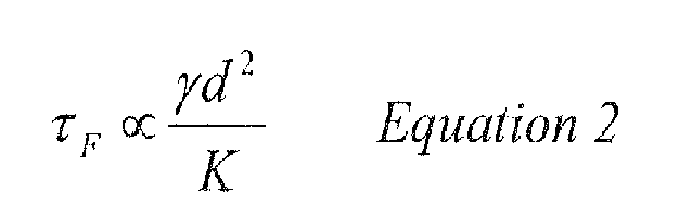
where τF is a falling time for returning the liquid crystal molecules to their original positions by an elastic restoration force after the voltage applied to the liquid crystal is turned off, and K is the inherent elastic modulus of the liquid crystal. - For a twisted nematic (TN) mode LCD device, although the response speed of the liquid crystal may vary with the physical properties and cell gap of the liquid crystal, rise times of 20 to 80ms and the falling times of 20 to 30ms are typical. Because these typical liquid crystal response times are longer than a moving image frame period (for example 16.67ms for moving images according to the National Television Standards Committee (NTSC) standard), the voltage charged on the liquid crystal may not reach the desired level before the next frame data is presented, as shown in FIG. 1. The slow response results in motion blurring in which an afterimage is left on the LCD display panel.
- As illustrated in FIG. 1, a related art LCD device may fail to display a desired color and brightness for a moving image because, when data VD is changed from one level to another level, the corresponding display brightness level BL is unable to reach the desired value due to the slow response of the LCD device. As a result, motion blurring occurs in moving images, causing degradation in contrast ratio and display quality.
- As one method for overcoming the low response speed of the LCD device,
U.S. Patent No. 5,495,265 andPCT International Publication No. WO 99/09967 - As may be appreciated with reference to FIG. 2, the related art over-driving method includes modulating input data VD to produce modulated data MVD, and applying the modulated data to a liquid crystal cell to obtain a desired brightness level MBL. By this method, the response speed of a liquid crystal is rapidly accelerated by increasing |Va 2-VF 2| in the
Equation 1 for a variation in the input data from that of a previous frame period in order to obtain the desired brightness level corresponding to the luminance of the input data in one frame period. - Accordingly, a related art LCD device using the over-driving method is able to compensate for a slow response of a liquid crystal by modulation of a data value to reduce or eliminate motion blurring in a moving image to display a picture having the desired color and brightness.
- In order to reduce the memory storage used in implementing over-driving, the related art over-driving method performs modulation by comparing only respective most significant bits (MSB) of a previous frame (Fn-1) and current frame (Fn) with each other, as shown in FIG. 3. In other words, the related art over-driving method compares respective most significant bit data (MSB) of the previous frame (Fn-1) and current frame (Fn) with each other to determine whether there is a variation between the two most significant bit data (MSB). If there is a variation between the two most significant bit data (MSB), the corresponding modulated data (MRGB) is selected from a look-up table as most significant bit data (MSB) of the current frame (Fn).
- FIG. 4 illustrates a related art over-driving apparatus implementing the above-described over-driving method.
- As illustrated in FIG. 4, the related art over-driving apparatus comprises a
frame memory 43 connected to a most significantbit bus line 42, and a look-up table 44 connected in common with the output terminals of the most significantbit bus line 42 andframe memory 43. - The
frame memory 43 stores most significant bit data (MSB) for one frame period and supplies the stored data to the look-up table 44. In the related art over-driving apparatus of FIG. 4, the most significant bit data (MSB) includes the four most significant bits of 8-bit source data (RGB). - The look-up table 44 compares most significant bit data (MSB) of a current frame (Fn) supplied from the most significant
bit bus line 42 with most significant bit data (MSB) of a previous frame (Fn-1) inputted from theframe memory 43, as in Table 1 below, and selects modulated data (MRGB) corresponding to the comparison result. The modulated data (MRGB) is combined with least significant bit data (LSB) from a least significantbit bus line 41 and then supplied to an LCD device. - Where the most significant bit data (MSB) is limited to four bits, the modulated data (MRGB) registered in the look-up table 44 of the over-driving apparatus and method is as follows:
TABLE 1 Current Frame 0 1 2 3 4 5 6 7 8 9 10 11 12 13 14 15 0 0 1 3 4 6 7 9 10 11 12 14 15 15 15 15 15 1 0 1 2 4 5 7 9 10 11 12 13 14 15 15 15 15 2 0 1 2 3 5 7 8 9 10 12 13 14 15 15 15 15 3 0 1 2 3 5 6 8 9 10 11 12 14 14 15 15 15 4 0 0 1 2 4 6 7 9 10 11 12 13 14 15 15 15 5 0 0 0 2 3 5 7 8 9 11 12 13 14 15 15 15 Previous 6 0 0 0 1 3 4 6 8 9 10 11 13 14 15 15 15 Frame 7 0 0 0 1 2 4 5 7 8 10 11 12 14 14 15 15 8 0 0 0 1 2 3 5 6 8 9 11 12 13 14 15 15 9 0 0 0 1 2 3 4 6 7 9 10 12 13 14 15 15 10 0 0 0 0 1 2 4 5 7 8 10 11 13 14 15 15 11 0 0 0 0 0 2 3 5 6 7 9 11 12 14 15 15 12 0 0 0 0 0 1 3 4 5 7 8 10 12 13 15 15 13 0 0 0 0 0 1 2 3 4 6 8 10 11 13 14 15 14 0 0 0 0 0 0 1 2 3 5 7 9 11 13 14 15 15 0 0 0 0 0 0 0 1 2 4 6 9 11 13 14 15 - In the above Table 1, the leftmost column represents the data voltage (VDn-1) of the previous frame (Fn-1) and the uppermost row represents the data voltage (VDn) of the current frame (Fn). The contents of Table 1 are look-up table information obtained by expressing four most significant bits in decimal form.
- The related art apparatus and method for driving the LCD device is used to provide a high response speed of liquid crystal during a gray-to-gray change between previous frame and current frames. In comparison to the variation associated with a black-to-white change, the gray-to-gray change involves a relatively small voltage difference between frames, so that the liquid crystal response for each gray-to-gray change without overdriving would be slow or non-linear, resulting in poor color change in a moving image or degradation in picture quality.
- In the above-described over-driving apparatus a digital memory, such as the look-up table 44, is used in the generation of modulated data (MRGB) in the comparison of the data of the previous frame (Fn-1) with that of the current frame (Fn). The use of the digital memory increases chip size as well as manufacturing costs for the LCD device.
- Accordingly, the present invention is directed to an apparatus and method for driving an LCD device, which substantially obviates one or more problems due to limitations and disadvantages of the related art.
- An advantage of the present invention is to provide an apparatus and method for driving an LCD device wherein a response speed of liquid crystal can be increased even without using a memory, thereby preventing degradation in picture quality.
- Additional features and advantages of the invention will be set forth in the description which follows, and in part will be apparent from the description, or may be learned by practice of the invention. The objectives and other advantages of the invention will be realized and attained by the structure particularly pointed out in the written description and claims hereof as well as the appended drawings.
- To achieve these objects and other advantages and in accordance with the purpose of the invention, as embodied and broadly described herein, an apparatus for driving an LCD device includes an image display unit including a plurality of liquid crystal cells formed in areas defined by a plurality of gate and data lines; a gate driver to sequentially supply a scan pulse to the gate lines; a data driver to modulate input data in accordance with the input data, to selectively convert the input data and the modulated input data into an analog video signal, and to supply the analog video signal to the data line; and a timing controller to arrange externally supplied source data, to supply the arranged source data to the data driver, and to control the data driver and the gate driver.
- In another aspect of the present invention, a method for driving an LCD device having an image display unit including a plurality of liquid crystal cells formed in areas defined by a plurality of gate and data lines includes a first step for sequentially supplying a scan pulse to the gate lines; and a second step for generating modulated input data from input data in accordance with the input data, selectively converting the input data and modulated input data into an analog video signal, and supplying the selected converted analog video signal to the data line.
- It is to be understood that both the foregoing general description and the following detailed description are exemplary and explanatory and are intended to provide further explanation of the invention as claimed.
- The accompanying drawings, which are included to provide a further understanding of the invention and are incorporated in and constitute a part of this specification, illustrate embodiments of the invention and together with the description serve to explain the principles of the invention.
- In the drawings:
- FIG. 1 is a waveform diagram illustrating a data-dependent brightness variation in a related art LCD device;
- FIG. 2 is a waveform diagram illustrating a data modulation-dependent brightness variation in a related art over-driving method of an LCD device;
- FIG. 3 is a view illustrating most significant bit data modulation in a related art over-driving apparatus of an LCD device;
- FIG. 4 is a block diagram of the related art over-driving apparatus of an LCD device;
- FIG. 5 is a schematic view illustrating a driving apparatus of an LCD device according to an embodiment of the present invention;
- FIG. 6 is a block diagram schematically illustrating a data driver according to an embodiment of the present invention;
- FIG. 7 is a block diagram schematically illustrating a data output signal generator according to an embodiment of the present invention;
- FIG. 8 is a driving timing view of a data output signal generator shown in FIG. 7;
- FIG. 9 is a block diagram schematically illustrating a modulator according to an embodiment of the present invention; and
- FIG. 10 is a waveform diagram illustrating an analog video signal according to an embodiment of the present invention.
- Reference will now be made in detail to embodiments of the present invention, examples of which are illustrated in the accompanying drawings. Wherever possible, the same reference numbers will be used throughout the drawings to refer to the same or like parts.
- Hereinafter, an apparatus and method for driving an LCD device according to the present invention will be explained with reference to the accompanying drawings.
- FIG. 5 is a schematic view illustrating a driving apparatus of an LCD device according to an embodiment of the present invention.
- As shown in FIG. 5, the driving apparatus is provided with an
image display unit 2 that includes a plurality of liquid crystal cells respectively formed in areas defined by n gate lines (GL1 to GLn) and m data lines (DL1 to DLm); agate driver 4 that sequentially supplies a scan pulse to the gate lines (GL1 to GLn); adata driver 6 that converts i-bit input data (Data) to i-bit modulated data to enable rapid response speed of liquid crystal based on at least two most significant bit data of i-bit input data, converts the i-bit modulated data or i-bit input data to an analog video signal, and supplies the analog video signal to the data lines (DL 1 to DLm) in synchronization with the scan pulse; and atiming controller 8 that arranges source data (IZGB) supplied from the external, supplies the arranged source data (RGB) to thedata driver 6, and controls thegate driver 4 and thedata driver 6. - The
image display unit 2 includes a transistor array substrate and a color filter array substrate that are bonded together; spacers to maintain a uniform cell gap between the bonded substrates; and a liquid crystal layer formed in the gap provided between the two bonded substrates and maintained by the spacers. - The
image display unit 2 further includes a plurality of thin film transistors (TFT) formed at the liquid cells defined by n gate lines (GL1 to GLn) and m data lines (DL1 to DLm). The liquid crystal cells are each connected to a respective TFT. The TFTs supply the analog video signals provided from the data lines (DL1 to DLm) to the liquid crystal cells in response to the scan pulse provided from the gate lines (GL 1 to GL,n). - Each liquid crystal cell can be equivalently represented as a liquid crystal capacitor Clc because each liquid crystal cell is provided with a common electrode facing a pixel electrode connected to the TFT with liquid crystal between the common electrode and the pixel electrode. Each liquid crystal cell includes a storage capacitor Cst for maintaining the analog video signal charged on the liquid crystal capacitor Clc until the next analog video signal is charged thereon.
- The
timing controller 8 arranges source data (RGB) supplied from a source external to the LCD device to a form appropriate for driving theimage display unit 2, and supplies the arranged source data (RGB) to thedata driver 6. Thetiming controller 8 generates a data control signal (DCS) and a gate control signal (GCS) using a dot clock signal (DCLK), a data enable signal (DE), and horizontal and vertical synchronous signals (Hsync and Vsync) supplied from an external source, and applies the generated data control signal (DCS) and gate control signal (GCS) respectively to the data andgate drivers - The
gate driver 4 includes a shift register that generates a scan pulse (gate high signal) in response to the gate control signal (GCS) of thetiming controller 8. Thegate driver 4 sequentially supplies the gate high signal to the gate lines (GL) of theimage display unit 2, to thereby turn on the TFTs connected with each gate line (GL). - The
data driver 6 converts i-bit input data (Data) to i-bit modulated data to provide a rapid response speed of liquid crystal based on at least two most significant bits of i-bit input data supplied from thetiming controller 8 in response to the data control signal (DCS) supplied from thetiming controller 8, converts the i-bit modulated data or i-bit input data to the analog video signal, and supplies the analog video signal for one horizontal line to the data lines (DL1 to DLm) by one horizontal period supplied with the scan pulse. Thedata driver 6 inverts the polarity of the analog video signal supplied to the data lines (DL) in response to a polarity control signal (POL). - As shown in FIG. 6, for the purpose of supplying the analog video signal, the
data driver 6 includes acontrol block 110, agamma voltage generator 115, ashift register 120, alatch 130, amodulator 140, a digital-analog converter (DAC) 150, and anoutput buffer 160. - The
control block 110 supplies the i-bit input data (Data) provided from thetiming controller 8 to thelatch 130, and supplies the data control signal (DCS) provided from thetiming controller 8 to theshift register 120, thelatch 130, and theDAC 150. Thecontrol block 110 supplies a first enable signal (EN1) corresponding to a source start pulse (SSP) and a clock signal (CLK) corresponding to a source shift clock (SSC) to theshift register 120, and outputs a second enable signal (EN2) corresponding to a carry signal (Car) outputted from theshift register 120. Thecontrol block 110 supplies a source output enable (SOE) to thelatch 130, and supplies the polarity control signal (POL) to theDAC 150. - The
control block 110 includes a data output signal generator that generates first and second data output signals (DOS1 and DOS2) to selectively convert the i-bit modulated data or the i-bit input data to an analog video signal by using the source output enable (SOE) provided from thetiming controller 8, and supplies the generated first and second data output signals (DOS1 and DOS2) to themodulator 140. - FIG. 7 is a block diagram schematically illustrating a data output signal generator according to an embodiment of the present invention, and FIG. 8 is a driving timing view of a data output signal generator shown in FIG. 7. Referring to FIG. 7 in association with FIG. 8, the data
output signal generator 112 includes a source output enable multiplyunit 200, adelay unit 210, and first and second data outputsignal generating units - The source output enable multiply
unit 200 multiplies the source output enable (SOE) by two, providing two DSOE signals for every single SOE signal, and supplies the multiplied source output enable (DSOE) to thedelay unit 210 and the second data outputsignal generating unit 220, respectively. - The
delay unit 210 delays the source output enable (SOE) according to an output signal (DSOE) from the source output enable multiplyunit 200, and supplies the delayed signal to the second data outputsignal generating unit 220. That is, thedelay unit 210 delays the source output enable (SOE) according to a rising edge of the multiplied source output enable (DSOE). - The second data output
signal generating unit 220 logically operates on the output signal (DSOE) of the source output enable multiplyunit 200, and the output signal (DS) of thedelay unit 210 to thereby generate the second data output signal (DOS2). For example, the second data outputsignal generating unit 220 may include a NOR-operation gate that generates the second data output signal (DOS2) with a high state only when both of the input signals (DSOE and DS) to the NOR-operation gate are in the low state. - The first data output
signal generating unit 230 logically operates on the source output enable (SOE) and the second data output signal (DOS2) to thereby generate the first data output signal (DOS1). For example, the first data outputsignal generating unit 230 may include a second NOR-operation gate that generates the first data output signal (DOS1) having the high state only when both of the input signals (SOE and DOS2) to the second NOR-operation gate are in the low state. - The data
output signal generator 112 supplies the first data output signal (DOS1) having the high state to themodulator 140 during an initial time period (T1) of the data output of source output enable (SOE) supplied by one horizontal period (1H), and supplies the second data output signal (DOS2) of the high state to themodulator 140 during the remaining time period (T2) excluding the initial time period (T1) on the data output of source output enable (SOE). In the illustrated embodiment, the initial time period (T1) is substantially equal in duration to the remaining time period (T2). - In FIG. 6, the
gamma voltage generator 115 generates 2i gamma voltages (GV), each gamma voltage distinct from one another and then supplies the generated 2i gamma voltages to theDAC 150. For example, the distinct gamma voltages may be generated by dividing a gamma reference voltage (GMA) supplied from a gamma reference voltage generator by each of the i-bit gray scale numbers. - The
shift register 120 generates a sampling signal (Sam) by sequentially shifting the first enable signal (EN1) supplied from thecontrol block 110 in accordance with the clock signal (CLK) of thecontrol block 110, and supplies the sampling signal (Sam) to thelatch 130. - The
latch 130 latches i-bit input data (Data), provided from thecontrol block 110, for one horizontal line based on the sampling signal provided from theshift register 120. Thelatch 130 supplies i-bit data (RData) latched for one horizontal line in accordance with the source output enable (SOE) to themodulator 140. - As shown in FIG. 9, the
modulator 140 includes a gray-scale analyzing unit 310, an additionbit generating unit 320, addingunit 330, and first andsecond output units 340 and 350. - The gray-scale analyzing unit 310 analyzes at least two most significant bit data (j) of i-bit latch data (RData) supplied from the
latch 130, and supplies a gray-scale analyzing signal (GAS) to the additionbit generating unit 330. For example, the gray-scale analyzing unit 310 may generate the gray-scale analyzing signal (GAS) as shown in the following table 2, according to the two most significant bit data of i-bit latch data (RData) supplied from thelatch 130.TABLE 2 Two most significant bits Gray-scale analyzing signal (GAS) 00 0 01 1 10 2 11 3 - The addition
bit generating unit 320 generates addition bit (ABit) of at least two bits in accordance with the gray-scale analyzing signal (GAS) supplied from the gray-scale analyzing unit 310. For example, as shown in the following table 3, if the gray-scale analyzing signal (GAS) corresponds to '0' or '3', the additionbit generating unit 320 generates the addition bit (ABit) of '001'. If the gray-scale analyzing signal (GAS) corresponds to '1' or '2', the additionbit generating unit 320 generates the addition bit (ABit) of '010'. The following table 3 shows one example of a correspondence between analyzing signal and the generated addition bit (ABit), but the invention may be practicing using correspondences other than that illustrated in table 3. For example, the generation of the addition bit (ABit) may be varied to accommodate different resolutions and liquid crystal operating modes of the LCD panel.TABLE 3 Gray-scale analyzing signal (GAS) Addition bit (ABit) 0 001 1 010 2 010 3 001 - The adding
unit 330 adds the addition bit (ABit) of at least two bits provided from the additionbit generating unit 320 to the most significant data of i-bit latch data (RData) provided from thelatch 130 to thereby generate i-bit modulated data (MData). The addingunit 330 supplies i-bit modulated data (MData) to the first output unit 340. Accordingly, the gray scale of i-bit modulated data (MData) is larger than the gray scale of i-bit latch data (RData). - In accordance with the first data output signal (DOS1) of the high state, the first output unit 340 supplies the i-bit modulated data (MData) provided from the adding
unit 330 to theDAC 150. In accordance with the second data output signal (DOS2) of the high state, thesecond output unit 350 supplies the i-bit latch data (RData) provided from thelatch 130 to theDAC 150. - The
modulator 140 converts the i-bit latch data (RData) into the i-bit modulated data (MData) for the rapid response speed of liquid crystal in accordance with at least two most significant bit data of the i-bit latch data (RData) supplied from thelatch 130. After supplying the i-bit modulated data (MData) to theDAC 150 in accordance with the first data output signal (DOS1) of the high state, themodulator 140 supplies the i-bit latch data (RData) to theDAC 150 in accordance with the second data output signal (DOS2) of the high state. - For example, if the
latch 130 supplies the latch data (RData) of '011000' to themodulator 140, themodulator 140 generates the addition bit (ABit) of '010' according to the gray-scale analyzing signal (GAS) of '1' corresponding to the two most significant bits of '01' in the latch data (RData) of '011000', and adds the addition data (ABit) of '010' to the three most significant bits of the latch data (RData) of '011000', thereby generating modulated data (MData) of '101000'. - The
modulator 140 supplies the modulated data (MData) of '101000' to theDAC 150 while the first data output signal (DOS1) has a the high state during the initial time period (T1) in the data output period of the source output enable (SOE). Themodulator 140 supplies the latch data (RData) of '011000' to theDAC 150 while the second data output signal (DOS2) has a the high state during the remaining time period (T2) of the data output period that excludes the initial time period (T1) in the data output period of the source output enable (SOE). - Referring again to FIG. 6, the
DAC 150 selects positive and negative polarity gamma voltages (GV) corresponding to the i-bit modulated data (MData) supplied from themodulator 140 among the 2i gamma voltages (GV) having the different values supplied from thegamma voltage generator 115, selects one of the positive and negative polarity gamma voltages (GV) based on the polarity control signal (POL) as the analog video signal (Vmdata), and supplies the analog video signal to theoutput buffer 160. - The
DAC 150 selects positive and negative polarity gamma voltages (GV) corresponding to the i-bit latch data (RData) supplied from the modulator 140 from the 2' gamma voltages (GV) having the different values supplied from thegamma voltage generator 115, selects one of the positive and negative polarity gamma voltages (GV) based on the polarity control signal (POL) as the analog video signal (Vdata), and supplies the selected voltage to theoutput buffer 160. - The
output buffer 160 buffers the analog video signal (Vmdata) corresponding to the i-bit modulated data (MData) supplied from theDAC 150, and supplies the buffered signal to the data lines (DL) during the initial time period (T1) in the data output period of the source output enable (SOE). Theoutput buffer 160 buffers the analog video data (Vdata) corresponding to the i-bit latch data (RData) supplied from theDAC 150, and supplies the buffered signal to the data lines (DL) during the remaining time period (T2) that excludes the initial time period (T1) in the data output period of the source output enable (SOE). Theoutput buffer 160 amplifies and outputs the analog video signal (Vmdata or Vdata) at a suitable level in consideration of the loading on the data lines (DL). - As shown in FIG. 10, after the
data driver 6 previously drives the liquid crystal cell with the analog video signal (Vmdata) corresponding to the i-bit modulated data (MData) during the initial time period (T1) in the data output of the source output enable (SOE), thedata driver 6 drives the liquid crystal cell with the analog video signal (Vdata) corresponding to the original i-bit input data (Data) during the remaining time period (T2) that excludes the initial time period (T1) in the data output of the source output enable (SOE). - As described above, the apparatus and method for driving the LCD device according to the present invention may provide the following advantages.
- In the apparatus and method for driving the LCD device according to the present invention, the liquid crystal cell is previously driven by modulating the input data in accordance with at least two bits of the input data, and then the liquid crystal cell is driven to the desired state in accordance with the original input data.
- Accordingly, the response speed of liquid crystal for the intermediate gray scale may be increased without using the additional memory to prevent the color change or degradation in picture quality. Further, by allowing the omission of additional memory in an apparatus and method for driving the LCD device according to the present invention the fabrication cost of the LCD device can be decreased.
- It will be apparent to those skilled in the art that various modifications and variation can be made in the present invention without departing from the spirit or scope of the invention. Thus, it is intended that the present invention cover the modifications and variations of this invention provided they come within the scope of the appended claims and their equivalents.
Claims (20)
- An apparatus for driving an LCD device comprising:an image display unit including a plurality of liquid crystal cells formed in areas defined by a plurality of gate and data lines;a gate driver to sequentially supply a scan pulse to the gate lines;a data driver to modulate input data in accordance with the input data, to selectively convert the input data and the modulated input data into an analog video signal, and to supply the analog video signal to the data line; anda timing controller to arrange externally supplied source data, to supply the arranged source data to the data driver, and to control the data driver and the gate driver.
- The apparatus of claim 1, wherein the data driver is to convert the modulated data into the analog video signal and to supply the converted one to the data line during an initial time period of the data output, and to convert the input data into the analog video signal and to supply the converted one to the data line during a remaining time period exclusive of the initial time period of the data output.
- The apparatus of claim 2, wherein the data driver comprises:a data output signal generator to generate first and second data output signals having the different values by using a source output enable supplied from the timing controller;a shift register to sequentially generate a sampling signal;a latch to latch the input data in accordance with the sampling signal;a modulator to generate the modulated data in accordance with the latched input data supplied from the latch, and to selectively output the modulated data and the latched input data in accordance with a first logic state of the first and second data output signals; anda digital-analog converter to convert the modulated data or latched input data supplied from the modulator into the analog video signal, and outputs the converted one.
- The apparatus of claim 3, wherein the first logic state of the first data output signal corresponds to the initial time period of the data output, and the first logic state of the second data output signal corresponds to the remaining time period of the data output.
- The apparatus of claim 3, wherein the data output signal generator comprises:a multiply unit to multiply the source output enable by two;a delay unit to delay the source output enable in accordance with an output signal of the multiply unit;a second data output signal generating unit to generate the second data output signal by logically operating on the output signal of the multiply unit and an output signal of the delay unit; anda first data output signal generating unit to generate the first data output signal by logically operating on the second data output signal and the source output enable.
- The apparatus of claim 5, wherein the first and second data output signal generating units are formed of NOR-operation gates.
- The apparatus of claim 3, wherein the modulator comprises:a gray-scale analyzing unit to generate a gray-scale analyzing signal by analyzing at least two most significant bit data of the latched input data;an addition bit generating unit to generate an addition bit of at least two bits in accordance with the gray-scale analyzing signal;an adding unit to generate the modulated data by adding the addition bit to the latched input data;a first output unit to output the modulated data to the digital-analog converter in accordance with the first logic state of the first data output signal; anda second output unit to output the latched input data to the digital-analog converter in accordance with the first logic state of the second data output signal.
- The apparatus of claim 7, wherein the adding unit is to add the addition bit to the most significant bits of the latched input data.
- The apparatus of claim 7, wherein the latched input data is identical in number of bits to the modulated data.
- The apparatus of claim 7, wherein the gray scale of the modulated data is larger than the gray scale of the latched input data.
- A method for driving an LCD device having an image display unit including a plurality of liquid crystal cells formed in areas defined by a plurality of gate and data lines comprising:a first step for sequentially supplying a scan pulse to the gate lines; anda second step for generating modulated input data from input data in accordance with the input data, selectively converting the input data and modulated input data into an analog video signal, and supplying the selected converted analog video signal to the data line.
- The method of claim 11, wherein the analog video signal corresponding to the modulated data is supplied to the data line during the initial time period of data output, and the analog video signal corresponding to the input data is supplied to the data line during the remaining time period except the initial time period of data output.
- The method of claim 12, wherein the second step comprises:generating first and second data output signals having differing logic states using a source output enable;sequentially generating a sampling signal;latching the input data in accordance with the sampling signal;generating modulated data in accordance with the latched input data, and selecting between outputting the modulated data in accordance with the first logic state of the first data output signal, and outputting the latched input data in accordance with the first logic state of the second data output signal as outputted data; andconverting the outputted data into an analog video signal in accordance with the first and second data output signals.
- The method of claim 13, wherein the first logic state of the first data output signal corresponds to the initial time period of data output, and the first logic state of the second data output signal corresponds to the remaining time period of data output.
- The method of claim 13, wherein generating the first and second data output signals comprises:multiplying the source output enable by two;delaying the source output enable in accordance with the multiplied source output enable;generating the second data output signal by logically operating on the multiplied source output enable and the delayed source output enable; andgenerating the first data output signal by logically operating on the second data output signal and the source output enable.
- The method of claim 15, wherein the logical operation corresponds to NOR-operation.
- The method of claim 13, wherein generating the modulate data comprises:generating a gray-scale analyzing signal by analyzing at least two most significant bit data of the input data;generating an addition bit of at least two bits in accordance with the gray-scale analyzing signal; andgenerating the modulated data by adding the addition bit to the latched input data.
- The method of claim 17, wherein the addition bit is added to the most significant bits of the latched input data.
- The method of claim 17, wherein the latched input data is identical in number of bits to the modulated data.
- The method of claim 17, wherein the gray scale of the modulated data is larger than the gray scale of the latched input data.
Applications Claiming Priority (1)
| Application Number | Priority Date | Filing Date | Title |
|---|---|---|---|
| KR1020060056859A KR101232161B1 (en) | 2006-06-23 | 2006-06-23 | Apparatus and method for driving liquid crystal display device |
Publications (3)
| Publication Number | Publication Date |
|---|---|
| EP1870876A2 true EP1870876A2 (en) | 2007-12-26 |
| EP1870876A3 EP1870876A3 (en) | 2009-05-27 |
| EP1870876B1 EP1870876B1 (en) | 2013-01-23 |
Family
ID=38520989
Family Applications (1)
| Application Number | Title | Priority Date | Filing Date |
|---|---|---|---|
| EP06125134A Ceased EP1870876B1 (en) | 2006-06-23 | 2006-11-30 | Apparatus and method for driving liquid crystal display device |
Country Status (6)
| Country | Link |
|---|---|
| US (1) | US7710385B2 (en) |
| EP (1) | EP1870876B1 (en) |
| JP (1) | JP4634364B2 (en) |
| KR (1) | KR101232161B1 (en) |
| CN (1) | CN100543829C (en) |
| TW (1) | TWI350505B (en) |
Families Citing this family (12)
| Publication number | Priority date | Publication date | Assignee | Title |
|---|---|---|---|---|
| KR101363652B1 (en) * | 2006-12-29 | 2014-02-14 | 엘지디스플레이 주식회사 | LCD and overdrive method thereof |
| JP5348884B2 (en) * | 2007-01-15 | 2013-11-20 | エルジー ディスプレイ カンパニー リミテッド | Liquid crystal display |
| KR101385477B1 (en) * | 2008-09-04 | 2014-04-30 | 엘지디스플레이 주식회사 | Liquid crystal display device and driving method thereof |
| FR2948472B1 (en) * | 2009-07-21 | 2012-02-10 | Alstom Transport Sa | DEVICE FOR VERIFYING THE INTEGRITY OF A DATA DISPLAYED AND ASSOCIATED METHOD |
| JP5293532B2 (en) * | 2009-09-24 | 2013-09-18 | セイコーエプソン株式会社 | Integrated circuit device and electronic apparatus |
| KR101965891B1 (en) * | 2012-03-28 | 2019-04-08 | 삼성디스플레이 주식회사 | Data Driver and Driving Method Thereof |
| KR102252817B1 (en) | 2014-11-14 | 2021-05-18 | 삼성디스플레이 주식회사 | Method of driving display panel and display apparatus of performing the same |
| CN106297643A (en) * | 2016-10-28 | 2017-01-04 | 京东方科技集团股份有限公司 | A kind of source electrode drive circuit, source driving chip and display device |
| CN107516497A (en) * | 2017-09-19 | 2017-12-26 | 惠科股份有限公司 | Liquid crystal display and driving method thereof |
| CN107516496A (en) * | 2017-09-19 | 2017-12-26 | 惠科股份有限公司 | Liquid crystal display and driving method thereof |
| CN110956918B (en) * | 2019-12-17 | 2023-06-09 | 京东方科技集团股份有限公司 | Shifting register, driving method thereof, substrate and electronic equipment |
| CN113257165B (en) * | 2021-04-16 | 2022-09-20 | 深圳天德钰科技股份有限公司 | Data driving circuit and display device |
Family Cites Families (18)
| Publication number | Priority date | Publication date | Assignee | Title |
|---|---|---|---|---|
| JP2506582B2 (en) * | 1991-04-05 | 1996-06-12 | 日本航空電子工業株式会社 | Active liquid crystal display |
| JP3568615B2 (en) * | 1994-07-08 | 2004-09-22 | 富士通ディスプレイテクノロジーズ株式会社 | Liquid crystal driving device, control method thereof, and liquid crystal display device |
| US5659331A (en) * | 1995-03-08 | 1997-08-19 | Samsung Display Devices Co., Ltd. | Apparatus and method for driving multi-level gray scale display of liquid crystal display device |
| JP3424149B2 (en) | 1996-09-06 | 2003-07-07 | カシオ計算機株式会社 | Display element and display element device |
| JP2000242234A (en) * | 1999-02-19 | 2000-09-08 | Toshiba Corp | Flat panel display |
| JP2001272955A (en) * | 2000-03-24 | 2001-10-05 | Toshiba Corp | Flat panel display |
| JP4631163B2 (en) * | 2000-12-21 | 2011-02-16 | ソニー株式会社 | Display control device and image display device |
| KR100769168B1 (en) * | 2001-09-04 | 2007-10-23 | 엘지.필립스 엘시디 주식회사 | Method and apparatus for driving a liquid crystal display |
| KR100769169B1 (en) * | 2001-09-04 | 2007-10-23 | 엘지.필립스 엘시디 주식회사 | Method and apparatus for driving a liquid crystal display |
| JP2003131637A (en) * | 2001-10-30 | 2003-05-09 | Nec Kansai Ltd | Driving circuit for display device |
| EP1391866A1 (en) * | 2002-08-23 | 2004-02-25 | Deutsche Thomson Brandt | Adaptive noise reduction for digital display panels |
| US8154474B2 (en) * | 2003-11-01 | 2012-04-10 | Silicon Quest Kabushiki Kaisha | Driving method of memory access |
| KR100995625B1 (en) * | 2003-12-29 | 2010-11-19 | 엘지디스플레이 주식회사 | LCD and its driving method |
| KR101074382B1 (en) * | 2004-07-23 | 2011-10-17 | 엘지디스플레이 주식회사 | A driving circuit for a liquid crystal display device and a method for driving the same |
| KR20060065955A (en) * | 2004-12-11 | 2006-06-15 | 삼성전자주식회사 | Display devices and drive devices for display devices |
| US8259052B2 (en) * | 2005-03-07 | 2012-09-04 | Lg Display Co., Ltd. | Apparatus and method for driving liquid crystal display with a modulated data voltage for an accelerated response speed of the liquid crystal |
| EP1758071A1 (en) * | 2005-08-22 | 2007-02-28 | Deutsche Thomson-Brandt Gmbh | Method and device for processing video data to be displayed on a display device |
| KR101330817B1 (en) * | 2006-06-30 | 2013-11-15 | 엘지디스플레이 주식회사 | Liquid crystal display device and driving thereof |
-
2006
- 2006-06-23 KR KR1020060056859A patent/KR101232161B1/en not_active Expired - Fee Related
- 2006-11-17 TW TW095142715A patent/TWI350505B/en not_active IP Right Cessation
- 2006-11-21 CN CNB2006101459053A patent/CN100543829C/en not_active Expired - Fee Related
- 2006-11-30 EP EP06125134A patent/EP1870876B1/en not_active Ceased
- 2006-12-19 JP JP2006340846A patent/JP4634364B2/en not_active Expired - Fee Related
- 2006-12-21 US US11/642,859 patent/US7710385B2/en not_active Expired - Fee Related
Also Published As
| Publication number | Publication date |
|---|---|
| CN101093645A (en) | 2007-12-26 |
| TWI350505B (en) | 2011-10-11 |
| JP4634364B2 (en) | 2011-02-16 |
| EP1870876A3 (en) | 2009-05-27 |
| KR20070121972A (en) | 2007-12-28 |
| US20070296680A1 (en) | 2007-12-27 |
| CN100543829C (en) | 2009-09-23 |
| TW200802260A (en) | 2008-01-01 |
| KR101232161B1 (en) | 2013-02-15 |
| US7710385B2 (en) | 2010-05-04 |
| JP2008003549A (en) | 2008-01-10 |
| EP1870876B1 (en) | 2013-01-23 |
Similar Documents
| Publication | Publication Date | Title |
|---|---|---|
| US20070216623A1 (en) | Liquid crystal driving device | |
| KR20080097307A (en) | Data driving device and method of liquid crystal display | |
| US10121427B2 (en) | Liquid crystal display device having an overdriving data generator and method of driving the same | |
| US9837031B2 (en) | Apparatus and method for driving liquid crystal display device | |
| EP1870876B1 (en) | Apparatus and method for driving liquid crystal display device | |
| KR100864497B1 (en) | Liquid crystal display | |
| US20050156851A1 (en) | Liquid crystal display device and driving method thereof | |
| JP4514695B2 (en) | Driving device and driving method for liquid crystal display device | |
| JP4673803B2 (en) | Driving device for liquid crystal display device and driving method thereof | |
| KR100652382B1 (en) | Driver circuits and methods providing reduced power consumption for driving flat panel displays | |
| US7880712B2 (en) | Liquid crystal display device and method of driving the same | |
| KR101278001B1 (en) | Driving liquid crystal display and apparatus for driving the same | |
| KR101363652B1 (en) | LCD and overdrive method thereof | |
| KR101323469B1 (en) | Driving liquid crystal display and apparatus for driving the same | |
| KR100880934B1 (en) | LCD and Driving Method | |
| KR101201332B1 (en) | Driving liquid crystal display and apparatus for driving the same | |
| KR100864975B1 (en) | Driving device and driving method of liquid crystal display | |
| KR100926103B1 (en) | LCD and its driving method | |
| KR20050053446A (en) | Mehtod and apparatus for driving data of liquid crystal display | |
| JP2007232965A (en) | Display driving device and display device including the same | |
| KR20060119267A (en) | Method of driving display device and display device using same |
Legal Events
| Date | Code | Title | Description |
|---|---|---|---|
| PUAI | Public reference made under article 153(3) epc to a published international application that has entered the european phase |
Free format text: ORIGINAL CODE: 0009012 |
|
| 17P | Request for examination filed |
Effective date: 20061130 |
|
| AK | Designated contracting states |
Kind code of ref document: A2 Designated state(s): AT BE BG CH CY CZ DE DK EE ES FI FR GB GR HU IE IS IT LI LT LU LV MC NL PL PT RO SE SI SK TR |
|
| AX | Request for extension of the european patent |
Extension state: AL BA HR MK YU |
|
| RAP1 | Party data changed (applicant data changed or rights of an application transferred) |
Owner name: LG DISPLAY CO., LTD. |
|
| PUAL | Search report despatched |
Free format text: ORIGINAL CODE: 0009013 |
|
| AK | Designated contracting states |
Kind code of ref document: A3 Designated state(s): AT BE BG CH CY CZ DE DK EE ES FI FR GB GR HU IE IS IT LI LT LU LV MC NL PL PT RO SE SI SK TR |
|
| AX | Request for extension of the european patent |
Extension state: AL BA HR MK RS |
|
| 17Q | First examination report despatched |
Effective date: 20090807 |
|
| AKX | Designation fees paid |
Designated state(s): DE FR |
|
| RBV | Designated contracting states (corrected) |
Designated state(s): DE FR GB |
|
| GRAP | Despatch of communication of intention to grant a patent |
Free format text: ORIGINAL CODE: EPIDOSNIGR1 |
|
| GRAS | Grant fee paid |
Free format text: ORIGINAL CODE: EPIDOSNIGR3 |
|
| GRAA | (expected) grant |
Free format text: ORIGINAL CODE: 0009210 |
|
| AK | Designated contracting states |
Kind code of ref document: B1 Designated state(s): DE FR GB |
|
| REG | Reference to a national code |
Ref country code: GB Ref legal event code: FG4D |
|
| REG | Reference to a national code |
Ref country code: DE Ref legal event code: R096 Ref document number: 602006034338 Country of ref document: DE Effective date: 20130321 |
|
| PLBE | No opposition filed within time limit |
Free format text: ORIGINAL CODE: 0009261 |
|
| STAA | Information on the status of an ep patent application or granted ep patent |
Free format text: STATUS: NO OPPOSITION FILED WITHIN TIME LIMIT |
|
| 26N | No opposition filed |
Effective date: 20131024 |
|
| REG | Reference to a national code |
Ref country code: DE Ref legal event code: R097 Ref document number: 602006034338 Country of ref document: DE Effective date: 20131024 |
|
| REG | Reference to a national code |
Ref country code: FR Ref legal event code: PLFP Year of fee payment: 11 |
|
| REG | Reference to a national code |
Ref country code: FR Ref legal event code: PLFP Year of fee payment: 12 |
|
| REG | Reference to a national code |
Ref country code: FR Ref legal event code: PLFP Year of fee payment: 13 |
|
| PGFP | Annual fee paid to national office [announced via postgrant information from national office to epo] |
Ref country code: GB Payment date: 20200923 Year of fee payment: 15 Ref country code: FR Payment date: 20200923 Year of fee payment: 15 |
|
| PGFP | Annual fee paid to national office [announced via postgrant information from national office to epo] |
Ref country code: DE Payment date: 20200921 Year of fee payment: 15 |
|
| REG | Reference to a national code |
Ref country code: DE Ref legal event code: R119 Ref document number: 602006034338 Country of ref document: DE |
|
| GBPC | Gb: european patent ceased through non-payment of renewal fee |
Effective date: 20211130 |
|
| PG25 | Lapsed in a contracting state [announced via postgrant information from national office to epo] |
Ref country code: GB Free format text: LAPSE BECAUSE OF NON-PAYMENT OF DUE FEES Effective date: 20211130 Ref country code: DE Free format text: LAPSE BECAUSE OF NON-PAYMENT OF DUE FEES Effective date: 20220601 |
|
| PG25 | Lapsed in a contracting state [announced via postgrant information from national office to epo] |
Ref country code: FR Free format text: LAPSE BECAUSE OF NON-PAYMENT OF DUE FEES Effective date: 20211130 |