EP1870877A2 - Circuit de commande de grille et appareil d'affichage le comportant - Google Patents
Circuit de commande de grille et appareil d'affichage le comportant Download PDFInfo
- Publication number
- EP1870877A2 EP1870877A2 EP07011735A EP07011735A EP1870877A2 EP 1870877 A2 EP1870877 A2 EP 1870877A2 EP 07011735 A EP07011735 A EP 07011735A EP 07011735 A EP07011735 A EP 07011735A EP 1870877 A2 EP1870877 A2 EP 1870877A2
- Authority
- EP
- European Patent Office
- Prior art keywords
- signal
- gate
- transistor
- voltage
- section
- Prior art date
- Legal status (The legal status is an assumption and is not a legal conclusion. Google has not performed a legal analysis and makes no representation as to the accuracy of the status listed.)
- Granted
Links
Images


Classifications
-
- G—PHYSICS
- G11—INFORMATION STORAGE
- G11C—STATIC STORES
- G11C19/00—Digital stores in which the information is moved stepwise, e.g. shift registers
- G11C19/18—Digital stores in which the information is moved stepwise, e.g. shift registers using capacitors as main elements of the stages
- G11C19/182—Digital stores in which the information is moved stepwise, e.g. shift registers using capacitors as main elements of the stages in combination with semiconductor elements, e.g. bipolar transistors, diodes
- G11C19/184—Digital stores in which the information is moved stepwise, e.g. shift registers using capacitors as main elements of the stages in combination with semiconductor elements, e.g. bipolar transistors, diodes with field-effect transistors, e.g. MOS-FET
-
- G—PHYSICS
- G09—EDUCATION; CRYPTOGRAPHY; DISPLAY; ADVERTISING; SEALS
- G09G—ARRANGEMENTS OR CIRCUITS FOR CONTROL OF INDICATING DEVICES USING STATIC MEANS TO PRESENT VARIABLE INFORMATION
- G09G3/00—Control arrangements or circuits, of interest only in connection with visual indicators other than cathode-ray tubes
- G09G3/20—Control arrangements or circuits, of interest only in connection with visual indicators other than cathode-ray tubes for presentation of an assembly of a number of characters, e.g. a page, by composing the assembly by combination of individual elements arranged in a matrix no fixed position being assigned to or needed to be assigned to the individual characters or partial characters
- G09G3/34—Control arrangements or circuits, of interest only in connection with visual indicators other than cathode-ray tubes for presentation of an assembly of a number of characters, e.g. a page, by composing the assembly by combination of individual elements arranged in a matrix no fixed position being assigned to or needed to be assigned to the individual characters or partial characters by control of light from an independent source
- G09G3/36—Control arrangements or circuits, of interest only in connection with visual indicators other than cathode-ray tubes for presentation of an assembly of a number of characters, e.g. a page, by composing the assembly by combination of individual elements arranged in a matrix no fixed position being assigned to or needed to be assigned to the individual characters or partial characters by control of light from an independent source using liquid crystals
- G09G3/3611—Control of matrices with row and column drivers
- G09G3/3674—Details of drivers for scan electrodes
- G09G3/3677—Details of drivers for scan electrodes suitable for active matrices only
-
- G—PHYSICS
- G09—EDUCATION; CRYPTOGRAPHY; DISPLAY; ADVERTISING; SEALS
- G09G—ARRANGEMENTS OR CIRCUITS FOR CONTROL OF INDICATING DEVICES USING STATIC MEANS TO PRESENT VARIABLE INFORMATION
- G09G2310/00—Command of the display device
- G09G2310/02—Addressing, scanning or driving the display screen or processing steps related thereto
- G09G2310/0264—Details of driving circuits
- G09G2310/0286—Details of a shift registers arranged for use in a driving circuit
Definitions
- the present invention relates to a gate driving circuit and a display apparatus having the gate driving circuit.
- the gate driving circuit is capable of reducing driving defects.
- a liquid crystal display (LCD) apparatus includes an array substrate, a counter substrate and a liquid crystal layer disposed between the array and counter substrates.
- the liquid crystal layer includes liquid crystal molecules having an anisotropic dielectric constant.
- an electric field is applied to the liquid crystal molecules and light transmissivity is controlled according to the intensity of the electric field to display an image.
- the LCD apparatus includes a display panel containing the array and counter substrates and further includes a gate driving circuit and a data driving circuit.
- the display panel includes a plurality of pixel areas defined by gate lines and data lines transverse to the gate lines.
- the gate driving circuit outputs gate signals to the gate lines, and the data driving circuit outputs data signals to the data lines.
- the gate and data driving circuits are formed as integrated circuit chips mounted on the display panel.
- the gate driving circuit can be integrated directly on the display substrate.
- noise can be generated in the form of an abnormal gate-on signal occurring in gate-off time.
- the noise is generated due to parasitic capacitance (Cgd) between a clock signal and the gate of a pull-up transistor.
- This capacitance serves to increase the transistor's gate voltage when the transistor is supposed to be off.
- the high temperature drives up the transistor's leakage current.
- the pull-up transistor turns on.
- the intermittent abnormal turning-on of the pull-up transistor causes display defects on the LCD.
- Some embodiments of the present invention provide a gate driving circuit capable of reducing driving defects of a display apparatus, and the display apparatus having the gate driving circuit.
- a gate driving circuit comprises a shift register that has a plurality of stages cascade-connected to each other.
- the plurality of stages comprises one or more stages, each of which comprises: a pull-up section receiving a first clock signal, and passing the first clock signal as a gate signal when a first node signal is driven to a high voltage in response to a first input signal; a pull-down section discharging the gate signal to an off-voltage in response to a second input signal; a discharging section discharging the first node signal to the off-voltage in response to the second input signal; a first holding section responsive to the first clock signal, maintaining the first node signal at the off-voltage when the gate signal has been discharged to the off-voltage; and a second holding section responsive to the second clock signal, maintaining the first node signal at the off-voltage when the first input signal is at the off-voltage, wherein the second holding section has a greater transistor width-to-length ratio than the first holding section.
- a display apparatus comprises: a display panel including a display area displaying an image and a peripheral area surrounding the display area, a plurality of pixel areas being formed in the display area by gate lines and data lines transverse to the gate lines; a data driving circuit outputting data signals to the data lines; and a gate driving circuit having a plurality of stages cascade-connected to each other and directly integrated on the peripheral area, each of the stages outputting a gate signal to the gate lines, wherein the plurality of stages comprises one or more stages, each of which comprises: a pull-up section passing a first clock signal as a gate signal in response to a first node signal driven to a high level in response to a first input signal; a pull-down section discharging the gate signal to an off-voltage in response to a second input signal; a discharging section discharging the first node signal to the off-voltage in response to the second input signal; a first holding section maintaining the first node signal at the off-voltage of the
- a gate driving circuit comprises a shift register that has a plurality of stages cascade-connected to each other, each stage comprising: a pull-up section connected to a first clock terminal connecting the first clock terminal to an output terminal providing a gate signal when a first node is driven to a high voltage in response to a signal on a first input terminal; a pull-down section discharging the output terminal to an off-voltage in response to a signal on a second input terminal; a discharging section discharging the first node to the off-voltage in response to the signal on the second input terminal; a first holding section responsive to a signal on the first clock terminal, maintaining the first node at the off-voltage when the output terminal has been discharged to the off-voltage; and a second holding section responsive to a signal on a second clock terminal, maintaining the first node at the off-voltage when the first input terminal is at the off-voltage, wherein the second holding section has a greater transistor width-to-length ratio
- a gate driving circuit comprises a plurality of stages cascade-connected to each other.
- An m-th stage (wherein 'm' is an integer) includes a pull-up section, a pull-down section, a discharging section, a first holding section and a second holding section.
- the pull-up section receives a first clock signal, and passes the first clock signal as a gate signal when a first node signal is driven to a high voltage in response to a first input signal.
- the pull-down section discharges the gate signal to an off-voltage in response to a second input signal.
- the discharging section discharges the first node signal to the off-voltage in response to the second input signal.
- the first holding section responsive to the first clock signal, maintains the first node signal at the off-voltage when the gate signal has been discharged to the off-voltage.
- the second holding section responsive to a second clock signal, maintains the first node signal at the off-voltage when the first input signal is at the off-voltage.
- the second holding section includes an asymmetric transistor.
- a display apparatus comprises a display panel, a data driving section and a gate driving circuit.
- the data driving circuit comprises a plurality of stages cascade-connected to each other.
- An m-th stage (wherein 'm' is an integer) includes a pull-up section, a pull-down section, a discharging section, a first holding section and a second holding section.
- the pull-up section receives a first clock signal, and passes the first clock signal as a gate signal when a first node signal is driven to a high voltage in response to a first input signal.
- the pull-down , section discharges the gate signal to an off-voltage in response to a second input signal.
- the discharging section discharges the first node signal to the off-voltage in response to the second input signal.
- the first holding section responsive to the first clock signal, maintains the first node signal at the off-voltage when the gate signal has been discharged to the off-voltage.
- the second holding section responsive to a second clock signal, maintains the first node signal at the off-voltage when the first input signal is at the off-voltage.
- the second holding section includes an asymmetric transistor.
- a ripple generated in a control electrode of the pull-up section may be decreased, so that an abnormal gate-on signal may be prevented and thus driving defects may be reduced.
- first, second, third etc. may be used herein to describe various elements, components, regions, layers and/or sections, these elements, components, regions, layers and/or sections should not be limited by these terms. These terms are only used to distinguish one element, component, region, layer or section from another element, component, region, layer or section. Thus, a "first" element, component, region, layer or section discussed below could alternatively be termed a "second” element, component, region, layer or section without departing from the teachings of the present invention.
- spatially relative terms such as “beneath,” “below,” “lower,” “above,” “upper” and the like, may be used herein for ease of description to describe one feature's relationship to another feature(s). It will be understood that the spatially relative terms are not intended to limit the invention to a particular spatial orientation of a device in use or operation. For example, if the device depicted in the figures is turned over, elements described as “below” or “beneath” other elements would then be oriented “above” the other elements. Thus, the term “below” is not intended to exclude such orientation. The device may be otherwise oriented (rotated 90 degrees or by some other angle).
- Embodiments of the invention are described herein with reference to cross-section illustrations that are schematic illustrations of idealized embodiments (and intermediate structures) of the invention. As such, variations from the shapes of the illustrations as a result, for example, of manufacturing techniques and/or tolerances, are to be expected. Thus, embodiments of the invention should not be construed as limited to the particular shapes illustrated herein but are to include deviations that result, for example, from manufacturing variations. For example, an implanted region illustrated as a rectangle will typically have rounded or curved features and/or gradients of implant concentration at the edges rather than perfectly straight edges or an abrupt boundary at implanted/non-implanted regions.
- an additional doped region may be formed in an ion implantation between the intended implanted region and the surface through which the implantation takes place.
- the regions illustrated in the figures are schematic in nature and their shapes are not intended to illustrate the actual shapes or to limit the scope of the invention.
- FIG. 1 is a plane view illustrating a display apparatus according to an embodiment of the present invention.
- the display apparatus includes a display panel 100, a gate driving circuit 200 for driving the display panel 100, and a data driving circuit 130.
- the display panel 100 includes an array substrate, a counter substrate (such as a color filter substrate, for example) separated from the array substrate by a predetermined distance and facing the array substrate, and a liquid crystal layer disposed between the array substrate and the counter substrate.
- the display panel 100 includes a display area DA and a peripheral area PA surrounding the display area DA.
- the display area DA includes gate lines GL running in a first direction, data lines DL running in a second direction transverse to the first direction, and a plurality of pixel areas defined by the gate lines GL and the data lines DL, for displaying an image.
- a thin-film transistor (TFT) serving as a switching element, a liquid crystal capacitor CLC electrically connected to the TFT, and a storage capacitor CST are formed in each pixel area.
- the gate electrode of the TFT is electrically connected to the gate line GL
- the source electrode of the TFT is electrically connected to the data line DL
- the drain electrode of the TFT is electrically connected to the liquid crystal capacitor CLC and the storage capacitor CST.
- the peripheral area PA includes a first peripheral area PA1 at one end of the data lines DL, and a second peripheral area PA2 at one end of the gate lines GL.
- the data driving circuit 130 includes one or more data driving chips 132, for outputting data signals to the data lines DL synchronously with gate signals applied to the gate lines GL.
- Each data driving chip 132 is mounted on a flexible printed circuit board (FPCB) 134.
- the FPCB 134 has one side attached to a PCB 140, and the FPCB 134 is electrically connected to the PCB 140.
- the data driving chip 132 is electrically connected to the PCB 140 and the display panel 100 through the FPCB 134.
- the gate driving circuit 200 includes a shift register having a plurality of stages cascade-connected together, for sequentially providing the gate-on signals on the gate lines GL.
- the gate driving circuit 200 is integrated as an integrated circuit on the second peripheral area PA2 of the display panel 100.
- the integrated gate driving circuit 200 may be manufactured from any one or more of different materials, including for example low-resistance metal layers such as a triple layer of molybdenum/aluminum/molybdenum (Mo/Al/Mo) used to enhance the driving margin.
- FIG. 2 is a block diagram of a gate driving circuit of FIG. 1 according to a first example.
- This gate driving circuit includes a circuit section CS and a line section LS.
- the circuit section CS includes first to (n+1)-th stages SRC1 to SRC(n+1) that are cascade-connected to each other, for outputting gate signals GOUT on their respective output terminals OUT, with the gate signals GOUT being sequentially driven at the gate-on voltage level.
- the line section LS provides control signals to the circuit section CS.
- the first to n-th stages SRC1 to SRCn are driving stages, and the (n+1)-th stage SCR(n+1) is a dummy stage.
- Each of the first to (n+1)-th stages SRC1 to SRC(n+1) includes a first clock terminal CK1, a second clock terminal CK2, a first input terminal IN1, a second input terminal IN2, a voltage terminal V, a reset terminal RE, a carry terminal CR and an output terminal OUT.
- the first clock terminal CK1 of each of the stages SRC receives a clock signal opposite in phase to a clock signal on the stage's second clock terminal CK2. More particularly, odd-numbered stages SRC1, SRC3, etc. receive a first clock signal CK at their first clock terminals CK1, and receive a second clock signal CKB opposite in phase to the first clock signal CK at their second clock terminals CK2. Even-numbered stages SRC2, SRC4, etc. receive the second clock signal CKB at their first clock terminals CK1, and receive the first clock signal CK opposite in phase to the second clock signal CKB at their second clock terminals CK2.
- the first input terminal IN1 of each stage SRC receives either a vertical start signal STV or the carry signal CR of the previous stage.
- the first input terminal IN1 of the first stage SRC1 receives the vertical start signal
- the first input terminal IN1 of each of the stages SRC2 to SRC(n+1) receives the carry signal of the respective previous stage of the stages SRC1 to SRCn.
- the second input terminal IN2 of each stage SRC receives either the gate signal GOUT of the next stage or the vertical start signal STV.
- the second input terminals IN2 of the first to n-th stages SRC1 to SRCn receive the gate signals GOUT of the respective next stages SRC2 to SRC(n+1), and the second input terminal IN2 of the final stage SRC(n+1) receives the vertical start signal STV.
- An off-voltage is provided to the voltage terminal V of each of the stages.
- the off-voltage is about -5 V to -7 V.
- the carry signal of the final stage SRC(n+1) is provided to the reset terminal RE of each of the stages.
- the high level signal on the first clock terminal CK1 may be provided to the output terminal OUT of the SRC stage.
- the high level of the first clock signal CK is provided to the output terminal OUT of one of the odd-numbered stages SRC 1, SRC3, ..., with the consecutive odd-numbered stages providing the high level of the first clock signal CK in respective consecutive periods of the first clock signal CK.
- the high level of the second clock signal CKB is provided to the output terminal OUT of one of the even-numbered stages SRC2, SRC4, ..., with the consecutive even-numbered stages providing the high level of the second clock signal CKB in respective consecutive periods of the second clock signal CKB.
- the first to (n+1)-th stages SRC1 to SRC(n+1) sequentially drive their gate signals GOUT to the gate-on voltage level.
- the line section LS is formed at one side of the circuit section CS, and includes a plurality of lines for providing signals CK, CKB, STV and the off-voltage VOFF to the first to (n+1)-th stages. More particularly, the line section LS includes a start signal line SL1 for the vertical start signal STV, a first clock line SL2 for the first clock signal CK, a second clock line SL3 for the second clock signal CKB, a voltage line SL4 for the off-voltage VOFF, and a reset line SL5.
- the vertical start signal STV is provided to the start signal line SL1 from outside, and the start signal line SL1 provides the vertical start signal STV to the first input terminal IN1 of the first stage and the second input terminal IN2 of the final stage.
- the start signal line SL1 provides the vertical start signal STV to the first input terminal IN1 of the first stage SRC1 and the second input terminal IN2 of the (n+1)-th stage SRC(n+1).
- the first clock signal CK is provided to the first clock line SL2 from outside, and the first clock line SL2 provides the first clock signal CK to the first clock terminals CK1 of the odd-numbered stages SRC1, SRC3, ... and the second clock terminals CK2 of the even-numbered stages SRC2, SRC4, ....
- the second clock signal CKB opposite in phase to the first clock signal CK is provided to the second clock line SL3 from outside, and the second clock line SL3 provides the second clock signal CKB to the second clock terminals CK2 of the odd-numbered stages SRC1, SRC3, ... and the first clock terminals CK1 of the even-numbered stages SRC2, SRC4, ....
- the off-voltage Voff is provided to the voltage line SL4, and the voltage line SL4 provides the off-voltage Voff to the voltage terminals V of the first to (n+1)-th stages SRC1 to SRC(n+1).
- the carry signal CR of the final stage SRC(n+1) is provided to the reset line SL5, and the reset line SL5 provides the carry signal to the reset terminals RE of the first to (n+1)-th stages SRC1 to SRC(n+1).
- each stage SRCm receives, at the first input terminal IN1, the carry signal of the (m-1)-th stage SRC(m-1) as the first input signal
- each stage SRCm (m ⁇ n+1) receives at the second input terminal IN2, the gate signal GOUT(m+1) of the (m+1)-th stage SRC(m+1) as the second input signal.
- a stage SRCm receives, at the first input terminal IN1, the carry signal of stage (m-2), (m-3), (m-4), or some other preceding stage, and/or receives the gate signal GOUT of stage (m+2), (m+3), (m+4), or some other subsequent stage.
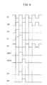
- FIG. 3 is a schematic circuit diagram illustrating a stage in FIG. 2, and FIG. 4 is a timing diagram of signals of the stage in FIG. 3.
- the m-th stage SRCm includes a pull-up section 210 and a pull-down section 220.
- the pull-up section 210 pulls up the m-th gate signal GOUTm to the voltage of the first clock terminal CK1 in response to the carry signal of the (m-1)-th stage SRC(m-1).
- the pull-down section 220 pulls down the m-th gate signal GOUTm to the off-voltage Voff in response to the gate signal GOUT(m+1) of the (m+1)-th stage.
- the pull-up section 210 includes a fifth transistor T5 having a gate electrode connected to a first node N1, a drain electrode connected to the first clock terminal CK1, and a source electrode connected to the output terminal OUT. Therefore, the drain electrode of the fifth transistor T5 receives the first clock signal CK or the second clock signal CKB through the first clock terminal CK1.
- the pull-down section 220 includes a sixth transistor T6 having a gate electrode connected to a second node N2, a drain electrode connected to the output terminal OUT, and a source electrode connected to the voltage terminal V. The off-voltage is provided to the source electrode of the sixth transistor T6.
- the m-th stage further includes a pull-up driving circuit.
- the pull-up driving circuit turns on the pull-up section 210 in response to the carry signal of the (m-1)-th stage SRC(m-1), and turns off the pull-up section 210 in response to the gate signal GOUT(m+1) of the (m+1)-th stage SRC(m+1).
- the pull-up driving circuit includes a buffer section 280, a charging section 270 and a discharging section 230.
- the buffer section 280 includes a thirteenth transistor T13 having a gate electrode connected to the first input terminal IN1, a drain electrode connected to the first input terminal IN1, and a source electrode connected to the first node N1.
- the charging section 270 includes a third capacitor C3 having a first electrode connected to the first node N1 and a second electrode connected to the output terminal OUT.
- the discharging section 230 includes a seventh transistor T7 having a gate electrode connected to the second input terminal IN2, a drain electrode connected to the first node N1, and a source electrode connected to the voltage terminal V. The off-voltage Voff is provided to the source electrode of the seventh transistor T7.
- the carry signal of the (m-1)-th stage SRC(m-1) is applied to the first node N1 to drive the first node N1 to a high voltage, and the carry signal of the (m-1)-th stage charges the third capacitor C3.
- the third capacitor C3 is charged to at least the threshold voltage of the fifth transistor T5 and the first clock terminal CK1 becomes high, the fifth transistor T5 turns on to transfer the high voltage at the first clock terminal CK1 to the output terminal OUT.
- the fifth transistor T5 when the fifth transistor T5 turns on, the fifth transistor T5 outputs the gate-on signal on the output terminal OUT of the m-th stage SRCm. Then, when the seventh transistor T7 is turned on in response to the (m+1)-th gate signal GOUT(m+1), the third capacitor C3 is discharged to the off-voltage Voff of the voltage terminal V, so that the fifth transistor T5 is turned off.
- the m-th stage SRCm further includes a first holding section 242 and a second holding section 244 maintaining the first node N1 at the off-voltage Voff.
- the first holding section 242 includes an eighth transistor T8 having a gate electrode connected to the first clock terminal CK1, a drain electrode connected to the first node N1, and a source electrode connected to the output terminal OUT.
- the second holding section 244 includes a ninth transistor T9 having a gate electrode connected to the second clock terminal CK2, a drain electrode connected to the first input terminal IN1, and a source electrode connected to the first node N1.
- the first and second holding sections 242 and 244 maintain the first node N1 at the off-voltage Voff after the m-th gate signal GOUTm is discharged to the off-voltage Voff by the pull-down section 220.
- the m-th gate signal GOUTm has been discharged to the off-voltage Voff and the eighth transistor T8 turns on in response to the clock signal on the first clock terminal CK1
- the Voff voltage of the m-th gate signal GOUTm is applied to the first node N1 to maintain the first node N1 at the off-voltage Voff.
- the ninth transistor T9 when the ninth transistor T9 is turned on in response to the clock signal on the second clock terminal CK2 opposite in phase to the signal on the first clock terminal CK1, the first input signal, at the off-voltage Voff, is applied to the first node N1, to maintain the first node N1 at the off-voltage Voff.
- each of the first and second holding sections 242 and 244 are sequentially turned on in response to the signals on the respective first and second clock terminals CK1 and CK2, to maintain the first node N1 at the off-voltage Voff.
- the m-th stage SRCm further includes a third holding section 246, a fourth holding section 248, and a switching section 250.
- the third and fourth holding sections 246 and 248 maintain the m-th gate signal GOUTm at the off-voltage Voff.
- the switching section 250 controls on/off switching of the fourth holding section 248.
- the third holding section 246 includes a tenth transistor T10 having a gate electrode connected to the second clock terminal CK2, a drain electrode connected to the output terminal OUT, and a source electrode connected to the voltage terminal V.
- the source electrode of the tenth transistor T10 receives the off-voltage Voff.
- the fourth holding section 248 includes an eleventh transistor T11 having a gate electrode connected to the second node N2 of the switching section 250, a drain electrode connected to the output terminal OUT, and a source electrode connected to the voltage terminal V.
- the source electrode of the eleventh transistor T11 receives the off-voltage Voff.
- the switching section 250 includes first; second, third and fourth transistors T1, T2, T3 and T4, and first and second capacitors C1 and C2.
- the first transistor T1 has a gate electrode connected to the first clock terminal CK1, a drain electrode connected to the first clock terminal CK1, and a source electrode connected to a drain electrode of the second transistor T2.
- the gate and drain electrodes receive the signal on the first clock terminal CK1.
- the second transistor T2 has a gate electrode connected to the output terminal OUT, and a source electrode connected to the voltage terminal V to receive the off-voltage Voff.
- the third transistor T3 has a drain electrode connected to the first clock terminal CK1, a gate electrode connected to the first clock terminal CK1 through the capacitor C1, and a source electrode connected to the second node N2. Therefore, the drain and gate electrodes of the third transistor T3 receive the signal on the first clock terminal CK1.
- the second capacitor C2 is connected between the gate and source electrodes of the third transistor T3.
- the fourth transistor T4 has a gate electrode connected to the output terminal OUT, a drain electrode connected to the second node N2, and a source electrode connected to the voltage terminal V to receive the off-voltage Voff.
- the output terminal OUT is pulled up to a high voltage. Consequently, the second and fourth transistors T2 and T4 are turned on, and the current provided by the first and third transistors T1 and T3 is discharged through the second and fourth transistors T2 and T4. Therefore, the second node N2 is maintained at a low voltage, so that the eleventh transistor T11 is off.
- the eleventh transistor T11 is turned on.
- the tenth transistor T10 is turned on by the voltage on the second clock terminal CK2, which voltage is opposite in phase to the voltage on the first clock terminal CK1, so that the output terminal OUT is discharged to the off-voltage Voff.
- Each of the third and fourth holding sections 246 and 248 sequentially discharges the output terminal OUT to the off-voltage Voff in response the signals on the respective second and first clock terminals CK2 and CK1.
- the m-th stage of the gate driving circuit 200 further includes a reset section 260 and a carry section 290.
- the reset section 260 includes a twelfth transistor T12 having a gate electrode connected to the reset terminal RE, a drain electrode connected to the first node N1, and a source electrode connected to the voltage terminal V to receive the off-voltage Voff.
- the twelfth transistor T12 When the carry signal of the final stage SRC(n+1) is provided to the reset terminal RE, the twelfth transistor T12 is turned on, so that the first node N1 is discharged to the off-voltage Voff. Therefore, the m-th gate signal GOUTm is discharged to the off-voltage Voff by the carry signal of the (n+1)-th stage SRC(n+1).
- the carry section 290 includes a fourteenth transistor T14 having a gate electrode connected to the first node N1, a drain electrode connected to the first clock terminal CK1 (to receive the first clock signal CK for example), and a source electrode connected to the carry terminal CR.
- the carry section 290 passes the high level of the first clock signal CK to the carry terminal CR when the voltage on the first node N1 becomes high.
- the m-stage's first and second holding sections have different electrical characteristics.
- the width-to-length ratio (W/L) of the ninth transistor is larger than the width-to-length ratio (W/L) of the eighth transistor to reduce the ripple at the first node N1.
- FIG. 5 is a schematic circuit diagram illustrating the ripple improvement at the first node according to some embodiments of the present invention.
- a ripple occurs at the first node N1 connected to the control electrode of the pull-up section 210 since the first node N1 is coupled to the first clock terminal CK1 by first, second and third parasitic capacitances Cgd1, Cgd2 and Cgd3 of the pull-up section 210, the first holding section 242 and the carry section 290.
- the ripple is caused by the first clock terminal CK1 being coupled to (a) the first parasitic capacitance Cgd1 between the drain and gate electrodes of the fifth transistor T5, (b) the second parasitic capacitance Cgd2 between the drain and gate electrodes of the eighth transistor T8, and (c) the third parasitic capacitance Cgd3 between the drain and gate electrodes of the fourteenth transistor T14.
- the ripple may turn on the fifth transistor T5 when the transistor is supposed to be off, so that an abnormal gate-on signal occurs on the output terminal OUT to cause a driving defect.
- a rising edge of the first clock signal CK may raise the voltage on the first node N1 to produce an abnormal gate-on signal, so that a driving defect occurs.
- a ripple may be caused at the first node N1 by parasitic capacitance Cgs of the second holding section 244.
- This capacitance Cgs couples the first node N1 to the second clock terminal CK2.
- the parasitic capacitance Cgs is the capacitance between the gate and source electrodes of the ninth transistor T9.
- the ripple caused by the parasitic capacitive coupling with the second clock terminal CK2 (“reverse ripple") has the opposite phase relative to the ripple caused by the parasitic capacitive coupling with the first clock terminal CK1.
- the reverse ripple caused by the parasitic capacitive coupling with the second clock terminal CK2 compensates the ripple caused by the parasitic capacitive coupling with the first clock terminal CK1, to reduce the total ripple at the first node N1.
- the total ripple may be decreased by as much as the difference between the ripple caused by the parasitic capacitances Cgd1, Cgd2 and Cgd3 of the fifth, eighth and fourteenth transistors T5, T8 and T14, and the ripple caused by the parasitic capacitance Cgs of the ninth transistor T9, to decrease the total ripple at the first node N1.
- the ninth transistor T9 has a large width-to-length ratio (W/L) to increase the parasitic capacitance Cgs, the reverse ripple is increased to reduce the total ripple at the first node N1.
- FIG. 6 is a waveform diagram illustrating a simulated ripple at the first node N1 of FIG. 5.
- the first node N1 is supposed to be at an off-voltage of -7 V during "gate-off" time, i.e., when the gate signal GOUT is at the gate-off voltage.
- the first node N1 may be raised to a higher voltage due to a ripple caused by the parasitic capacitances between the first node N1 and the clock terminals.
- the ripple is smaller however if the ninth transistor T9 has the channel width of 900 ⁇ m compared to the channel width of 25 ⁇ m (the channel length is assumed the same for both cases).
- the ripple at the first node may be decreased by increasing the channel width of the ninth transistor T9.
- the ripple at the first node may be decreased in this case also by increasing the channel width of the ninth transistor T9.
- the ninth transistor T9 performs the same function as the thirteenth transistor T13 when the third capacitor C3 is discharged. Therefore, if the width-to-length ratio (W/L) of the ninth transistor T9 is increased, the current-voltage (I-V) characteristics may be improved and the charging rate of the third capacitor C3 by the first input signal may be improved, so that a low temperature driving margin of the fifth transistor T5 may be enhanced.
- W/L width-to-length ratio
- I-V current-voltage
- Table 2 shows results obtained for the low temperature driving margin and a normal temperature frequency driving margin for different width-to-length ratios (W/L) of the ninth transistor T9. The results were obtained for the channel length of the ninth transistor T9 being constant as the channel width of the ninth transistor T9 assumed values of 25 ⁇ m and 936 ⁇ m.
- Conditions Temperature at Driving Defect [°C] Normal Temperature Frequency Driving Margin [Hz] Voltage [V] Width of T9 [ ⁇ m] Cgs:Cgd Min. Max. Min. Max. dV Voff 25 10 -33 -18 115 121 38 -7.4 936 11 -50 -24 124 >130 34 to 38 -7.4
- the ninth transistor T9 may operate at lower voltages (dV) and at lower temperatures (below -20°C), and the normal temperature frequency driving margin increases beyond 124 Hz.
- the ninth transistor T9 has a larger width-to-length ratio (W/L) than the eighth transistor T8.
- W/L width-to-length ratio
- the reverse ripple increases to reduce the total ripple at the first node N1.
- both the ninth transistor T9 and the thirteenth transistor T13 are on, the charging rate of the third capacitor C3 by the first input signal is improved, and hence the low temperature driving margin is enhanced.
- the width-to-length ratio (W/L) of the ninth transistor T9 should preferably be larger than that of the eighth transistor T8 but smaller than the sum of the width-to-length ratios (W/L) of the eighth transistor T8 and the fourteenth transistor T14.
- FIG. 7 is a detailed block diagram illustrating a gate driving circuit of FIG. 1 according to a second example.
- the gate driving circuit of this embodiment is similar to that of the first example.
- the same reference numerals will be used to refer to the same or like parts for the first and second example, and repetitive explanation of such parts will be avoided.
- the gate driving circuit 200 of FIG. 7 includes a circuit section CS and a line section LS.
- the circuit section CS includes first to (n+1)-th stages SRC1 to SRC(n+1) that are cascade-connected to each other, for sequentially outputting the gate-on voltage as the gate signal GOUT.
- the line section LS provides various control signals to the circuit section CS.
- Each of the first to (n+1)-th stages SRC1 to SRC(n+1) includes a first clock terminal CK1, a second clock terminal CK2, a first input terminal IN1, a second input terminal IN2, a voltage terminal V, a reset terminal RE and an output terminal OUT.
- the first and second clock terminals CK1 and CK2 of each of the first to (n+1)-th stages SRC1 to SRC(n+1) receive clock signals of opposite phases.
- a vertical start signal STV is provided to the first input terminal IN1 of the first stage SRC1.
- Gate signals GOUT1 to GOUTn of the respective first to n-th stages SRC1 to SRCn are provided to the first input terminals IN1 of the respective next stages SRC2 to SRC(n+1).
- the gate signals GOUT2 to GOUT(n+1) are provided to the second input terminals IN2 of the respective previous stages SRC1 to SRCn, and the vertical start signal STV is provided to the second input terminal IN2 of the (n+1)-th stage SRC(n+1).
- the gate signal GOUT(n+1) of the (n+1)-th stage SRC(n+1) is provided to the reset terminals RE of the first to (n+1)-th stages SRC1 to SRC(n+1).
- An off-voltage Voff is provided to the voltage terminals V of the first to (n+1)-th stages SRC1 to SRC(n+1).
- Each SRC stage may pass the high level of the clock signal on the first clock terminal CK1 to the output terminal OUT.
- the line section LS includes a start signal line SL1, a first clock signal line SL2, a second clock signal line SL3, a voltage line SL4 and a reset line SL5.
- the vertical start signal STV is provided to the start signal line SL1 from outside, and the start signal line SL1 provides the vertical start signal STV to the first input terminal IN1 of the first stage SRC1 and the second input terminal IN2 of the (n+1)-th stage SRC(n+1).
- the first clock signal line SL2 receives the first clock signal CK
- the second clock signal line SL3 receives the second clock signal CKB opposite in phase to the first clock signal CK.
- the first and second clock signal lines SL2 and SL3 provide the first and second clock signals CK and CKB to the first to (n+1)-th stages SRC1 to SRC(n+1).
- the voltage line SL4 receives the off-voltage Voff, and provides the off-voltage Voff to the voltage terminals of the first to (n+1)-th stages SRC1 to SRC(n+1).
- the reset line SL5 receives the gate signal GOUT(n+1) of the final stage SRC(n+1), and provides the gate signal GOUT(n+1) to the reset terminals RE of the first to (n+1)-th stages SRC1 to SRC(n+1).
- each m-th stage SRCm (m>1) of the gate driving circuit receives the gate signal GOUT(m-1) of the (m-1)-th stage SRC(m-1) as a start signal needed for the operation of the m-th stage SRCm.
- FIG. 8 is a schematic circuit diagram illustrating a single SRC stage of FIG. 7.
- the SRC stage of the present example is similar to that of the first example.
- the same reference numerals will be used to refer to the same or like parts of the first and second examples, and repetitive explanation will be avoided.
- the stage SRCm (1 ⁇ m ⁇ n+1)) includes a pull-up section 210 and a pull-down section 220.
- the pull-up section 210 pulls up the m-th gate signal GOUTm to the voltage of the first clock signal CK (assuming for the sake of illustration that the first clock terminal CK1 receives the first clock signal CK) in response to the (m-1)-th gate signal GOUT(m-1) if m>1.
- the pull-down section 220 pulls down the m-th gate signal GOUTm to the off-voltage Voff in response to the (m+1)-th gate signal GOUT(m+1) if m ⁇ n+1.
- the m-th stage SRCm further includes a pull-up driving circuit.
- the pull-up driving circuit turns on the pull-up section 210 in response to the (m-1)-th gate signal GOUT(m-1), and turns off the pull-up section 210 in response to the (m+1)-th gate signal GOUT(m+1).
- the pull-up driving circuit includes a buffer section 280, a charging section 270 and a discharging section 230.
- the m-th stage SRCm further includes a first holding section 242 and a second holding section 244.
- the first holding section 242 maintains the first node N1 at the off-voltage Voff in response to the first clock signal CK
- the second holding section 244 maintains the first node N1 at the off-voltage Voff in response to the second clock signal CKB.
- the m-th stage SRCm includes third and fourth holding sections 246 and 248 maintaining the m-th gate signal GOUTm at the off-voltage Voff, and a switching section 250 controlling on/off switching of the fourth holding section 248.
- the third holding section 246 controls the on/off switching in response to the second clock signal CKB
- the third and fourth holding sections 246 and 248 alternately discharge the output terminal OUT to the off-voltage Voff.
- the m-th stage SRCm further comprises a reset section 260.
- the reset sections 260 of the first to (n+1)-th stages SRC1 to SRC(n+1) simultaneously discharge the respective first nodes N1 to the off-voltage Voff in response to the (n+1)-th gate signal GOUT(n+1).
- the first holding section 242 and the second holding section 244 have different electrical characteristics.
- the width-to-length ratio (W/L) of the ninth transistor may be made larger than the width-to-length ratio (W/L) of the eighth transistor.
- the reverse ripple at the first node N1, caused by coupling with the second clock signal CKB increases relative to the ripple caused at the first node N1 by coupling with the first clock signal CK, and hence the driving defects are abated.
- the ninth transistor T9 aids the thirteenth transistor T13 when the ninth transistor T9 charges the third capacitor C3, the charging rate of the third capacitor C3 is improved in accordance with the increased width-to-length ratio (W/L) of the ninth transistor T9, so that the low temperature driving margin is enhanced.
- FIG. 9 is a schematic circuit diagram illustrating a stage of a gate driving circuit according to a third example.
- the stage of the present embodiment is substantially the same as in FIG. 2 except for a ninth transistor and a thirteenth transistor.
- the same reference numerals will be used to refer to the same or like parts as those described in FIG. 2 and any repetitive explanation concerning the above elements will be omitted.
- a second holding section 244 includes a ninth transistor T9.
- the ninth transistor T9 includes a gate electrode electrically connected to a second clock terminal CK2, a drain electrode electrically connected to a first input terminal IN1, and a source electrode electrically connected to a first node N1.
- the ninth transistor T9 has an asymmetric structure.
- a parasitic capacitance Cgs between the gate and source electrodes of the ninth transistor T9 is different from a parasitic capacitance Cgd between the gate and drain electrodes of the ninth transistor T9.
- the parasitic capacitance Cgs is greater than the parasitic capacitance Cgd.
- the m-th stage SRCm includes a pull-up driving circuit.
- the pull-up driving circuit turns on the pull-up section 210 in response to a carry signal provided from an (m-1)-th stage SRCm-1, and turns off the pull-up section 210 in response to a gate signal Gm+1 of an (m+1)-th stage SRCm+1.
- the pull-up driving circuit includes a buffer section 280, a charging section 270 and a discharging section 230.
- the buffer section 280 includes a thirteenth transistor T13 having a gate electrode connected to the first input terminal IN1, a drain electrode connected to the first input terminal IN1, and a source electrode connected to the first node N1.
- the carry signal is applied to the first node N1 to raise a voltage level of the first node N1 to charge the third capacitor C3.
- the third capacitor C3 is sufficiently charged to have a higher voltage than the threshold voltage of the fifth transistor T5 and the first clock signal CL is high, the fifth transistor T5 is bootstrapped, so that the first clock signal of a high level is outputted to the output terminal OUT and the m-th gate signal Gm of the m-th stage SRCm is outputted.
- the thirteenth transistor T13 has sufficient channel width, so that when the thirteenth transistor T13 is turned on, the third capacitor C3 electrically connected to the third capacitor C3 is charged enough to enhance driving characteristics.
- the amount of change of the channel width of the thirteenth transistor T13 will be explained in detail.
- FIGS. 10A and 10B are plan views illustrating structures of the ninth transistor in FIG. 9.
- the ninth transistor T9 in FIG. 9 has a channel of an I-shape.
- the ninth transistor T9 includes a gate electrode 111, a channel pattern 113, a plurality of source electrodes 115 and a plurality of drain electrodes 117.
- the channel pattern 113 is disposed on the gate electrode 111.
- a portion of the source electrodes 115 and the drain electrodes 117 is overlapped with the channel pattern 113.
- Each of the source electrodes 115 and the drain electrodes 117 has an I-shape and the source electrodes 115 and the drain electrodes 117 are alternately arranged with each other.
- the source electrodes 115 and the drain electrodes 117 are separated from each other.
- the channel defined by the source electrodes 115 and the drain electrodes 117 has an I-shape with a channel length L and a channel width W.
- the ninth transistor T9 is designed such that a width s of the source electrode 115 is greater than a width d of the drain electrode 117. Therefore, the parasitic capacitance Cgs between the gate electrode 111 and the source electrode 115 becomes greater than the parasitic capacitance Cgd between the gate electrode 111 and the drain electrode 117.
- the ninth transistor T9 in FIG. 9 has a channel with a U-shape.
- the ninth transistor T9 includes a gate electrode 131, a channel pattern 133, a plurality of source electrodes 135 and a plurality of drain electrodes 137.
- the channel pattern 133 is formed on the gate electrode 131.
- the source electrodes 133 and the drain electrodes 137 are formed such that a portion of the source electrodes 133 and the drain electrodes 137 is overlapped with the channel pattern 133.
- Each of the source electrodes 135 has a U-shape, and each of the drain electrodes 137 is inserted into each of the source electrodes 135.
- the channel layer defined by the source electrodes 135 and the drain electrodes 137 has a U-shape with a channel length L and a channel width W.
- the ninth transistor T9 is designed such that the width s of the each of the source electrodes 135 is greater than the width d of each of the drain electrodes 137. Therefore, the parasitic capacitance Cgs between the gate electrode 131 and each of the source electrodes 135 becomes greater than the parasitic capacitance Cgd between the gate electrode 131 and each of the drain electrodes 137.
- a ratio of the parasitic capacitance Cgs between the gate electrode and the source electrode to the parasitic capacitance Cgd between the gate electrode and the drain electrode is K:1 (K >1), for example about 2:1, about 3:1 or about 4:1.
- FIG. 11 is a graph showing simulated voltage ripples at a first node in FIG. 9.
- the graph in FIG. 11 was measured from the first node N1 of the stage adopting the fifth transistor T5 having a channel width W of about 3,500 ⁇ m, the ninth transistor T9 having a channel width W of about 400 ⁇ m, the fifth transistor T5 having the channel length L of about 5 ⁇ m to about 6 ⁇ m, and the ninth transistor T9 having a channel length L that is substantially the same as the fifth transistor T5.
- a first ripple pattern R1 corresponds to the ratio of the parasitic capacitance Cgs between the gate and source electrodes of the ninth transistor T9 to the parasitic capacitance Cgd between the gate and drain electrodes of the ninth transistor T9 is about 1:1.
- a second ripple pattern R2 corresponds to the ratio of the parasitic capacitance Cgs between the gate and source electrodes of the ninth transistor T9 to the parasitic capacitance Cgd between the gate and drain electrodes of the ninth transistor T9 is about 2:1.
- the voltage difference Vgs between the gate and source electrodes of the ninth transistor T9 to the parasitic capacitance Cgd between the gate and drain electrodes of the ninth transistor T9 is raised to about 1.41 V.
- the second ripple pattern R2 when the ratio of the parasitic capacitance Cgs between the gate and source electrodes of the ninth transistor T9 to the parasitic capacitance Cgd between the gate and drain electrodes of the ninth transistor T9 is about 2:1, the voltage difference Vgs between the gate and source electrodes of the fifth transistor T3 in FIG. 3 (or a voltage of the first node N1) is raised to about 1.29 V. That is, a peak of the second ripple pattern R2 is reduced by about 0.12 V in comparison with a peak of the first ripple pattern R1.
- the ratio of the parasitic capacitance Cgs between the gate and source electrodes of the ninth transistor T9 to the parasitic capacitance Cgd between the gate and drain electrodes of the ninth transistor T9 is increased to be about 2:1, the peak of the ripple measured at the first node N1 is decreased.
- Table 3 shows data of transistors in FIG. 9 when the transistors are driven for 3,000 hours.
- the ninth, tenth and eighteenth transistors T9, T10 and T18 which receive the first and second clock signals CK and CKB, are deteriorated due to gate bias stress, so that the threshold voltage Vth is shifted in comparison with other transistors to lower driving ability.
- the ratio of the parasitic capacitance Cgs to the parasitic capacitance Cgd of the transistor T9 is increased not increasing the channel width of the ninth transistor T9, and the channel width of the thirteenth transistor T13, of which a threshold voltage Vth is relatively less shifted, is increased so that the fifth transistor T5 may be sufficiently charged, according to the present invention.
- the thirteenth transistor T13 charges the third capacitor C3 electrically connected to the first node N1 when the thirteenth transistor T13 is turned on as well as the ninth transistor T9.
- the fifth transistor T5 may be charged enough to enhance driving reliability even when the stages are driven for a long time.
- a conventional thirteenth transistor T13 has a channel width of about 1,200 micrometers ( ⁇ m). Therefore, the thirteenth transistor T13 according to the present embodiment has a channel width of no less than about 1,200 ⁇ m within an allowed area limitation.
- the width of the thirteenth transistor T13 is increased as much as an amount ⁇ W T9 , which corresponds to an increased amount of channel of the ninth transistor T9.
- W T9 is a channel width of the ninth transistor T9, when the ratio Cgs to Cgd is about 1:1 (or symmetric).
- the amount ⁇ W T9 corresponds to a reduced amount of the channel width in comparison with W T of the ninth transistor T9 having the ratio Cgs to Cgd is about 1:1, when the Cgd of the ninth transistor T9 is reduced without changing the Cgs such that the ratio Cgs to Cgd is about K:1 (K>1).
- the ripple of the first node N1 may be reduced when the ninth transistor T9 is designed such that the ratio Cgs:Cgd is about 3:1 without changing the channel width of the ninth transistor T9.
- a range of the amount ⁇ W T9 may be expressed as the following Equation 2 in accordance with an equation W T8 ⁇ W T9 ⁇ W T8+ W T14 through which the channel width of the ninth transistor T9 is obtained.
- W T ⁇ 8 ⁇ 1 - 1 / K ⁇ W T ⁇ 9 W T ⁇ 9 ⁇ 1 - 1 / K ⁇ W T ⁇ 8 + W T ⁇ 14 ⁇ ( 1 - 1 / K )
- W T8 is a width of the eighth transistor T8, and W T14 is a width of the fourteenth transistor T14.
- FIG. 12 is a graph illustrating frequency characteristics of a gate driving circuit according to operating time.
- comparative example A employs the ninth transistor T9 of which a ratio of the parasitic capacitance Cgs between the gate and source electrodes to the parasitic capacitance Cgd between the gate and drain electrodes is about 1:2 or about 1:3, and the thirteenth transistor T13, which is substantially the same as the conventional one, having the channel width of about 1,200 ⁇ m.
- Example B according to the present invention employs the ninth transistor T9 of which a ratio of the parasitic capacitance Cgs between the gate and source electrodes to the parasitic capacitance Cgd between the gate and drain electrodes is about 1:2 or about 1:3, and the thirteenth transistor T13 having the channel width of about 1,600 ⁇ m.
- the driving frequency is about 130 Hz at first, but lowered by about 20 Hz after being driven for about 2,000 hours.
- the driving frequency is 130 Hz at first like comparative example A, but lowered by about 10 Hz after being driven for about 2,000 hours.
- Example B has a reduced frequency drop in comparison with comparative example A.
- the width-to-length ratio (W/L) of a transistor in a second holding section is increased, and as a result the reverse ripple increases so that the total ripple occurring at a control electrode of a pull-up section may be decreased. Therefore, generation of an abnormal gate-on signal may be prevented, to reduce driving defects of a display apparatus.
- the width-to-length ratio (W/L) of the transistor in the second holding section is increased, the charging rate of a charging section may be enhanced, so that a low temperature driving margin may be improved.
- a parasitic capacitance between gate and source electrodes of a ninth transistor is increased to reduce a ripple of a first node electrically connected to the source electrode of the ninth transistor.
- a channel width of a thirteenth transistor electrically charging a capacitor connected to the first node is increased to sufficiently charge the capacitor.
- the reliability of the gate driving circuit outputting the gate signal may be enhanced.
Landscapes
- Engineering & Computer Science (AREA)
- Microelectronics & Electronic Packaging (AREA)
- Computer Hardware Design (AREA)
- Chemical & Material Sciences (AREA)
- Crystallography & Structural Chemistry (AREA)
- Physics & Mathematics (AREA)
- Power Engineering (AREA)
- General Physics & Mathematics (AREA)
- Theoretical Computer Science (AREA)
- Control Of Indicators Other Than Cathode Ray Tubes (AREA)
- Shift Register Type Memory (AREA)
- Liquid Crystal (AREA)
- Liquid Crystal Display Device Control (AREA)
Applications Claiming Priority (2)
| Application Number | Priority Date | Filing Date | Title |
|---|---|---|---|
| KR1020060055654A KR101217177B1 (ko) | 2006-06-21 | 2006-06-21 | 게이트 구동회로 및 이를 갖는 표시 장치 |
| KR20070051904A KR101512338B1 (ko) | 2007-05-29 | 2007-05-29 | 게이트 구동회로 및 이를 갖는 표시 장치 |
Publications (3)
| Publication Number | Publication Date |
|---|---|
| EP1870877A2 true EP1870877A2 (fr) | 2007-12-26 |
| EP1870877A3 EP1870877A3 (fr) | 2009-10-07 |
| EP1870877B1 EP1870877B1 (fr) | 2015-04-01 |
Family
ID=38577429
Family Applications (1)
| Application Number | Title | Priority Date | Filing Date |
|---|---|---|---|
| EP07011735.3A Active EP1870877B1 (fr) | 2006-06-21 | 2007-06-15 | Circuit de commande de grille et appareil d'affichage le comportant |
Country Status (3)
| Country | Link |
|---|---|
| US (1) | US7936332B2 (fr) |
| EP (1) | EP1870877B1 (fr) |
| JP (1) | JP5005440B2 (fr) |
Cited By (9)
| Publication number | Priority date | Publication date | Assignee | Title |
|---|---|---|---|---|
| CN103198782B (zh) * | 2013-03-07 | 2016-02-10 | 京东方科技集团股份有限公司 | 移位寄存器、栅极驱动电路及其修复方法和显示装置 |
| US9741309B2 (en) | 2009-01-22 | 2017-08-22 | Semiconductor Energy Laboratory Co., Ltd. | Method for driving display device including first to fourth switches |
| US9825059B2 (en) | 2009-09-10 | 2017-11-21 | Semiconductor Energy Laboratory Co., Ltd. | Semiconductor device and display device |
| US9941308B2 (en) | 2008-11-28 | 2018-04-10 | Semiconductor Energy Laboratory Co., Ltd. | Display device and electronic device including the same |
| US10205452B2 (en) | 2014-09-30 | 2019-02-12 | Semiconductor Energy Laboratory Co., Ltd. | Logic circuit, semiconductor device, electronic component, and electronic device |
| US10741138B2 (en) | 2009-01-16 | 2020-08-11 | Semiconductor Energy Laboratory Co., Ltd. | Liquid crystal display device and electronic device including the same |
| US11127858B2 (en) | 2009-03-27 | 2021-09-21 | Semiconductor Energy Laboratory Co., Ltd. | Semiconductor device |
| US11222906B2 (en) | 2010-02-23 | 2022-01-11 | Semiconductor Energy Laboratory Co., Ltd. | Display device, semiconductor device, and driving method thereof |
| US11545105B2 (en) | 2009-09-16 | 2023-01-03 | Semiconductor Energy Laboratory Co., Ltd. | Semiconductor device and electronic appliance |
Families Citing this family (55)
| Publication number | Priority date | Publication date | Assignee | Title |
|---|---|---|---|---|
| TWI250504B (en) * | 2004-07-02 | 2006-03-01 | Hannstar Display Corp | Pixel structure of a liquid crystal display and driving method thereof |
| JP4932415B2 (ja) | 2006-09-29 | 2012-05-16 | 株式会社半導体エネルギー研究所 | 半導体装置 |
| KR101472513B1 (ko) | 2008-07-08 | 2014-12-16 | 삼성디스플레이 주식회사 | 게이트 드라이버 및 이를 갖는 표시장치 |
| KR20100006063A (ko) * | 2008-07-08 | 2010-01-18 | 삼성전자주식회사 | 게이트 드라이버 및 이를 갖는 표시장치 |
| KR101471553B1 (ko) * | 2008-08-14 | 2014-12-10 | 삼성디스플레이 주식회사 | 게이트 구동 회로 및 이를 갖는 표시 장치 |
| CN102160103B (zh) * | 2008-09-19 | 2013-09-11 | 株式会社半导体能源研究所 | 显示装置 |
| KR101511126B1 (ko) * | 2008-10-30 | 2015-04-13 | 삼성디스플레이 주식회사 | 게이트 구동회로 및 이를 구비한 표시 장치 |
| US8232947B2 (en) | 2008-11-14 | 2012-07-31 | Semiconductor Energy Laboratory Co., Ltd. | Liquid crystal display device |
| KR101544052B1 (ko) * | 2009-02-11 | 2015-08-13 | 삼성디스플레이 주식회사 | 게이트 구동회로 및 이를 구비한 표시 장치 |
| TWI401663B (zh) * | 2009-03-13 | 2013-07-11 | Au Optronics Corp | 具雙向穩壓功能之液晶顯示裝置 |
| US8872751B2 (en) | 2009-03-26 | 2014-10-28 | Semiconductor Energy Laboratory Co., Ltd. | Liquid crystal display device having interconnected transistors and electronic device including the same |
| JP5410521B2 (ja) * | 2009-06-15 | 2014-02-05 | シャープ株式会社 | シフトレジスタおよび表示装置 |
| KR102071057B1 (ko) * | 2009-06-25 | 2020-01-29 | 가부시키가이샤 한도오따이 에네루기 켄큐쇼 | 표시 장치 |
| JP5427495B2 (ja) * | 2009-07-07 | 2014-02-26 | 株式会社ジャパンディスプレイ | ゲート信号線駆動回路及び表示装置 |
| KR101752834B1 (ko) * | 2009-12-29 | 2017-07-03 | 삼성디스플레이 주식회사 | 게이트 구동회로 및 이를 포함하는 표시장치 |
| JP5358465B2 (ja) * | 2010-01-25 | 2013-12-04 | 株式会社ジャパンディスプレイ | 表示装置 |
| WO2011096153A1 (fr) | 2010-02-05 | 2011-08-11 | Semiconductor Energy Laboratory Co., Ltd. | Dispositif d'affichage |
| JP5465029B2 (ja) * | 2010-02-09 | 2014-04-09 | 株式会社ジャパンディスプレイ | 表示装置および電子機器 |
| EP2565877A4 (fr) * | 2010-04-28 | 2013-07-10 | Sharp Kk | Registre à décalage et dispositif d'affichage |
| KR101707935B1 (ko) * | 2010-05-12 | 2017-02-20 | 삼성디스플레이 주식회사 | 표시 장치 |
| CN102254503B (zh) | 2010-05-19 | 2013-06-12 | 北京京东方光电科技有限公司 | 移位寄存器单元、显示器用栅极驱动装置及液晶显示器 |
| TWI416874B (zh) * | 2010-08-13 | 2013-11-21 | Au Optronics Corp | 移位暫存裝置與主動陣列基板 |
| KR20120065788A (ko) | 2010-12-13 | 2012-06-21 | 삼성모바일디스플레이주식회사 | 쉬프트 레지스터 및 표시 장치 |
| JP2012249377A (ja) * | 2011-05-26 | 2012-12-13 | Sanken Electric Co Ltd | ゲート駆動回路 |
| TWI449010B (zh) * | 2011-05-27 | 2014-08-11 | Univ Nat Chiao Tung | Display device of the drive circuit |
| KR101861350B1 (ko) * | 2011-07-29 | 2018-05-29 | 삼성디스플레이 주식회사 | 게이트 구동회로 및 이를 포함하는 표시 장치 |
| CN102629444B (zh) * | 2011-08-22 | 2014-06-25 | 北京京东方光电科技有限公司 | 栅极集成驱动电路、移位寄存器及显示屏 |
| CN102629459A (zh) * | 2011-10-26 | 2012-08-08 | 北京京东方光电科技有限公司 | 栅线驱动方法、移位寄存器及栅线驱动装置 |
| CN202443728U (zh) * | 2012-03-05 | 2012-09-19 | 京东方科技集团股份有限公司 | 移位寄存器、栅极驱动器及显示装置 |
| CN202677790U (zh) * | 2012-04-13 | 2013-01-16 | 京东方科技集团股份有限公司 | 移位寄存器单元、移位寄存器和显示装置 |
| CN102819998B (zh) * | 2012-07-30 | 2015-01-14 | 京东方科技集团股份有限公司 | 移位寄存器和显示装置 |
| CN102867475A (zh) * | 2012-09-13 | 2013-01-09 | 京东方科技集团股份有限公司 | 移位寄存器单元、栅极驱动电路及显示装置 |
| CN103000151B (zh) * | 2012-11-29 | 2014-09-10 | 京东方科技集团股份有限公司 | 一种栅极驱动装置及显示设备 |
| CN103198781B (zh) * | 2013-03-01 | 2015-04-29 | 合肥京东方光电科技有限公司 | 移位寄存器单元、栅极驱动装置及显示装置 |
| KR102028992B1 (ko) * | 2013-06-27 | 2019-10-07 | 엘지디스플레이 주식회사 | 쉬프트 레지스터 |
| CN103714780B (zh) | 2013-12-24 | 2015-07-15 | 京东方科技集团股份有限公司 | 栅极驱动电路、方法、阵列基板行驱动电路和显示装置 |
| CN103730089B (zh) | 2013-12-26 | 2015-11-25 | 京东方科技集团股份有限公司 | 栅极驱动电路、方法、阵列基板行驱动电路和显示装置 |
| CN104183219B (zh) * | 2013-12-30 | 2017-02-15 | 昆山工研院新型平板显示技术中心有限公司 | 扫描驱动电路和有机发光显示器 |
| CN103714781B (zh) * | 2013-12-30 | 2016-03-30 | 京东方科技集团股份有限公司 | 栅极驱动电路、方法、阵列基板行驱动电路和显示装置 |
| CN103778896B (zh) | 2014-01-20 | 2016-05-04 | 深圳市华星光电技术有限公司 | 集成栅极驱动电路及具有集成栅极驱动电路的显示面板 |
| US9557840B2 (en) * | 2014-02-04 | 2017-01-31 | Apple Inc. | Displays with intra-frame pause |
| CN104090436B (zh) * | 2014-06-26 | 2017-03-22 | 京东方科技集团股份有限公司 | 一种阵列基板的栅极行驱动电路及显示装置 |
| KR20160021942A (ko) * | 2014-08-18 | 2016-02-29 | 삼성디스플레이 주식회사 | 표시 장치 및 이의 구동 방법 |
| CN104376824A (zh) * | 2014-11-13 | 2015-02-25 | 深圳市华星光电技术有限公司 | 用于液晶显示的goa电路及液晶显示装置 |
| CN104517575B (zh) * | 2014-12-15 | 2017-04-12 | 深圳市华星光电技术有限公司 | 移位寄存器及级传栅极驱动电路 |
| KR20160103616A (ko) * | 2015-02-24 | 2016-09-02 | 삼성디스플레이 주식회사 | 주사 구동부 |
| CN104809978B (zh) | 2015-05-21 | 2017-05-17 | 京东方科技集团股份有限公司 | 移位寄存器单元、驱动方法、栅极驱动电路及显示装置 |
| CN104835442B (zh) * | 2015-05-28 | 2017-09-26 | 京东方科技集团股份有限公司 | 移位寄存器及其驱动方法、栅极驱动电路和显示装置 |
| CN106297704B (zh) * | 2016-08-31 | 2019-06-11 | 深圳市华星光电技术有限公司 | 一种栅极驱动电路 |
| CN206470511U (zh) * | 2017-02-24 | 2017-09-05 | 中华映管股份有限公司 | 液晶显示器 |
| CN108492791B (zh) * | 2018-03-26 | 2019-10-11 | 京东方科技集团股份有限公司 | 一种显示驱动电路及其控制方法、显示装置 |
| CN209132559U (zh) * | 2019-01-09 | 2019-07-19 | 北京京东方技术开发有限公司 | 一种显示基板、显示装置 |
| KR102877191B1 (ko) * | 2021-11-04 | 2025-10-28 | 엘지디스플레이 주식회사 | 게이트 구동 회로 및 표시 장치 |
| CN115547269B (zh) * | 2022-10-10 | 2025-11-28 | Tcl华星光电技术有限公司 | 栅极驱动电路及显示面板 |
| CN116798497A (zh) * | 2023-06-19 | 2023-09-22 | 合肥京东方卓印科技有限公司 | 一种移位寄存器单元、栅极驱动电路及显示装置 |
Family Cites Families (12)
| Publication number | Priority date | Publication date | Assignee | Title |
|---|---|---|---|---|
| US6611248B2 (en) * | 2000-05-31 | 2003-08-26 | Casio Computer Co., Ltd. | Shift register and electronic apparatus |
| TW525139B (en) * | 2001-02-13 | 2003-03-21 | Samsung Electronics Co Ltd | Shift register, liquid crystal display using the same and method for driving gate line and data line blocks thereof |
| JP4302535B2 (ja) * | 2002-04-08 | 2009-07-29 | サムスン エレクトロニクス カンパニー リミテッド | ゲート駆動回路及びこれを有する液晶表示装置 |
| KR100797522B1 (ko) * | 2002-09-05 | 2008-01-24 | 삼성전자주식회사 | 쉬프트 레지스터와 이를 구비하는 액정 표시 장치 |
| US7319452B2 (en) * | 2003-03-25 | 2008-01-15 | Samsung Electronics Co., Ltd. | Shift register and display device having the same |
| US7486269B2 (en) * | 2003-07-09 | 2009-02-03 | Samsung Electronics Co., Ltd. | Shift register, scan driving circuit and display apparatus having the same |
| KR100705628B1 (ko) * | 2003-12-30 | 2007-04-11 | 비오이 하이디스 테크놀로지 주식회사 | 액정표시장치의 구동회로 |
| US7289594B2 (en) * | 2004-03-31 | 2007-10-30 | Lg.Philips Lcd Co., Ltd. | Shift registrer and driving method thereof |
| KR101026807B1 (ko) | 2004-06-09 | 2011-04-04 | 삼성전자주식회사 | 표시 장치용 구동 장치 및 표시판 |
| TWI382264B (zh) * | 2004-07-27 | 2013-01-11 | Samsung Display Co Ltd | 薄膜電晶體陣列面板及包括此面板之顯示器裝置 |
| KR101061846B1 (ko) * | 2004-08-19 | 2011-09-02 | 삼성전자주식회사 | 표시 장치용 구동 장치 |
| US7332936B2 (en) * | 2004-12-03 | 2008-02-19 | Semiconductor Energy Laboratory Co., Ltd. | Semiconductor circuit, display device, electronic apparatus |
-
2007
- 2007-06-14 US US11/763,144 patent/US7936332B2/en active Active
- 2007-06-15 EP EP07011735.3A patent/EP1870877B1/fr active Active
- 2007-06-20 JP JP2007162598A patent/JP5005440B2/ja active Active
Cited By (39)
| Publication number | Priority date | Publication date | Assignee | Title |
|---|---|---|---|---|
| US10629134B2 (en) | 2008-11-28 | 2020-04-21 | Semiconductor Energy Laboratory Co., Ltd. | Display device and electronic device including the same |
| US12131706B2 (en) | 2008-11-28 | 2024-10-29 | Semiconductor Energy Laboratory Co., Ltd. | Display device and electronic device including the same |
| US12046203B2 (en) | 2008-11-28 | 2024-07-23 | Semiconductor Energy Laboratory Co., Ltd. | Display device and electronic device including the same |
| US11776483B2 (en) | 2008-11-28 | 2023-10-03 | Semiconductor Energy Laboratory Co., Ltd. | Display device and electronic device including the same |
| US11527208B2 (en) | 2008-11-28 | 2022-12-13 | Semiconductor Energy Laboratory Co., Ltd. | Display device and electronic device including the same |
| US9941308B2 (en) | 2008-11-28 | 2018-04-10 | Semiconductor Energy Laboratory Co., Ltd. | Display device and electronic device including the same |
| US10008519B1 (en) | 2008-11-28 | 2018-06-26 | Semiconductor Energy Laboratory Co., Ltd. | Display device and electronic device including the same |
| US11250785B2 (en) | 2008-11-28 | 2022-02-15 | Semiconductor Energy Laboratory Co., Ltd. | Display device and electronic device including the same |
| US10971075B2 (en) | 2008-11-28 | 2021-04-06 | Semiconductor Energy Laboratory Co., Ltd. | Display device and electronic device including the same |
| US10304873B2 (en) | 2008-11-28 | 2019-05-28 | Semiconductor Energy Laboratory Co., Ltd. | Display device and electronic device including the same |
| US11151953B2 (en) | 2009-01-16 | 2021-10-19 | Semiconductor Energy Laboratory Co., Ltd. | Liquid crystal display device and electronic device including the same |
| US11468857B2 (en) | 2009-01-16 | 2022-10-11 | Semiconductor Energy Laboratory Co., Ltd. | Liquid crystal display device and electronic device including the same |
| US10741138B2 (en) | 2009-01-16 | 2020-08-11 | Semiconductor Energy Laboratory Co., Ltd. | Liquid crystal display device and electronic device including the same |
| US12027133B2 (en) | 2009-01-16 | 2024-07-02 | Semiconductor Energy Laboratory Co., Ltd. | Liquid crystal display device and electronic device including the same |
| US11735133B2 (en) | 2009-01-16 | 2023-08-22 | Semiconductor Energy Laboratory Co., Ltd. | Liquid crystal display device and electronic device including the same |
| US12062310B2 (en) | 2009-01-22 | 2024-08-13 | Semiconductor Energy Laboratory Co., Ltd. | Method for driving display device |
| US10878736B2 (en) | 2009-01-22 | 2020-12-29 | Semiconductor Energy Laboratory Co., Ltd. | Method for driving display device |
| US10896633B2 (en) | 2009-01-22 | 2021-01-19 | Semiconductor Energy Laboratory Co., Ltd. | Method for driving display device |
| US9741309B2 (en) | 2009-01-22 | 2017-08-22 | Semiconductor Energy Laboratory Co., Ltd. | Method for driving display device including first to fourth switches |
| US11551596B2 (en) | 2009-01-22 | 2023-01-10 | Semiconductor Energy Laboratory Co., Ltd. | Method for driving display device |
| US11575049B2 (en) | 2009-03-27 | 2023-02-07 | Semiconductor Energy Laboratory Co., Ltd. | Semiconductor device |
| US11916150B2 (en) | 2009-03-27 | 2024-02-27 | Semiconductor Energy Laboratory Co., Ltd. | Semiconductor device |
| US12294031B2 (en) | 2009-03-27 | 2025-05-06 | Semiconductor Energy Laboratory Co., Ltd. | Semiconductor device |
| US11127858B2 (en) | 2009-03-27 | 2021-09-21 | Semiconductor Energy Laboratory Co., Ltd. | Semiconductor device |
| US10622382B2 (en) | 2009-09-10 | 2020-04-14 | Semiconductor Energy Laboratory Co., Ltd. | Semiconductor device and display device |
| US10269833B2 (en) | 2009-09-10 | 2019-04-23 | Semiconductor Energy Laboratory Co., Ltd. | Semiconductor device and display device |
| US12520589B2 (en) | 2009-09-10 | 2026-01-06 | Semiconductor Energy Laboratory Co., Ltd. | Semiconductor device and display device |
| US12490518B2 (en) | 2009-09-10 | 2025-12-02 | Semiconductor Energy Laboratory Co., Ltd. | Semiconductor device and display device |
| US9825059B2 (en) | 2009-09-10 | 2017-11-21 | Semiconductor Energy Laboratory Co., Ltd. | Semiconductor device and display device |
| US9847352B2 (en) | 2009-09-10 | 2017-12-19 | Semiconductor Energy Laboratory Co., Ltd. | Semiconductor device and display device |
| US10665612B2 (en) | 2009-09-10 | 2020-05-26 | Semiconductor Energy Laboratory Co., Ltd. | Semiconductor device and display device |
| US11545105B2 (en) | 2009-09-16 | 2023-01-03 | Semiconductor Energy Laboratory Co., Ltd. | Semiconductor device and electronic appliance |
| US11984093B2 (en) | 2009-09-16 | 2024-05-14 | Semiconductor Energy Laboratory Co., Ltd. | Semiconductor device and electronic appliance |
| US12400617B2 (en) | 2009-09-16 | 2025-08-26 | Semiconductor Energy Laboratory Co., Ltd. | Semiconductor device and electronic appliance |
| US11222906B2 (en) | 2010-02-23 | 2022-01-11 | Semiconductor Energy Laboratory Co., Ltd. | Display device, semiconductor device, and driving method thereof |
| US11749685B2 (en) | 2010-02-23 | 2023-09-05 | Semiconductor Energy Laboratory Co., Ltd. | Display device, semiconductor device, and driving method thereof |
| US9384686B2 (en) | 2013-03-07 | 2016-07-05 | Boe Technology Group Co., Ltd | Shift register, gate driving circuit and repairing method therefor, and display device |
| CN103198782B (zh) * | 2013-03-07 | 2016-02-10 | 京东方科技集团股份有限公司 | 移位寄存器、栅极驱动电路及其修复方法和显示装置 |
| US10205452B2 (en) | 2014-09-30 | 2019-02-12 | Semiconductor Energy Laboratory Co., Ltd. | Logic circuit, semiconductor device, electronic component, and electronic device |
Also Published As
| Publication number | Publication date |
|---|---|
| JP5005440B2 (ja) | 2012-08-22 |
| JP2008003602A (ja) | 2008-01-10 |
| US7936332B2 (en) | 2011-05-03 |
| EP1870877B1 (fr) | 2015-04-01 |
| EP1870877A3 (fr) | 2009-10-07 |
| US20070296662A1 (en) | 2007-12-27 |
Similar Documents
| Publication | Publication Date | Title |
|---|---|---|
| EP1870877B1 (fr) | Circuit de commande de grille et appareil d'affichage le comportant | |
| CN101093647B (zh) | 栅极驱动电路及具有该栅极驱动电路的显示装置 | |
| US8228282B2 (en) | Gate driving circuit, display apparatus having the same, and method thereof | |
| US8754674B2 (en) | Gate drive circuit and method of driving the same | |
| US8264443B2 (en) | Ripple preventing gate driving circuit and display apparatus having the same | |
| US8957882B2 (en) | Gate drive circuit and display apparatus having the same | |
| US8456409B2 (en) | Gate drive circuit and display apparatus having the same | |
| US9412315B2 (en) | Gate driving circuit and display apparatus having the same | |
| US8174478B2 (en) | Gate driving circuit and display apparatus having the same | |
| US7417458B2 (en) | Gate driving circuit and display apparatus having the same | |
| US8098227B2 (en) | Gate driving circuit and display apparatus having the same | |
| KR101710661B1 (ko) | 게이트 구동회로 및 이를 갖는 표시장치 | |
| US9203395B2 (en) | Gate driver and a display device including the same | |
| US7724864B2 (en) | Shift register and display device having the same | |
| US7880503B2 (en) | Method of driving gate lines, gate line drive circuit for performing the method and display device having the gate line drive circuit | |
| US20100156474A1 (en) | Gate drive circuit and display apparatus having the same | |
| US8610655B2 (en) | Method for removing noise, switching circuit for performing the same and display device having the switching circuit | |
| US8619070B2 (en) | Gate drive circuit and display apparatus having the same | |
| EP2086011A2 (fr) | Transistor de film mince et dispositif d'affichage l'utilisant | |
| KR101512338B1 (ko) | 게이트 구동회로 및 이를 갖는 표시 장치 | |
| KR20080000205A (ko) | 게이트 구동회로 및 이를 포함하는 표시 장치 | |
| KR20070095585A (ko) | 게이트 구동회로 및 이를 갖는 표시 장치 |
Legal Events
| Date | Code | Title | Description |
|---|---|---|---|
| PUAI | Public reference made under article 153(3) epc to a published international application that has entered the european phase |
Free format text: ORIGINAL CODE: 0009012 |
|
| AK | Designated contracting states |
Kind code of ref document: A2 Designated state(s): AT BE BG CH CY CZ DE DK EE ES FI FR GB GR HU IE IS IT LI LT LU LV MC MT NL PL PT RO SE SI SK TR |
|
| AX | Request for extension of the european patent |
Extension state: AL BA HR MK YU |
|
| PUAL | Search report despatched |
Free format text: ORIGINAL CODE: 0009013 |
|
| AK | Designated contracting states |
Kind code of ref document: A3 Designated state(s): AT BE BG CH CY CZ DE DK EE ES FI FR GB GR HU IE IS IT LI LT LU LV MC MT NL PL PT RO SE SI SK TR |
|
| AX | Request for extension of the european patent |
Extension state: AL BA HR MK RS |
|
| 17P | Request for examination filed |
Effective date: 20100329 |
|
| AKX | Designation fees paid |
Designated state(s): DE FR GB IT |
|
| 17Q | First examination report despatched |
Effective date: 20100622 |
|
| RAP1 | Party data changed (applicant data changed or rights of an application transferred) |
Owner name: SAMSUNG ELECTRONICS CO., LTD. |
|
| RAP1 | Party data changed (applicant data changed or rights of an application transferred) |
Owner name: SAMSUNG DISPLAY CO., LTD. |
|
| GRAP | Despatch of communication of intention to grant a patent |
Free format text: ORIGINAL CODE: EPIDOSNIGR1 |
|
| INTG | Intention to grant announced |
Effective date: 20141014 |
|
| GRAS | Grant fee paid |
Free format text: ORIGINAL CODE: EPIDOSNIGR3 |
|
| GRAA | (expected) grant |
Free format text: ORIGINAL CODE: 0009210 |
|
| AK | Designated contracting states |
Kind code of ref document: B1 Designated state(s): DE FR GB IT |
|
| REG | Reference to a national code |
Ref country code: GB Ref legal event code: FG4D |
|
| REG | Reference to a national code |
Ref country code: DE Ref legal event code: R096 Ref document number: 602007040851 Country of ref document: DE Effective date: 20150507 |
|
| RAP2 | Party data changed (patent owner data changed or rights of a patent transferred) |
Owner name: SAMSUNG DISPLAY CO., LTD. |
|
| REG | Reference to a national code |
Ref country code: DE Ref legal event code: R097 Ref document number: 602007040851 Country of ref document: DE |
|
| PLBE | No opposition filed within time limit |
Free format text: ORIGINAL CODE: 0009261 |
|
| STAA | Information on the status of an ep patent application or granted ep patent |
Free format text: STATUS: NO OPPOSITION FILED WITHIN TIME LIMIT |
|
| 26N | No opposition filed |
Effective date: 20160105 |
|
| REG | Reference to a national code |
Ref country code: FR Ref legal event code: PLFP Year of fee payment: 10 |
|
| REG | Reference to a national code |
Ref country code: FR Ref legal event code: PLFP Year of fee payment: 11 |
|
| REG | Reference to a national code |
Ref country code: FR Ref legal event code: PLFP Year of fee payment: 12 |
|
| P01 | Opt-out of the competence of the unified patent court (upc) registered |
Effective date: 20230515 |
|
| PGFP | Annual fee paid to national office [announced via postgrant information from national office to epo] |
Ref country code: DE Payment date: 20250520 Year of fee payment: 19 |
|
| PGFP | Annual fee paid to national office [announced via postgrant information from national office to epo] |
Ref country code: GB Payment date: 20250520 Year of fee payment: 19 |
|
| PGFP | Annual fee paid to national office [announced via postgrant information from national office to epo] |
Ref country code: IT Payment date: 20250523 Year of fee payment: 19 |
|
| PGFP | Annual fee paid to national office [announced via postgrant information from national office to epo] |
Ref country code: FR Payment date: 20250521 Year of fee payment: 19 |