EP1870947A2 - Dispositif de commande pour actionneur piézoélectrique - Google Patents
Dispositif de commande pour actionneur piézoélectrique Download PDFInfo
- Publication number
- EP1870947A2 EP1870947A2 EP07011623A EP07011623A EP1870947A2 EP 1870947 A2 EP1870947 A2 EP 1870947A2 EP 07011623 A EP07011623 A EP 07011623A EP 07011623 A EP07011623 A EP 07011623A EP 1870947 A2 EP1870947 A2 EP 1870947A2
- Authority
- EP
- European Patent Office
- Prior art keywords
- charging
- charging switch
- switch
- signal
- period
- Prior art date
- Legal status (The legal status is an assumption and is not a legal conclusion. Google has not performed a legal analysis and makes no representation as to the accuracy of the status listed.)
- Granted
Links
Images




Classifications
-
- H—ELECTRICITY
- H02—GENERATION; CONVERSION OR DISTRIBUTION OF ELECTRIC POWER
- H02N—ELECTRIC MACHINES NOT OTHERWISE PROVIDED FOR
- H02N2/00—Electric machines in general using piezoelectric effect, electrostriction or magnetostriction
- H02N2/02—Electric machines in general using piezoelectric effect, electrostriction or magnetostriction producing linear motion, e.g. actuators; Linear positioners ; Linear motors
- H02N2/06—Drive circuits; Control arrangements or methods
- H02N2/065—Large signal circuits, e.g. final stages
- H02N2/067—Large signal circuits, e.g. final stages generating drive pulses
-
- F—MECHANICAL ENGINEERING; LIGHTING; HEATING; WEAPONS; BLASTING
- F02—COMBUSTION ENGINES; HOT-GAS OR COMBUSTION-PRODUCT ENGINE PLANTS
- F02D—CONTROLLING COMBUSTION ENGINES
- F02D41/00—Electrical control of supply of combustible mixture or its constituents
- F02D41/20—Output circuits, e.g. for controlling currents in command coils
- F02D41/2096—Output circuits, e.g. for controlling currents in command coils for controlling piezoelectric injectors
Definitions
- the present invention relates to a driving device for charging and discharging a piezoelectric actuator to expand and contract the piezoelectric actuator.
- a conventional driving device for charging and discharging a piezoelectric actuator to expand and contract the piezoelectric actuator includes a charging circuit and a discharging circuit, as disclosed in JP 2005-16431A for example.
- the charging circuit electric power is supplied from a DC power source through a charging switch having MOSFET to a series circuit of an inductor and the piezoelectric actuator.
- the discharging circuit is connected to the series circuit in parallel.
- electric charges charged in the piezoelectric actuator are discharged through a discharging switch having MOSFET.
- the charging switch when a driving signal is input from an external device to the driving device, the charging switch is repetitively turned on/off while the discharging switch is in the turned-off state, thereby charging the piezoelectric actuator and thus expanding the piezoelectric actuator. Then, when no driving signal is input, the discharging switch is repetitively turned on/off while the charging switch is in the turned-off state, thereby discharging the piezoelectric actuator and thus contracting the piezoelectric actuator.
- the piezoelectric actuator is charged in stepwise manner according to the following procedure. That is, the charging switch is turned on while the discharging switch is turned off, whereby charging current flows from the DC power source through the charging circuit into the piezoelectric actuator. Thereafter, the charging switch is turned off so that the charging current (flywheel current) flowing by means of the energy accumulated in an inductor is made to flow from the negative side of the piezoelectric actuator to the positive side thereof through a parasitic diode of MOSFET used as the discharging switch.
- the piezoelectric actuator is discharged in stepwise manner according to the following procedure. That is, the discharging switch is turned on while the charging switch is turned off to make the discharging current flow from the positive side of the piezoelectric actuator to the discharging circuit. Thereafter, the discharging switch is turned off so that charging power is regenerated to the DC power source by a flyback voltage generated by the energy accumulated in the inductor.
- a desired charge amount is charged into the piezoelectric actuator by controlling the amount of charges per unit time which are supplied from the DC power source.
- the charging switch is turned on, and then turned off at the time point when the integration value of the charging current flowing into the piezoelectric actuator reaches a predetermined target value. Thereafter, the charging switch is turned on when the charging current reaches a smaller predetermined value than the target value concerned. This turn-on/off operation is repeated, thereby charging the piezoelectric actuator.
- the current amount of charging current flowing into the piezoelectric actuator at the charging time varies in accordance with surrounding conditions under which the piezoelectric actuator is used.
- the electrostatic capacitance of the piezoelectric actuator When the electrostatic capacitance of the piezoelectric actuator is varied, the amount of current flowing from the DC power source into the piezoelectric actuator when the charging switch is turned on is varied, and thus the energy accumulated in the inductor at that time also varies. Therefore, the time required until the discharging of the energy from the inductor is completed under the state that the charging switch is turned off is also varied.
- the timing at which the charging switch is turned on is varied in accordance with the variation of the electrostatic capacitance of the piezoelectric actuator, and thus the variation amount of charges accumulated in the piezoelectric actuator (that is, the expansion rate at which the piezoelectric actuator expands per unit time) is varied in some cases.
- the conventional driving device is used to control the fuel injection of an injector so that fuel injection is started at the time when the piezoelectric actuator expands by a predetermined amount, the timing of the fuel injection of the injector is varied, and thus it is impossible to perform high-precision fuel injection.
- the present invention therefore has an object to provide a driving device for a piezoelectric actuator that reduces variation of the expansion rate of a piezoelectric actuator due to variation of an electrostatic capacitance.
- a driving device for a piezoelectric actuator has: an inductor connected to the piezoelectric actuator in series so that an inductor and the piezoelectric actuator forms a series circuit; a charging circuit for supplying power from a DC power source through a charging switch to the series circuit; and a discharging circuit that is connected to the series circuit in parallel and discharging charges charged in the piezoelectric actuator through a discharging switch.
- a charge/discharge control unit When a driving instruction is input from an external device, a charge/discharge control unit repeats the turn-on/off operation of the charging switch under the state that the discharging switch is turned off, thereby charging and expanding the piezoelectric actuator. Thereafter, when a driving stop instruction is input from the external device, the charge/discharge control unit repeats the turn-on/off operation of the discharging switch under the state that the charging switch is turned off, thereby discharging and contracting the piezoelectric actuator.
- the charge/discharge control unit includes a target value setting section, a current detecting section, an estimating section and a charging switch driving section.
- the target value setting section sets a target value of charge energy to be charged in the piezoelectric actuator during ON-period of the charging switch on the basis of the charge energy to be charged in the piezoelectric actuator during one charging period by the driving device, and a power supply voltage of the DC power source.
- the charging switch driving section When the driving instruction is input, the charging switch driving section turns on the charging switch at a preset period, and turns off the charging switch every time an estimation value estimated by the estimating section reaches the target value set by the target value setting section.
- the period when the charging switch driving section turns on the charging switch, and the charging amount of the piezoelectric actuator in one turn-on operation of the charging switch can be fixed. Therefore, the expansion rate of the piezoelectric actuator in the charging period can be set to a desired expansion rate.
- the expansion rate of the piezoelectric actuator can be prevented from being varied.
- the driving device is applied to fuel injection control for a fuel injector that starts the fuel injection at the time when the piezoelectric actuator expands by a predetermined amount, the variation of the fuel injection timing of the injector is reduced even when the electrostatic capacitance varies.
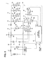
- a driving device 1 is designed to charge/discharge four piezoelectric actuators P1 to P4 mounted in fuel injectors for injecting fuel in an internal combustion engine of a vehicle by expanding/contracting the piezoelectric actuators, thereby making each fuel injector provided on each cylinder of the engine start/stop the fuel injection.
- the driving device 1 includes an inductor L1 that is connected in series to a parallel circuit 10 having the four piezoelectric actuators P1 to P4 connected to one another in parallel, a power supply circuit 12 for boosting a battery voltage from a storage battery 14 to generate a power supply voltage, a charging circuit 30 supplying electric power from the power supply circuit 12 through a charging switch SW1 to a series circuit 20 having the inductor L1 and the parallel circuit 10, a discharging circuit 40 that is connected to the series circuit in parallel to discharge charges charged in the piezoelectric actuators P1 to P4 through a discharging switch SW2, a current detecting resistor R1 for detecting current supplied from the power supply circuit 12 to the piezoelectric actuators P1 to P4 at the charging time, and a switch controller 50 for controlling the turn-on/off operations of the charging switch SW1 and the discharging switch SW2.
- the parallel circuit 10 includes a first series circuit having the piezoelectric actuator P1 and a cylinder selecting switch SWa, a second series circuit having the piezoelectric actuator P2 and a cylinder selecting switch SWb, a third series circuit having the piezoelectric actuator P3 and a cylinder selecting switch SWc, and a fourth series circuit having the piezoelectric actuator P4 and a cylinder selecting switch SWd. These series circuits are connected to one another in parallel.
- One end portion of the parallel circuit 10 at the piezoelectric actuator (P1 to P4) side is connected to one end of the inductor L1, and the other end portion of the parallel circuit 10 at the cylinder selecting switch (SWa to SWd) side is connected to a ground line which is connected to the negative-side of the power supply circuit 12.
- Each of the cylinder selecting switches SWa to SWd is an n-channel MOSFET.
- the source of each n-channel MOSFET is connected to the ground line, the drain thereof is connected to one end of the corresponding piezoelectric actuator (P1 to P4), and the gate thereof is connected to an output terminal of the switch controller 50.
- a diode Da is connected to the cylinder selecting switch SWa in parallel
- a diode Db is connected to the cylinder selecting switch SWb in parallel
- a diode Dc is connected to the cylinder selecting switch SWc in parallel
- a diode Dd is connected to the cylinder selecting switch SWd in parallel.
- each of the diodes Da to Dd is connected to the ground line, and the cathode thereof is connected to the connection point between each piezoelectric actuator (P1 to P4) and the drain of each cylinder selecting switch (SWa to SWd).
- the parasitic diodes of the MOSFETs may be used as the diodes Da to Dd.
- the charging switch SW1 is an n-channel MOSFET.
- the source of the n-channel MOSFET is connected to one end of the inductor L1, the drain thereof is connected to the positive-side of the power supply circuit 12, and the gate thereof is connected to an output terminal of the switch controller 50.
- a diode D1 is connected to the charging switch SW1 in parallel, and the diode D1 serves to allow regenerated current to flow into the power supply circuit 12, when the discharging switch SW2 is turned off at the discharging time of the piezoelectric actuators P1 to P4.
- MOSFET MOSFET
- the parasitic diode of the MOSFET may be used as the diode D1.
- the charging switch SW2 is an n-channel MOSFET.
- the source of the n-channel MOSFET is connected to the ground line, the drain thereof is connected to the connection point between the charging switch SW1 and the inductor L1, and the gate thereof is connected to an output terminal of the switch controller 50.
- a diode D2 is connected to the discharging switch SW2 in parallel, and the diode D2 serves to allow flywheel current to flow, when the charging switch SW1 is turned off at the charging time of the piezoelectric actuators P1 to P4.
- the parasitic diode of the MOSFET may be used as the diode D2.
- the power supply circuit 12 has a boosting circuit 16 for boosting the battery voltage (for example, 12V) from the battery 14.
- the negative-side terminal of the battery 14 is connected to the ground line.
- the boosting circuit 16 has a boosting inductor L2 whose one end is connected to the positive-side terminal of the battery 14, a diode D3 whose anode is connected to the other end of the boosting inductor L2 and whose cathode is connected to the drain of the charging switch SW1, a boosting switch SW3 which is connected to the connection point between the diode D3 and the boosting inductor L2 at one end thereof and also connected to the ground line at the other end thereof, a boosting control circuit 18 for turning on/off the boosting switch SW3, and a buffer capacitor C1 which is connected to the connection point between the diode D3 and the charging switch SW1 at one end thereof and also connected to the ground line through the current detecting resistor R1 at the other end thereof.
- the diode D3 is used to prevent discharge of the buffer capacitor C1.
- the boosting control circuit 18 repetitively turns on/off the boosting switch SW3 to charge a voltage of several tens to several hundreds volts into the buffer capacitor C1 through the diode D3.
- the boosting control circuit 18 is designed to detect the voltage value V of the buffer capacitor C1, and outputs a voltage value signal S representing the voltage value V to the switch controller 50.
- the buffer capacitor C1 makes current flow into the charging circuit 30 to charge the piezoelectric actuator (P1 to P4) corresponding to the turned-on cylinder selecting switch (SWa to SWd).
- the current flowing from the buffer capacitor C1 into the series circuit 20 when the piezoelectric actuator P1 to P4 is charged is called as a buffer capacitor current Ic1.
- the buffer capacitor C1 is designed to have a relatively large electrostatic capacitance, and it keeps a substantially fixed voltage value when power is supplied to the piezoelectric actuators P1 to P4.
- the switch controller 50 When a driving signal Sd output from an external ECU (not shown) for performing the engine control of the vehicle is input to the switch controller 50, the switch controller 50 turns on the cylinder selecting switch SWa to SWd which is specified by the driving signal Sd, and also repetitively turns on/off the charging switch SW1 for a predetermined time under the state that the discharging switch SW2 is turned off.
- the switch controller 50 periodically turns on the charging switch SW1, and also integrates the buffer capacitor current Ic1 with time. When the integration value reaches a predetermined value, the switch controller 50 turns off the charging switch SW1.
- the switch controller 50 When no driving signal Sd is input, the switch controller 50 repetitively turns on/off the discharging switch SW2 under the state that the charging switch SW1 is turned off.
- the switch controller 50 has a current detecting circuit 60 for detecting the buffer capacitor current Ic1, a current integrating circuit 70 for integrating the buffer capacitor current detected by the current detecting circuit 60 with time, a determining circuit 80 for determining whether the integration result calculated by the current integrating circuit 70 reaches a target charge amount Q, and a charging switch controller 90 for turning on the charging switch SW1 periodically when the driving signal Sd is input and turning off the charging switch SW1 on the basis of the determination result of the determining circuit 80.
- the current detecting circuit 60 has resistors R2, R3, R4 and R5 and an operational amplifier OP1.
- the connection point between the current detecting resistor R1 and the buffer capacitor C1 is connected through the resistor R2 to the non-inverting input terminal (+) of the operational amplifier OP1, the connection point between the current detecting resistor R1 and the ground line is connected through the resistor R3 to the inverting input terminal (-) of the operational amplifier OP1.
- a current detection signal Sc is output from the output terminal of the operational amplifier OP1.
- the current detection signal Sc represents a voltage value acquired by amplifying the potential difference between both the ends of the current detecting resistor R1 at a predetermined gain.
- a reference voltage Vref (for example, 2.5[V]) for setting the offset of the buffer capacitor current is input through the resistor R5 to the non-inverting input terminal (+) of the operational amplifier OP1.
- the current integrating circuit 70 has an integrating circuit 72 for integrating the current detection signal Sc with time, and an integration reset switch SW4 for resetting the integration result of the integrating circuit 72.
- the integration circuit 72 has a resistor R6, a capacitor C2 and an operational amplifier OP2.
- the reference voltage Vref is input to the non-inverting input terminal (+) of the operational amplifier OP2, and the current detection signal Sc is input through the resistor R6 to the inverting input terminal (-) of the operational amplifier OP2.
- integration signal Si a signal acquired by integrating the current detection signal Sc with time
- the integration reset switch SW4 is connected to the capacitor C2 in parallel, and it is turned on to discharge the charges accumulated in the capacitor C2.
- the determining circuit 80 has resistors R7, R8, R9 and a comparator CMP1.
- the integration signal Si is input through the resistor R7 to the inverting input terminal (-) of the comparator CMP1, and the target charge amount Q (specifically, a target charge amount setting signal So) output from the charging switch controller 90 is input through the resistor R8 to the non-inverting input terminal (+) of the comparator CMP1.
- the determining circuit 80 is constructed as a comparator CMP1 with hysteresis (Schmidt trigger) for changing over the magnitude of the target charge amount Q between two values in accordance with the output signal of the comparator CMP1. That is, the comparator CMP1 adds the output signal from the output terminal to the target charge amount Q by the resistor R9 connected to the output terminal and the non-inverting input terminal (+), and switches over the target charge amount input to the non-inverting input terminal (+), that is, to a value larger than the target charge amount Q and a value smaller than the target charge amount Q.
- hysteresis Schomt trigger
- the signal level of the determination signal Sh becomes low when the charge amount represented by the integration signal Si exceeds the value by adding the target charge amount Q with the amount corresponding to the hysteresis. Conversely, the signal level of the determination signal Sh becomes high when the charge amount represented by the integration signal Si is lower than the value acquired by subtracting the amount corresponding to the hysteresis from the target charge amount Q.
- the charging switch controller 90 is mainly constructed by CPU, RAM, ROM, etc., and the driving signal Sd, the determination signal Sh, the voltage value signal Sv, etc. are input to the charging switch controller 90.
- ROM of the charging switch controller 90 stores one charging period Tc, an energy instruction value E representing the charge energy to be charged to the piezoelectric actuators P1 to P4 during the charging period Tc, a switching period Ts representing the turn-on period of the charging switch SW1 in the charging period Tc, a switching frequency N representing the frequency at which the charging switch SW1 is turned on during the charging period Tc, etc.
- the switching period Ts is fixed.
- an integration reset signal Sr for turning on the integration reset switch SW4 is output for a predetermined time.
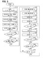
- a target charge amount setting signal So representing the target charge amount Q calculated in S130 is output to the non-inverting input terminal (+) of the determining circuit 80 (the comparator CMP1).
- S170 It is checked in S170 whether the driving signal Sd is input or not. If it is determined in S170 that no driving signal Sd is input, the processing of S170 is repetitively executed. Conversely, if it is determined that the driving signal Sd is input, the processing proceeds to S180.
- a switching period St representing the timing at which the charging switch SW1 should be turned on is output for a predetermined time.
- a charging switching signal Ss for turning on the charging switch SW1 is output to the gate of the charging switch SW1. Then, it is checked in S220 whether the signal level of the determination signal Sh is low or not.
- S260 it is checked whether the switching period Ts has elapsed from the start of the measurement of the switching period Ts in S190. If it is determined in S260 that the switching period Ts has not yet elapsed, the processing of S260 is repetitively executed. Conversely, if it is determined that the switching period Ts has elapsed, the processing proceeds to S270.
- S270 it is checked whether the charging period Tc has elapsed (been finished) from the start of the measurement of the charging period Tc in S180. If it is determined in S270 that the charging period Tc has not yet been finished, the processing proceeds to S190. Conversely, if it is determined that the charging period Tc has been finished, the output of the cylinder selecting switching signal is stopped, and the processing proceeds to S110.
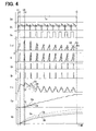
- the driving device 1 when the driving signal Sd is input to the switch controller 50 at time t1 (S170: YES), the switching period signal St and the charging switching signal Ss are output (S200, S210), and also the cylinder selecting switching signal is output to the cylinder selecting switch SWa.
- the charging switch SW1 is turned on to make the charging circuit 30 conductive, so that buffer capacitor current Ic1 flows from the buffer capacitor C1 through the charging circuit 30 to the piezoelectric actuator P1.
- the buffer capacitor current Ic1 gradually increases on the basis of the time constant determined by the inductor L1 and the capacitance of the piezoelectric actuator P1, and thus the charge amount represented by the integration signal Si also increases.
- the output level of the determination signal Sh is switched to low level (S220: YES), and the output of the charging switching signal Ss is stopped (S230).
- the charging switch SW1 is turned off to block the charging circuit 30, and a flywheel current flows to the piezoelectric actuator P1 through the parasitic diode D2 by the energy accumulated through the inductor L1.
- the flywheel current is gradually reduced through the discharge of the energy accumulated in the inductor L1.
- the charging switch controller 90 outputs the integration reset signal Sr for a predetermined time, so that the integration reset switch SW4 is turned on and the charges accumulated in the capacitor C2 is discharged (that is, the integration signal Si is reset).
- the operation that the charging switch SW1 is turned on at the period corresponding to each switching period Ts and the charging switch SW1 is turned off every time the integration signal Si reaches the target charge amount Q is repeated until a time t5 at which the charging period Tc has elapsed from the time t1.
- One-dotted chain line of Fig. 4 represents a case where in place of the piezoelectric actuators P1 to P4, piezoelectric actuators having a medium capacitance Cm smaller than the electrostatic capacitance (large capacitance Cl represented by a solid line) of the piezoelectric actuators P1 to P4 are used as driving targets in the driving device 1.
- Two-dotted chain line of Fig. 4 represents a case where piezoelectric actuators having further smaller electrostatic capacitance Cs than the electrostatic capacitance of the piezoelectric actuators used in the case indicated by the one-dotted chain line of Fig. 4 are used as driving targets in the driving device 1.
- Fig. 4 the case where the piezoelectric actuators P1 to P4 having large-level electrostatic capacitance Cl are used in the driving device 1 is represented by the solid line, the case where the piezoelectric actuators P1 to P4 having medium electrostatic capacitance Cm are used in the driving device is represented by one-dotted chain line, and the case where the piezoelectric actuators P1 to P4 having small-level electrostatic capacitance Cs are used in the driving device is represented by two-dotted chain line.
- the output start timing of the charging period signal St is not varied. Therefore, with respect to the signals Ss, Sh, Sr when the electrostatic capacitance is in the medium level or small level, the output stop timing of the charging switching signal Ss and the variation patterns of the signals Sh, Sr are delayed as compared with those when the electrostatic capacitance is in the large level, as in the case of the buffer capacitance current Ic1 and the variation pattern of the integration signal Si.
- the charging switch SW1 is turned on at a fixed period, and also the charging switch SW1 is turned off every time the charge amount represented by the integration signal Si reaches the target charge amount Q.
- the switching period Ts when the charging switch SW1 is turned on during the charging period Tc is fixed, and the charge energy in one turn-on operation of the charging switch SW1 can be also fixed irrespective of temperature variation. Therefore, the expansion rate of the piezoelectric actuators P1 to P4 (that is, the expanding behavior of the piezoelectric actuators P1 to P4 through one charging operation) during the charging period Tc can be set to a desired expansion rate.
- the timing of the fuel injection of the injector can be prevented from being varied due to the variation of the electrostatic capacitance.
- the integration value of the buffer capacitor current Ic1 flowing from the buffer capacitor C1 to the piezoelectric actuators P1 to P4 is calculated, the charge energy Ep to be charged in the piezoelectric actuators P1 to P4 per unit time can be derived. Therefore, in the driving device 1 of the first embodiment, when the integration signal Si reaches the target charge amount Q, the charging switch SW1 is turned off.
- the charge energy Ep can be estimated by merely deriving the integration value of the buffer capacitor current Ic1, and thus the construction of the driving device 1 can be simplified.
- the target value Q is determined on the basis of the voltage value of the buffer capacitor C1 and the energy instruction value E, and thus the expansion rate of the piezoelectric actuators P1 to P4 can be set to be identical even when the voltage value V of the buffer capacitor C1 varies.
- the power supply circuit 12 operates as a DC power source
- the parasitic diode D1 operates as a first diode
- the parasitic diode D2 operates as a second diode.
- the input of the driving signal Sd is a driving instruction
- the stop of the driving signal Sd is a driving stop instruction.
- the switch controller 50 operates as a charge/discharge control section
- the current detecting resistor R1 operates as a current detecting section
- the current integration circuit 70 operates as an estimating section
- the processing of S170 to S270 operates as a charge switch driving section.
- the processing of S120 and S130 operates as a target value setting section.
- the driving device 1 of the second embodiment is different from the first embodiment in the connecting position of the current detecting resistor R1 and the stop timing of the output of the integration reset signal Sr.
- the current detecting resistor R1 is connected between the end portion of the parallel circuit 10 at the cylinder selecting switch (SWa to SWd) side and the ground line.
- the current integration circuit 70 integrates not only the buffer capacitor current, but also the flywheel current.
- the output stop timing of the integration reset signal Sr is set to the time when the switching period signal St is next output, at time t3 for example, as shown in Fig. 6.
- the output of the integration reset signal Sr is stopped when the charging switch controller 90 finishes the processing of S200.
- the charge energy in one turn-on operation of the charging switch SW1 can be fixed while the switching period Ts when the charging switch SW1 is turned on is fixed, and thus the same advantage as the first embodiment can be acquired.
- the driving device of the third embodiment is different from the driving device 1 of the first embodiment so that the target charge amount Q is not fixed among the switching periods Ts in the charging period Ts.
- the target charge amount Q1 in the first ON-period of the charging switch SW1 is smaller than the target charge amount Q of the second and subsequent ON-periods.
- the target charge amount Q1 is stored in ROM of the charging switch controller 90, and the charging switch controller 90 calculates the target charge amount Q of the second and subsequent ON-periods of the charging switch SW1 on the basis of the target charge amount Q1 and the total charge amount Qt.
- the charging switch controller 90 controls the turn-off of the charging switch SW1 by using the target charge amount Q1 in the first ON-period of the charging switch SW1, and also controls the turn-off of the charging switch SW1 by using the target charge amount Q larger than the target charge amount Q1 in the second and subsequent ON-periods of the charging switch SW1.
- the energy instruction value E, the charging period Tc, the switching period Ts and the switching frequency N are first read from ROM in S310, and also the voltage value V of the buffer capacitor C1 is acquired from the boosting control circuit 18.
- the target charge amount Q1 in the first ON-period of the charging switch SW1 is read from ROM.
- the value (Qt-Q1) acquired by subtracting the target charge amount Q1 from the total charge amount Qt is divided by the value (N-1) acquired by subtracting 1 from the switching frequency N, thereby calculating the target charge value Q in each of the second and subsequent ON-periods of the charging switch SW1.
- Q Qt - Q ⁇ 1 / N - 1
- the integration reset signal Sr is output for a predetermined time.
- a target charge amount signal So representing the target charge amount Q1 in the first ON-period of the charging switching SW1 is output.
- S370 it is checked in S370 whether the signal level of the determination signal Sh is high or not. If it is determined in S370 that the signal level of the determination signal Sh is not high, the processing of S370 is repetitively executed. Conversely, if it is determined in S370 that the signal level of the determination signal Sh is high, the processing proceeds to S380.
- S380 it is checked whether the driving signal Sd is input or not. Then, if it is determined in S380 that no driving signal Sd is input, the processing of S380 is repetitively executed. Conversely, if it is determined that the driving signal Sd is input, the processing proceeds to S390.
- S390 the measurement of the charging period Ts is started, and the cylinder selecting switching signal is output.
- the subsequent S400 the measurement of the switching period Ts is started.
- the switching period signal St is output for a predetermined time, and in the subsequent S420, the charging switching signal Ss is output.
- S430 it is checked whether the signal level of the determination signal Sh is low or not. Then, if it is determined in S430 that the signal level of the determination signal Sh is not low, the processing of S430 is repetitively executed. Conversely, if it is determined in S430 that the signal level of the determination signal Sh is low, the processing proceeds to S440.
- S470 it is checked whether the signal level of the determination signal Sh is high or not. If it is determined in S470 that the signal level of the determination signal Sh is not high, the processing of S470 is repetitively executed. Conversely, if it is determined in S470 that the signal level of the determination signal Sh is high, the processing proceeds to S480.
- S480 it is checked whether the switching period Ts has elapsed or not from the time when the measurement of the switching period Ts is started in S400. If it is determined in S480 that the switching period Ts has not yet elapsed, the processing of S480 is repetitively executed. Conversely, if it is determined in S480 that the switching period has elapsed, the processing proceeds to S490.
- S490 it is checked whether the charging period Tc has elapsed (finished) or not from the time when the measurement of the charging period Tc is started in S390. If it is determined in S490 that the charging period Tc has not yet elapsed, the processing returns to S400. Conversely, if it is determined in S490 that the charging period Tc has elapsed (finished), the output of the cylinder selecting switching signal is stopped, and the processing proceeds to S310.
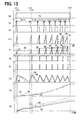
- the target charge amount Q1 is input to the non-inverting input terminal (+) of the determining circuit 80 (S360), and when the driving signal Sd is input to the switch controller 50 at time t6 as shown in Fig. 8 (S380: YES), the switching period signal St and the charging switching signal Ss are output (S410, S420), and the cylinder selecting switching signal is output to the cylinder selecting switch SWa.
- the buffer capacitor current flows from the buffer capacitor C1 through the charging circuit 30 to the piezoelectric actuator P1. Then, when at time t7 the charge amount represented by the integration signal Si reaches the target charge amount Q1, the output level of the determination signal Sh is switched to low (S430: YES), the output of the charging switch signal Ss is stopped (S440).
- the charging switching controller 90 outputs the integration reset signal Sr for a predetermined time, and the target charge amount Q larger than the target charge amount Q1 is input to the non-inverting input terminal (+) of the determining circuit 80 (S460).
- the switching period Ts when the charging switch SW1 is turned on in the charging period Tc is fixed, and the charge energy in the first turn-on operation of the charging switch SW1 can be fixed irrespective of temperature variation, so that the same advantage as the first embodiment can be acquired.
- the target charge amount every switching period Ts in the charging period Tc is set so that the target charge amount Q1 in the first ON-period of the charging switch SW1 is smaller than the target charge amount Q of each of the second and subsequent ON-periods. Therefore, the charging energy to be accumulated into the piezoelectric actuators P1 to P4 at the charging start time (first ON-period of the charging switch SW1) can be reduced to be less than the charging energy when the target charge amount Q of each switching period Ts is set to be identical among the respective switching periods Ts (one-dotted chain line of Fig. 8).
- the load imposed on the piezoelectric actuators P1 to P4 at the charging start time can be reduced, and thus the lifetime and reliability of the piezoelectric actuators can be enhanced. In addition, occurrence of operating sounds can be suppressed.
- the switching period Ts is set so as to become shorter every time the charging switch SW1 is turned on.
- the switching period Ts may be set to be fixed as in the case of the first and second embodiments.
- the target charge amount Q1 in the first ON-period of the charging switch SW1 may be set to any value insofar as it is smaller than the target charge amount Q in the second and subsequent ON-periods.
- the target charge amount Q1 in the first ON-period of the charging switch SW1 is stored in ROM.
- the target charge amount Q1 may be set and changed by the user or the like.
- the driving device of the fourth embodiment is different from the driving device 1 of the first embodiment in that the switching period Ts is not fixed, but it is set to be shorter every time the charging switch SW1 is once turned on.
- the switching period Ts(n) of the fourth embodiment is set on the basis of a value which is acquired by an experiment or the like in advance so that no flywheel has been already prevented from flowing in the discharge circuit 40 at the output time of the switching period signal St (the turn-on time of the charging switch SW1) even when the electrostatic capacitance of the piezoelectric actuators P1 to P4 varies).
- the period at which the flywheel current flows in the discharge circuit 40 during charging operation is measured by the experiment or the like in advance, and the switching period Ts(n) is set on the basis of the measurement result.
- the charging switch controller 90 of the driving device starts the processing of Fig. 9, in S510, the energy instruction value E, the charging period Tc, the switching period Ts(n) and the switching frequency N are read from ROM, and also the voltage V of the buffer capacitor C1 is acquired from the boosting control circuit 18.
- the energy instruction value E is divided by the voltage value V to calculate the total charge amount Qt (Qt+E/V).
- n is set to 1.
- the integration reset signal Sr is output for a predetermined time.
- the target charge amount setting signal So representing the target charge amount Q is output.
- S570 it is checked whether the signal level of the determination signal Sh is high or not. If it is determined in S570 that the signal level of the determination signal Sh is not high, the processing of S570 is repetitively executed. Conversely, if it is determined in S570 that the signal level of the determination signal Sh is high, the processing proceeds to S580.
- S580 it is checked whether the driving signal Sd is input. If it is determined in S580 that no driving signal Sd is input, the processing of S580 is repetitively executed. Conversely, if it is determined in S580 that the driving signal Sd is input, the processing proceeds to S590.
- S670 it is checked whether the switching period Ts(n) has elapsed from the start time of the measurement of the switching period Ts(n) in S600. If it is determined in S670 that the switching period Ts(n) has not yet elapsed, the processing of S670 is repetitively executed. Conversely, if it is determined that the switching period Ts(n) has elapsed, the processing proceeds to S680.
- n is incremented by adding 1 to n. Then, it is determined in S690 whether the charging period Tc has elapsed (finished) from the time when the measurement of the charging period Tc is started in S590.
- the driving device of the fourth embodiment irrespective of the temperature variation, the charge energy in one turn-on operation of the charging switch SW1 can be also fixed while the switching period Ts at the ON-time of the charging switch SW1 in the charging period Tc is fixed. Therefore, the same advantage as the first embodiment can be acquired. Accordingly, as compared with the first embodiment, the expansion rate of the piezoelectric actuators P1 to P4 can be more efficiently suppressed from being varied due to variation of the electrostatic capacitance.
- the charging switch SW1 is turned on during charging operation before flow of the flywheel current is stopped. Therefore, all the energy accumulated in the inductor L1 is not necessarily discharged, and thus a residual amount of energy is carried over to the next operation. Therefore, when the electrostatic capacitance of the piezoelectric actuators P1 to P4 varies, the energy to be carried over is also varied. Accordingly, the charge amount every OFF-period of the charging switch SW1 is varied, and the expansion rate every electrostatic capacitance is slightly dispersed.
- the switching period Ts(n) is set so that no flywheel current has been already prevented from flowing to the discharge circuit 40 at the output time of the switching period signal St even when the electrostatic capacitance varies.
- the variation of the expansion rate of the piezoelectric actuators P1 to P4 due to the variation of the electrostatic capacitance can be more efficiently suppressed as compared with the first embodiment.
- the switching period Ts(n) is set so that flywheel current has been already prevented from flowing to the discharge circuit 40 at the time when the switching period signal St is output, current (through current) is prevented from flowing in the opposite direction flows to the parasitic diode D2 of the discharge switch SW2 at the time when the charging switch SW1 is turned on. Accordingly, occurrence of noise and loss can be suppressed.
- the driving device according to the fifth embodiment when the electrostatic capacitance of the piezoelectric actuators P1 to P4 is small, a period at which the flow of flywheel current to the discharging circuit 40 is stopped in the charging operation is measured by an experiment or the like.
- the switching period Ts(n) is set on the basis of the measurement result.
- the switching period Ts(n) is set on the basis of the case where the electrostatic capacitance of the piezoelectric actuators P1 to P4 is large.
- the switching period Ts(n) is set on the basis of the case where the electrostatic capacitance of the piezoelectric actuators P1 to P4 is small.
- the charge energy in one turn-on operation of the charging switch SW1 can be also fixed while the switching period Ts at the ON-time of the charging switch SW1 in the charging period Tc is fixed. Therefore, the same advantage as the first embodiment can be acquired.
- the switching period Ts is set on the basis of the case where the electrostatic capacitance of the piezoelectric actuators P1 to P4 is small, and thus the switching period Ts can be set to a smaller value as compared with the fourth embodiment.
- the switching frequency N can be set to a larger value, and thus the piezoelectric actuators P1 to P4 can be charged so as to expand more smoothly.
- the driving device of the sixth embodiment is different from the driving device 1 of the first embodiment in that the target charge amount Q is not fixed and the target charge amount Qn is set so that the variation amount G of the voltage per unit time applied to the piezoelectric actuators P1 to P4 is equal among the respective switching periods Ts(n).
- the target charge amount Qn is calculated by using the following equation (2) so that the variation amount G of the voltage is equal among the respective switching periods Ts(n).
- the target charge amount Qn can be calculated as above for the following reasons.
- the total charge amount Qt to be discharged from the buffer capacitor C1 within the charging period Tc corresponds to the value acquired by dividing the energy instruction value E by the voltage value V as defined in the following equation (3).
- Q t E / V
- the variation amount G of the voltage corresponds to the value acquired by dividing the voltage value Va by the charging period Tc as defined in the following equation (4).
- Va represents the voltage value applied to the piezoelectric actuators P1 to P4 when the charging is finished.
- G V a / T c
- the variation amount G1 of the voltage when the charging switch SW1 is first turned off corresponds to the value acquired by dividing the voltage value V1 by the switching period Ts(1) (that is, the period Ts(1) when the charging switch SW1 is first turned on) as indicated by the following equation (5).
- G 1 V 1 / T s 1
- V a 2 ⁇ E C
- V a 2 ⁇ Q t ⁇ V C
- V 1 2 ⁇ Q 1 ⁇ V C
- the variation amount G1 of the voltage can be represented by the following equation (10) by substituting the right-hand side of the equation (9) into V1 of the equation (5).
- G 1 2 ⁇ Q 1 ⁇ V / C T s 1
- Q 1 Q t ( T s 1 T c ⁇ ) 2
- the target charge amount Q2 when the charging switch SW1 is secondly turned on can be likewise derived.
- V 2 2 ⁇ Q 1 + Q 2 ⁇ V C
- G 2 2 ⁇ Q 1 + Q 2 ⁇ V / C T s 1 + T s 2
- the variation amount G2 of the voltage may be set to be equal to the variation amount G of the voltage, and thus the target charge amount Q2 can be represented by the following equation (14) on the basis of the equations (8) and (13).
- Q 2 Q t ( T 1 + T 2 T c ⁇ ) 2 - Q 1
- the target charge amount Q3 when the charging switch SW1 is thirdly turned on can be represented by the following equation (15).
- Q 3 Q t ( T 1 + T 2 + T 3 T c ⁇ ) 2 - Q 1 + Q 2
- the target charge amount Qn when the charging switch SW1 is turned on at the n-th time can be represented by the equation (2) from the equations (11), (14) and (15).
- the charging switch controller 90 of the driving device starts the processing of Fig. 12, in S710 the energy instruction value E, the charging period Tc, the switching period Ts(n) and the switching frequency N are read out from ROM, and also the voltage value V of the buffer capacitor C1 is acquired from the boosting control circuit 18.
- Qt E/V
- the target charge amount Qn that is, the first target charge amount Q1
- the integration reset signal Sr is output for a predetermined time in S750, and the target charge amount setting signal So representing the target charge amount Q1 is output in the subsequent S760. Then, it is checked in S770 whether the signal level of the determination signal Sh is high or not.
- S780 it is checked whether the driving signal Sd is input. If it is determined in S780 that no driving signal Sd is input, the processing of S780 is repetitively executed. Conversely, if it is determined in S780 that the driving signal Sd is input, the processing proceeds to S790.
- the measurement of the charging period Tc is started, and also the cylinder selecting switching signal is output.
- the measurement of the switching period Ts(n) is started, and the switching period signal St is output for a predetermined time in the subsequent S810.
- the charging switching signal Ss is output. It is checked in the subsequent S830 whether the signal level of the determination signal Sh is low or not.
- n is incremented by added 1 to the last value.
- the target charge amount Qn is calculated on the basis of the equation (2).
- the target charge amount setting signal So representing the target charge amount Qn calculated in S880 is output. It is checked in the subsequent S900 whether the signal level of the determination signal Sh is high.
- S910 it is checked whether the switching period Ts(n-1) has elapsed from the start of the measurement in S800. If it is determined in S910 that the switching period Ts(n-1) has not elapsed, the processing of S910 is repetitively executed. Conversely, it is checked in S910 that the switching period Ts(n-1) has elapsed, the processing proceeds to S920.
- S920 it is checked whether the charging period Tc has elapsed (finished) from the start of the measurement in S790. If it is determined in S920 that the charging period Tc has not finished, the processing proceeds to S800. Conversely, if it is determined in S920 that the charging period Tc has finished, the output of the cylinder selecting switching signal is stopped, and the processing proceeds to S710.
- the target charge amount Q1 is input to the non-inverting input terminal(+) of the determining circuit 80 (S760).
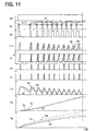
- the driving signal Sd is input to the switch controller 50 at time t11 as shown in Fig. 13 (S780: YES)
- both the switching period signal St and the charging switching signal Ss are output (S810, S820), and the cylinder selecting switching signal is output to the cylinder selecting switch SWa.
- the buffer capacitor current Ic1 flows from the buffer capacitor C1 through the charging circuit 30 to the piezoelectric actuator P1 as described above.
- the flywheel current flows through the parasitic diode D2 to the piezoelectric actuator P1 as described above.
- the charging switch controller 90 outputs the integration reset signal Sr for a predetermined time, and the target charge amount Q2 is calculated and input to the non-inverting input terminal (+) of the determining circuit 80 (S880, S890).
- the charge energy in one turn-on operation of the charging switch SW1 can be fixed while the switching period Ts when the charging switch SW1 is turned on is fixed.
- the same advantage as the first embodiment can be acquired.
- the variation amount Gn of the voltage every ON-period of the charging switch SW1 is set to be equal, so that the expansion rate of the piezoelectric actuators P1 to P4 every ON-period of the charging switch SW1 can be set to be equal.
- the switching period Ts(n) is set so that the flywheel current has been already prevented from flowing through the discharge circuit 40 at the output time of the switching period St.
- the switching period Ts(n) as described above can be set.
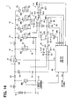
- the driving device 1 is designed so that the current detecting resistor R10 for detecting the charge current flowing through the piezoelectric actuators P1 to P4 under charging operation, a current detecting circuit 100 for detecting the charge current and a determining circuit 110 for determining whether the flow of the charge current detected by the current detecting circuit 100 is stopped are additionally provided to the driving device 1 of the first embodiment (Fig. 2).
- the current detecting resistor R10 is connected between an end portion at the cylinder selecting switch (SWa to SWd) side of the parallel circuit 10 and the ground line.
- the current detecting circuit 100 has resistors R11, R12, R13, R14 and an operational amplifier OP3.
- the connection point between the current detecting resistor R10 and the parallel circuit 10 is connected through the resistor R11 to the non-inverting input terminal (+) of the operational amplifier OP3.
- the connection point between the current detecting resistor R10 and the ground line is connected through the R12 to the inverting input terminal (-) of the operational amplifier OP3.
- a current detecting signal Sc2 represented by the voltage value acquired by amplifying the potential between both terminals of the current detecting resistor R10 at a predetermined gain is output from the output terminal of the operational amplifier OP3.
- the reference voltage Vref is input through the resistor R14 to the non-inverting input terminal (+) of the operational amplifier OP3.
- the determination circuit 110 has resistors R15, R16, R17 and a comparator CMP2.
- the current detection signal Sc2 is input through the resistor R15 to the inverting input terminal (-) of the comparator CMP2, and a current zero threshold value signal Sz output from the charging switch controller 90 is input through the resistor R16 to the non-inverting input terminal (+) of the comparator CMP2.
- the current zero threshold value signal Sz is used as a threshold value with which the determining circuit 110 checks whether no charge current (more specifically, the flywheel current) has just flowed to the piezoelectric actuators P1 to P4, Thus, it is input to the non-inverting input terminal (+).
- the determining circuit 110 is constructed as a comparator CMP2 having hysteresis (Schmidt trigger) for switching the magnitude of the threshold value represented by the current zero threshold value signal in two stages in accordance with the output signal of the comparator CMP2.
- the driving device of this embodiment when the signal level of the output signal from the determining circuit 110 is switched from low level to high level during charging operation, the flow of the charge current (more specifically, flywheel current) to the piezoelectric actuators P1 to P4 has been just stopped.
- the charge current more specifically, flywheel current
- the time when the flow of the flywheel current has been just stopped can be known, and thus the switching period Ts(n) can be set so that the flow of the flywheel current to the discharge circuit 40 has been already stopped at the output time of the switching period signal St.
- the setting of the switching period Ts(n) may be carried out at the shipping time of a vehicle in which the driving device is mounted, or carried out periodically.
- the above embodiments may be modified in various ways.
- the switch controller 90 may turn on/off the boosting switch SW3.
Landscapes
- Engineering & Computer Science (AREA)
- Chemical & Material Sciences (AREA)
- Combustion & Propulsion (AREA)
- Mechanical Engineering (AREA)
- General Engineering & Computer Science (AREA)
- General Electrical Machinery Utilizing Piezoelectricity, Electrostriction Or Magnetostriction (AREA)
Applications Claiming Priority (1)
| Application Number | Priority Date | Filing Date | Title |
|---|---|---|---|
| JP2006173883A JP2008005649A (ja) | 2006-06-23 | 2006-06-23 | ピエゾアクチュエータの駆動装置 |
Publications (3)
| Publication Number | Publication Date |
|---|---|
| EP1870947A2 true EP1870947A2 (fr) | 2007-12-26 |
| EP1870947A3 EP1870947A3 (fr) | 2008-11-19 |
| EP1870947B1 EP1870947B1 (fr) | 2010-11-24 |
Family
ID=38603417
Family Applications (1)
| Application Number | Title | Priority Date | Filing Date |
|---|---|---|---|
| EP07011623A Not-in-force EP1870947B1 (fr) | 2006-06-23 | 2007-06-13 | Dispositif de commande pour actionneur piézoélectrique |
Country Status (4)
| Country | Link |
|---|---|
| US (1) | US7474035B2 (fr) |
| EP (1) | EP1870947B1 (fr) |
| JP (1) | JP2008005649A (fr) |
| DE (1) | DE602007010692D1 (fr) |
Cited By (1)
| Publication number | Priority date | Publication date | Assignee | Title |
|---|---|---|---|---|
| EP2144308A3 (fr) * | 2008-07-07 | 2011-12-21 | Nippon Soken, Inc. | Dispositif de commande d'actionneur piézoélectrique |
Families Citing this family (12)
| Publication number | Priority date | Publication date | Assignee | Title |
|---|---|---|---|---|
| US7781943B1 (en) * | 2007-01-24 | 2010-08-24 | Micro Strain, Inc. | Capacitive discharge energy harvesting converter |
| DE102007008201B3 (de) * | 2007-02-19 | 2008-08-14 | Siemens Ag | Verfahren zur Regelung einer Einspritzmenge eines Injektors einer Brennkraftmaschine |
| JP4434248B2 (ja) * | 2007-08-22 | 2010-03-17 | 株式会社デンソー | ピエゾアクチュエータ駆動装置 |
| JP4925976B2 (ja) * | 2007-08-29 | 2012-05-09 | 株式会社ケーヒン | 内燃機関制御装置 |
| US8277203B2 (en) * | 2009-07-02 | 2012-10-02 | Sunonwealth Electric Machine Industry Co., Ltd. | DC fan of inner rotor type |
| JP5260597B2 (ja) * | 2010-05-27 | 2013-08-14 | 日立オートモティブシステムズ株式会社 | 内燃機関の燃料噴射装置及び制御方法 |
| US9270206B2 (en) | 2012-01-23 | 2016-02-23 | Alfred E. Mann Foundation For Scientific Research | Methods and systems for applying charge to a piezoelectric element |
| JP6413582B2 (ja) * | 2014-10-03 | 2018-10-31 | 株式会社デンソー | 内燃機関の制御装置 |
| US10853549B2 (en) * | 2016-07-26 | 2020-12-01 | Omnitek Partners Llc | Method and apparatus for simulating the generated charge profile of piezoelectric elements due to arbitrary shock loading |
| US11081635B1 (en) | 2017-04-10 | 2021-08-03 | Maxim Integrated Products, Inc. | Method and apparatus for driving a piezoelectric transducer with stored charge recovery |
| CN108414959B (zh) * | 2018-04-04 | 2024-02-23 | 京东方科技集团股份有限公司 | 压电传感器检测电路、阵列压电传感器电路及控制方法 |
| JP7067233B2 (ja) * | 2018-04-20 | 2022-05-16 | 株式会社デンソー | 噴射制御装置 |
Family Cites Families (19)
| Publication number | Priority date | Publication date | Assignee | Title |
|---|---|---|---|---|
| US4732129A (en) * | 1985-04-15 | 1988-03-22 | Nippon Soken, Inc. | Control apparatus for electroexpansive actuator enabling variation of stroke |
| JP2870336B2 (ja) | 1992-12-04 | 1999-03-17 | トヨタ自動車株式会社 | 圧電素子駆動回路 |
| DE19632837A1 (de) * | 1996-08-14 | 1998-02-19 | Siemens Ag | Vorrichtung und Verfahren zum Ansteuern wenigstens eines kapazitiven Stellgliedes |
| DE19644521A1 (de) * | 1996-10-25 | 1998-04-30 | Siemens Ag | Verfahren und Vorrichtung zum Ansteuern eines kapazitiven Stellgliedes |
| DE19652801C1 (de) * | 1996-12-18 | 1998-04-23 | Siemens Ag | Verfahren und Vorrichtung zum Ansteuern wenigstens eines kapazitiven Stellgliedes |
| DE19723932C1 (de) * | 1997-06-06 | 1998-12-24 | Siemens Ag | Verfahren zum Ansteuern wenigstens eines kapazitiven Stellgliedes |
| DE19723935C1 (de) * | 1997-06-06 | 1998-12-17 | Siemens Ag | Vorrichtung und Verfahren zum Ansteuern wenigstens eines kapazitiven Stellgliedes |
| ATE446590T1 (de) * | 2000-04-01 | 2009-11-15 | Bosch Gmbh Robert | Verfahren und vorrichtung zur regelung von spannungen und spannungsgradienten zum antrieb eines piezoelektrischen elements |
| DE10017367B4 (de) * | 2000-04-07 | 2006-12-28 | Siemens Ag | Verfahren und Vorrichtung zum Ansteuern wenigstens eines kapazitiven Stellgliedes |
| US6661285B1 (en) * | 2000-10-02 | 2003-12-09 | Holosonic Research Labs | Power efficient capacitive load driving device |
| JP4479113B2 (ja) * | 2001-02-23 | 2010-06-09 | 株式会社デンソー | ピエゾアクチュエータ駆動回路および燃料噴射装置 |
| US7190102B2 (en) * | 2002-09-05 | 2007-03-13 | Viking Technologies, L.C. | Apparatus and method for charging and discharging a capacitor to a predetermined setpoint |
| US6979933B2 (en) * | 2002-09-05 | 2005-12-27 | Viking Technologies, L.C. | Apparatus and method for charging and discharging a capacitor |
| JP3913687B2 (ja) * | 2003-02-17 | 2007-05-09 | 株式会社デンソー | ピエゾアクチュエータ駆動回路および燃料噴射装置 |
| JP4353781B2 (ja) * | 2003-02-27 | 2009-10-28 | 株式会社日本自動車部品総合研究所 | ピエゾアクチュエータ駆動回路 |
| JP4104498B2 (ja) * | 2003-06-26 | 2008-06-18 | 株式会社日本自動車部品総合研究所 | ピエゾアクチュエータ駆動回路 |
| JP4615967B2 (ja) * | 2004-11-17 | 2011-01-19 | 株式会社日本自動車部品総合研究所 | ピエゾインジェクタの駆動装置 |
| JP4624134B2 (ja) | 2005-02-25 | 2011-02-02 | 株式会社デンソー | ピエゾアクチュエータの駆動回路 |
| JP4853201B2 (ja) * | 2006-09-27 | 2012-01-11 | 株式会社デンソー | インジェクタ駆動装置及びインジェクタ駆動システム |
-
2006
- 2006-06-23 JP JP2006173883A patent/JP2008005649A/ja active Pending
-
2007
- 2007-06-07 US US11/808,180 patent/US7474035B2/en not_active Expired - Fee Related
- 2007-06-13 DE DE602007010692T patent/DE602007010692D1/de active Active
- 2007-06-13 EP EP07011623A patent/EP1870947B1/fr not_active Not-in-force
Cited By (1)
| Publication number | Priority date | Publication date | Assignee | Title |
|---|---|---|---|---|
| EP2144308A3 (fr) * | 2008-07-07 | 2011-12-21 | Nippon Soken, Inc. | Dispositif de commande d'actionneur piézoélectrique |
Also Published As
| Publication number | Publication date |
|---|---|
| EP1870947B1 (fr) | 2010-11-24 |
| DE602007010692D1 (de) | 2011-01-05 |
| JP2008005649A (ja) | 2008-01-10 |
| US7474035B2 (en) | 2009-01-06 |
| EP1870947A3 (fr) | 2008-11-19 |
| US20070296307A1 (en) | 2007-12-27 |
Similar Documents
| Publication | Publication Date | Title |
|---|---|---|
| EP1870947B1 (fr) | Dispositif de commande pour actionneur piézoélectrique | |
| US7404396B2 (en) | Multiple discharge ignition control apparatus and method for internal combustion engines | |
| JP5151783B2 (ja) | 昇圧電源装置 | |
| US8878544B2 (en) | Electric leakage sensing apparatus | |
| US10253744B2 (en) | Flyback switching mode power supply with voltage control and a method thereof | |
| US5982604A (en) | Power supply apparatus for electronic control unit in automotive vehicle | |
| KR101411000B1 (ko) | 컨버터 및 그 구동방법 | |
| EP0611881A1 (fr) | Dispositif pour régler l'injection de carburant pour moteur à combustion interne | |
| US7732976B2 (en) | Piezoelectric actuator drive device | |
| JP6151956B2 (ja) | 絶縁型スイッチング電源装置 | |
| JP4306769B2 (ja) | ピエゾアクチュエータ駆動装置 | |
| JP2019060306A (ja) | インジェクタ駆動装置 | |
| JP2870324B2 (ja) | 圧電素子の駆動回路 | |
| JP2005330934A (ja) | インジェクタ駆動装置 | |
| KR101206887B1 (ko) | 용량성 부하를 제어하기 위한 방법 및 장치 | |
| JP4630165B2 (ja) | Dc−dcコンバータ | |
| JP4624134B2 (ja) | ピエゾアクチュエータの駆動回路 | |
| JP2005016431A (ja) | ピエゾアクチュエータ駆動回路 | |
| JP2016054628A (ja) | 電源装置および電源装置の充電方法 | |
| JP2012147534A (ja) | 昇圧装置および昇圧回路 | |
| JP2002237410A (ja) | 電磁弁駆動回路 | |
| JPH09135568A (ja) | Dc/dcコンバータ | |
| JP2003328914A (ja) | Dc/dcコンバータ式内燃機関用点火装置 | |
| CN113196638A (zh) | Dcdc转换器 | |
| JP2786870B2 (ja) | Dc/dcコンバータ |
Legal Events
| Date | Code | Title | Description |
|---|---|---|---|
| PUAI | Public reference made under article 153(3) epc to a published international application that has entered the european phase |
Free format text: ORIGINAL CODE: 0009012 |
|
| AK | Designated contracting states |
Kind code of ref document: A2 Designated state(s): AT BE BG CH CY CZ DE DK EE ES FI FR GB GR HU IE IS IT LI LT LU LV MC MT NL PL PT RO SE SI SK TR |
|
| AX | Request for extension of the european patent |
Extension state: AL BA HR MK YU |
|
| PUAL | Search report despatched |
Free format text: ORIGINAL CODE: 0009013 |
|
| AK | Designated contracting states |
Kind code of ref document: A3 Designated state(s): AT BE BG CH CY CZ DE DK EE ES FI FR GB GR HU IE IS IT LI LT LU LV MC MT NL PL PT RO SE SI SK TR |
|
| AX | Request for extension of the european patent |
Extension state: AL BA HR MK RS |
|
| 17P | Request for examination filed |
Effective date: 20090518 |
|
| AKX | Designation fees paid |
Designated state(s): DE FR IT |
|
| GRAP | Despatch of communication of intention to grant a patent |
Free format text: ORIGINAL CODE: EPIDOSNIGR1 |
|
| GRAS | Grant fee paid |
Free format text: ORIGINAL CODE: EPIDOSNIGR3 |
|
| GRAA | (expected) grant |
Free format text: ORIGINAL CODE: 0009210 |
|
| AK | Designated contracting states |
Kind code of ref document: B1 Designated state(s): DE FR IT |
|
| REF | Corresponds to: |
Ref document number: 602007010692 Country of ref document: DE Date of ref document: 20110105 Kind code of ref document: P |
|
| PLBE | No opposition filed within time limit |
Free format text: ORIGINAL CODE: 0009261 |
|
| STAA | Information on the status of an ep patent application or granted ep patent |
Free format text: STATUS: NO OPPOSITION FILED WITHIN TIME LIMIT |
|
| 26N | No opposition filed |
Effective date: 20110825 |
|
| REG | Reference to a national code |
Ref country code: DE Ref legal event code: R097 Ref document number: 602007010692 Country of ref document: DE Effective date: 20110825 |
|
| PGFP | Annual fee paid to national office [announced via postgrant information from national office to epo] |
Ref country code: IT Payment date: 20130619 Year of fee payment: 7 Ref country code: FR Payment date: 20130624 Year of fee payment: 7 |
|
| REG | Reference to a national code |
Ref country code: FR Ref legal event code: ST Effective date: 20150227 |
|
| PG25 | Lapsed in a contracting state [announced via postgrant information from national office to epo] |
Ref country code: IT Free format text: LAPSE BECAUSE OF NON-PAYMENT OF DUE FEES Effective date: 20140613 |
|
| PG25 | Lapsed in a contracting state [announced via postgrant information from national office to epo] |
Ref country code: FR Free format text: LAPSE BECAUSE OF NON-PAYMENT OF DUE FEES Effective date: 20140630 |
|
| PGFP | Annual fee paid to national office [announced via postgrant information from national office to epo] |
Ref country code: DE Payment date: 20150619 Year of fee payment: 9 |
|
| REG | Reference to a national code |
Ref country code: DE Ref legal event code: R119 Ref document number: 602007010692 Country of ref document: DE |
|
| PG25 | Lapsed in a contracting state [announced via postgrant information from national office to epo] |
Ref country code: DE Free format text: LAPSE BECAUSE OF NON-PAYMENT OF DUE FEES Effective date: 20170103 |