EP1871157A2 - Module de protection EMI - Google Patents
Module de protection EMI Download PDFInfo
- Publication number
- EP1871157A2 EP1871157A2 EP07104681A EP07104681A EP1871157A2 EP 1871157 A2 EP1871157 A2 EP 1871157A2 EP 07104681 A EP07104681 A EP 07104681A EP 07104681 A EP07104681 A EP 07104681A EP 1871157 A2 EP1871157 A2 EP 1871157A2
- Authority
- EP
- European Patent Office
- Prior art keywords
- circuit board
- shielding case
- shielding
- connector
- protrusion
- Prior art date
- Legal status (The legal status is an assumption and is not a legal conclusion. Google has not performed a legal analysis and makes no representation as to the accuracy of the status listed.)
- Withdrawn
Links
Images




Classifications
-
- H—ELECTRICITY
- H05—ELECTRIC TECHNIQUES NOT OTHERWISE PROVIDED FOR
- H05K—PRINTED CIRCUITS; CASINGS OR CONSTRUCTIONAL DETAILS OF ELECTRIC APPARATUS; MANUFACTURE OF ASSEMBLAGES OF ELECTRICAL COMPONENTS
- H05K9/00—Screening of apparatus or components against electric or magnetic fields
- H05K9/0007—Casings
- H05K9/002—Casings with localised screening
- H05K9/0022—Casings with localised screening of components mounted on printed circuit boards [PCB]
- H05K9/0024—Shield cases mounted on a PCB, e.g. cans or caps or conformal shields
- H05K9/0026—Shield cases mounted on a PCB, e.g. cans or caps or conformal shields integrally formed from metal sheet
- H05K9/0028—Shield cases mounted on a PCB, e.g. cans or caps or conformal shields integrally formed from metal sheet with retainers or specific soldering features
-
- H—ELECTRICITY
- H01—ELECTRIC ELEMENTS
- H01R—ELECTRICALLY-CONDUCTIVE CONNECTIONS; STRUCTURAL ASSOCIATIONS OF A PLURALITY OF MUTUALLY-INSULATED ELECTRICAL CONNECTING ELEMENTS; COUPLING DEVICES; CURRENT COLLECTORS
- H01R13/00—Details of coupling devices of the kinds covered by groups H01R12/70 or H01R24/00 - H01R33/00
- H01R13/648—Protective earth or shield arrangements on coupling devices, e.g. anti-static shielding
- H01R13/658—High frequency shielding arrangements, e.g. against EMI [Electro-Magnetic Interference] or EMP [Electro-Magnetic Pulse]
- H01R13/6581—Shield structure
- H01R13/6585—Shielding material individually surrounding or interposed between mutually spaced contacts
- H01R13/6586—Shielding material individually surrounding or interposed between mutually spaced contacts for separating multiple connector modules
-
- H—ELECTRICITY
- H01—ELECTRIC ELEMENTS
- H01R—ELECTRICALLY-CONDUCTIVE CONNECTIONS; STRUCTURAL ASSOCIATIONS OF A PLURALITY OF MUTUALLY-INSULATED ELECTRICAL CONNECTING ELEMENTS; COUPLING DEVICES; CURRENT COLLECTORS
- H01R13/00—Details of coupling devices of the kinds covered by groups H01R12/70 or H01R24/00 - H01R33/00
- H01R13/648—Protective earth or shield arrangements on coupling devices, e.g. anti-static shielding
- H01R13/658—High frequency shielding arrangements, e.g. against EMI [Electro-Magnetic Interference] or EMP [Electro-Magnetic Pulse]
- H01R13/6591—Specific features or arrangements of connection of shield to conductive members
- H01R13/6594—Specific features or arrangements of connection of shield to conductive members the shield being mounted on a PCB and connected to conductive members
-
- H—ELECTRICITY
- H05—ELECTRIC TECHNIQUES NOT OTHERWISE PROVIDED FOR
- H05K—PRINTED CIRCUITS; CASINGS OR CONSTRUCTIONAL DETAILS OF ELECTRIC APPARATUS; MANUFACTURE OF ASSEMBLAGES OF ELECTRICAL COMPONENTS
- H05K1/00—Printed circuits
- H05K1/02—Details
- H05K1/0213—Electrical arrangements not otherwise provided for
- H05K1/0216—Reduction of cross-talk, noise or electromagnetic interference
- H05K1/0218—Reduction of cross-talk, noise or electromagnetic interference by printed shielding conductors, ground planes or power plane
-
- H—ELECTRICITY
- H05—ELECTRIC TECHNIQUES NOT OTHERWISE PROVIDED FOR
- H05K—PRINTED CIRCUITS; CASINGS OR CONSTRUCTIONAL DETAILS OF ELECTRIC APPARATUS; MANUFACTURE OF ASSEMBLAGES OF ELECTRICAL COMPONENTS
- H05K9/00—Screening of apparatus or components against electric or magnetic fields
- H05K9/0007—Casings
- H05K9/002—Casings with localised screening
- H05K9/0039—Galvanic coupling of ground layer on printed circuit board [PCB] to conductive casing
-
- H—ELECTRICITY
- H05—ELECTRIC TECHNIQUES NOT OTHERWISE PROVIDED FOR
- H05K—PRINTED CIRCUITS; CASINGS OR CONSTRUCTIONAL DETAILS OF ELECTRIC APPARATUS; MANUFACTURE OF ASSEMBLAGES OF ELECTRICAL COMPONENTS
- H05K2201/00—Indexing scheme relating to printed circuits covered by H05K1/00
- H05K2201/10—Details of components or other objects attached to or integrated in a printed circuit board
- H05K2201/10007—Types of components
- H05K2201/10189—Non-printed connector
-
- H—ELECTRICITY
- H05—ELECTRIC TECHNIQUES NOT OTHERWISE PROVIDED FOR
- H05K—PRINTED CIRCUITS; CASINGS OR CONSTRUCTIONAL DETAILS OF ELECTRIC APPARATUS; MANUFACTURE OF ASSEMBLAGES OF ELECTRICAL COMPONENTS
- H05K2201/00—Indexing scheme relating to printed circuits covered by H05K1/00
- H05K2201/10—Details of components or other objects attached to or integrated in a printed circuit board
- H05K2201/10227—Other objects, e.g. metallic pieces
- H05K2201/10371—Shields or metal cases
-
- H—ELECTRICITY
- H05—ELECTRIC TECHNIQUES NOT OTHERWISE PROVIDED FOR
- H05K—PRINTED CIRCUITS; CASINGS OR CONSTRUCTIONAL DETAILS OF ELECTRIC APPARATUS; MANUFACTURE OF ASSEMBLAGES OF ELECTRICAL COMPONENTS
- H05K2201/00—Indexing scheme relating to printed circuits covered by H05K1/00
- H05K2201/10—Details of components or other objects attached to or integrated in a printed circuit board
- H05K2201/10431—Details of mounted components
- H05K2201/10507—Involving several components
- H05K2201/10515—Stacked components
Definitions
- the present invention relates to a shielding module. More particularly, the present invention relates to a shielding module that is grounded by a circuit board.
- the high frequency and high speed transmission device are introduced with the improvement of the technology.
- In the normal operation of electronic devices there is unintentional generation of electromagnetic energy from the electronic devices.
- the propagation of the electromagnetic energy saturates the external environment and induces unwanted effects.
- the electromagnetic energy level relates to the frequency and the return path thereof. Therefore, the electromagnetic energy from the high speed/frequency electronic device (ex. RF IC) induces unwanted effects on other electronic devices.
- the EMI (Electro Magnetic Interference) protection is important for high speed/frequency applications.
- Fig. 1 is a schematic diagram of a cross sectional view of a common electronic device shielding module.
- the electronic device shielding module includes a circuit board 102, an electronic device 104, ground points 106, and a shielding case 108.
- the electronic device 104 is configured on the circuit board 102 and capped by a metal member.
- the metal member can be the shielding case 108.
- the ground points 106 have solder points 112 on the circuit board 102 surface.
- the shielding case 108 contacts to the ground point 106 through the solder points 112. Therefore, the shielding case is grounded by the grounding layer of the circuit board 102.
- the electric device shielding module further comprises a forcing member 110.
- the forcing member 110 forces the shielding case 108, so that the shielding case 108 contacts the solder points 112 more tightly.
- the shape of the forcing member 110 depends on the mechanism design.
- the forcing member can be a protrusion arranged on one of outside shell. When two outside shell assemble together and cover the circuit board, the protrusion will force the shielding case properly, so that the shielding case could contact with the solder points. Due to the variations of mechanism design, the forcing member can be formed as varied shapes, and a block represents the forcing member 110 in this figure.
- the electromagnetic energy When the electronic device radiates the electromagnetic energy, the electromagnetic energy will be shielded and absorbed by the shielding case 108. Finally, the electromagnetic energy is discharged to the grounding layer of the circuit board 102.
- the forcing member 110 cannot provide uniform force for the shielding case 108 or the shielding case 108 has size inaccuracy, the shielding case 108 could not shield the electromagnetic energy completely. Hence the electromagnetic energy induces unwanted effects on other electronic devices.
- the EMI shielding module installed on a circuit board with at least one connection hole includes at least one radiation source and a shielding case.
- the radiation source is arranged on the circuit board.
- the shielding case covers at least one radiation source.
- the shielding case further comprisies at least one protrusion corresponding to the connection hole. The protrusion is inserted into the connection hole and soldered on the circuit board. Therefore, the shielding case is grounded directly, and not grounded by contacting other grounding member.
- the EMI shielding module for electronic devices is installed on a circuit board with at least one connection hole.
- the shielding module includes at least one electronic device and a shielding case.
- the electronic device is configured on the circuit board and capped by the shielding case.
- the shielding case further comprises at least one protrusion corresponding to at least one connection hole. The protrusion is inserted in the connection hole, and soldered on the circuit board, so that the shielding case is connected to ground.
- the EMI shielding module for a high-speed electrical connector of a stackable connector assembly is installed on a circuit board with at least one connection hole.
- the shielding module includes the stackable connector assembly and a shielding case.
- the stackable connector assembly has a first connector, a second connector, wherein the first connector is a high-speed electrical connector and arranged on the circuit board in this embodiment.
- the second connector is placed above the first connector.
- the first connector is capped by the shielding case.
- the shielding case further comprises at least one protrusion corresponded to the at least one connection hole. The protrusion is inserted in the connection hole, and soldered on the circuit board. Therefore, the shielding case is connected to ground.
- the shielding case is grounded by soldering the protrusion thereof into the connection hole of the circuit board. Due to the connection hole is connected to the ground plane of the circuit, the protrusion is connected to the ground plane of the circuit board tightly. Moreover, the variation number of the protrusion could form small return paths for the electromagnetic energy.
- the shielding case caps on the radiation source.
- the shielding case includes at least one protrusion soldered in the connection hole of the circuit board. Therefore, the shielding case connects to the ground plane of the circuit board, and the electromagnetic energy radiated from the radiation source is discharged to the ground plane directly.
- someone skilled in the art could change the material of the shielding case, the number of the protrusion, and the connection means of the shielding case and the protrusion to satisfy the variation of the application.
- the EMI shielding module installed on a circuit board with the connection hole includes at least one radiation source and a shielding case.
- the radiation source is configured on the circuit board.
- the shielding case caps on the radiation source.
- the shielding case has at least one protrusion corresponding to at least one connection hole. The protrusion is inserted in the connection hole, and soldered on the circuit board. Therefore, the shielding case is grounded by soldering it on the circuit board with the at least one protrusion.
- Fig. 2 is a schematic diagram of a cross sectional view of a circuit board 200.
- the circuit board 200 has at least four variant function layers, a first signal layer 202, a power plane 204, a ground plane 206, and a second signal layer 208.
- the first signal layer 202 and the second signal layer 208 are used to transmit signals between two electric devices configured on the circuit board.
- the ground plane 206 is a copper layer that appears to most signals as an infinite ground potential.
- the power plane 204 is used to provide DC voltage for powering circuits mounted on the circuit board 200.
- the protrusion is soldered on the circuit board. Therefore, the shielding case connecting with the protrusion is grounded by soldering it on the circuit board with the protrusion. The electromagnetic energy then radiates from the radiation source and can be discharged to the ground plane directly.
- the shielding case may be a metal case or other EMI shielding compounds.
- the protrusion is a portion of the shielding case edge, or is at least one metal piece riveted/soldered on the shielding case edge.
- This EMI module prevents the incomplete contact with the solder points due to the size inaccuracy or the nonuniform force, and reduces the probability of electromagnetic energy leakage. Moreover, this invention also provides a small return path for the electromagnetic energy.
- the following provides some embodiments for implementing features of this invention. To clearly show at least one connection hole in the figures, there is at least one connection hole that may be slightly exaggerated. Actually, the protrusion corresponds to the connection hole and inserted in the connection hole tightly.
- the first embodiment is an application in electronic devices EMI solution.
- Fig. 3 is a schematic diagram of a top view of an electronic device EMI shielding module. This figure shows a circuit board 302, an electronic device 306, and a shielding case 304. The electronic device 306 is configured on the circuit board 302. The shielding case is capped on the electronic device 306.
- Fig. 4 is a schematic diagram of a cross sectional view of the first embodiment taken along the I-II line from the A direction of Fig. 3.
- the circuit board 302 has predetermined connection holes 406.
- Protrusions 402 are correspond to connection holes 406 and arranged on the shielding case 304 for insertion into the connection holes 406. Therefore, the protrusions 402 can be soldered on the circuit board 302 with soldering points 404.
- the shielding case 304 is a metal case.
- the protrusions 402 are a portion of the edges of the shielding case 304 or metal pieces riveted/soldered on the shielding case 304 edges.
- the protrusion 402 inserted in the connection holes 406 on the circuit board 302 are connected to the shielding case 304, thereby connecting the ground plane of the circuit board 302 to the shielding case 304.
- the shielding case 304 is typically grounded, the electromagnetic energy from the electronic device 306 can be discharged to the ground plane of the circuit board 302.
- protrusions 402 there are four protrusions 402 in the one side of the shielding case 304 in this embodiment. To decide the number of protrusions 402, the number of signal wires of the electronic device 306 on the circuit board 302 should be considered. Therefore, the best number of protrusions 402 is corresponded with the variety of situations.
- the shielding case is grounded by soldering it to the circuit board with at least one protrusion. Therefore, the shielding case connects to the ground plane of the circuit board, and the leaking probability and the unwanted effects are reduced. Moreover, the protrusion is soldered on the circuit board. Hence, the protrusion is tightly connected to the ground plane of the circuit board. Therefore, the EMI module prevents the incomplete contact with the solder points due to the size inaccuracy or the nonuniform force, and reduces the probability of electromagnetic energy leakage.
- the number of the connector arranged on the circuit board is increasing.
- Stackable connectors provide a convenient way to provide two interface ports to a circuit board without consuming twice the area required on the circuit board for a single connector.
- the high-speed connector is always configured near the circuit board, and the low-speed connector is always placed above the high-speed connector.
- the electromagnetic energy from the high-speed connector in the high-speed data transmission process could induce unwanted effects on the low-speed connector.
- the strength of the electromagnetic energy is increasing with the high frequency.
- the stackable connector EMI protection is important. This embodiment applies the EMI shielding module on the stackable connector to reduce the electromagnetic interference.
- the stackable connector assembly 500 includes a first connector 502, a second connector 504, and a shielding case 508.
- the shielding case 508 is capped on the first connector 502 surface.
- the protrusion 510 is arranged on the shielding case 508.
- the first connector 502 is a high-speed electrical connector and the second connector 504 is a low-speed electrical connector.
- the first connector 502 is soldered on the circuit board 506 with the first connector solder tails 512.
- the second connector 504 is soldered on the circuit board 506 by the second connector solder tails 514. Therefore, the stackable connector assembly 500 is mounted on the circuit board 506.
- the circuit board 506 is a motherboard. In other embodiments, the circuit board could be a printed circuit board.
- Fig. 6 is a schematic diagram of a rear view from the B direction of the second embodiment along the III-III' line in Fig. 5.
- the circuit board 506 has connection holes 606 corresponding to the protrusions 508.
- the protrusions 508 are inserted in the connection holes 606 and soldered on the circuit board 506 by soldering points 516.
- the stackable connector assembly 500 further comprises two metal brackets 602 which include a plurality of mounting apertures 604.
- the metal brackets 602 are used to mount the first connector 502 and the second connector 504 to form the stackable connector assembly 500.
- the metal brackets 602 are also used to increase the strength of the stackable connector assembly 500 structure.
- the first connector 502 and the second connector 504 are installed between the metal brackets 602. These mounting apertures 604 of the metal brackets 602 are correspond to fixing members (not shown) of the first connector 502 and the second connector 504.
- the first connector 502 and the second connector 504 can be installed between the metal brackets 602 by mounting the fixing members on mounting apertures 604.
- the second connector 504 is placed above the first connector 502. Therefore, the first connector 502 and the second connector 504 are become the stackable connector assembly 500.
- the shielding case 508 is a metal case.
- the protrusions 510 are a portion of the shielding case 508 edges or metal pieces riveted/soldered on the edges of the shielding case 508.
- the protrusions 510 are inserted in the connection holes 606 on the circuit board 506 and are connected to the shielding case 508, thereby connecting the ground plane of the circuit board 302 to the shielding case 508. Since the shielding case 508 is typically grounded, the electromagnetic energy from the fist electrical connector 502 can be discharged to the ground plane of the circuit board 302.
- protrusions 510 there are three protrusions 510 on the shielding case 508 in this embodiment. To decide the number of the protrusions 510, the number of signal wires of the first connector 502 should be considered. If there is only a protrusion arranged on the shielding case, the electromagnetic energy from the signal wire which is far from the protrusion must be discharged through a longer return path. Therefore, the number of protrusions 502 depends on different cases and forms the small return path for the electromagnetic energy from every signal wire.
- the shielding case is grounded by soldering it to the circuit board with at least one protrusion. Therefore, the shielding case connects to the ground plane of the circuit board. The shielding case thereby generates the shielding effect on the first connector and reduces the electromagnetic interference of the second connector when the first connector in high-speed data transmission.
- the protrusions are soldered on the circuit board. Hence, the protrusion is connected the ground plane of the circuit board tightly.
- the EMI module prevents the incomplete contact with the solder points due to the size inaccuracy or the nonuniform force, and reduces the probability of electromagnetic energy leaking.
- the number of protrusions could depend on the number of signal wires of the first connector to let all electromagnetic energy from the signal wire can be discharged to the ground plane by the small return path.
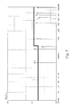
- Fig. 7 is a schematic diagram of an EMI testing result for a high-speed electrical connector without a shielding case.
- Fig. 8 is a schematic diagram of an EMI testing result for a high-speed electrical connector with a shielding case that is grounded by the contact method.
- Fig. 9 is a schematic diagram of an EMI testing result for a high-speed electrical connector with a shielding case that is grounded with a circuit board ground plane directly.
- the longitudinal axis is the radiated emission level
- the horizontal axis is the frequency value
- line A is the standard and regulation value.
- the intensity of the electromagnetic radiation cannot be above A.
- the intensity of the frequency b and c are radiated from the first connector. Compare and contrast the intensity of b and c frequencies of these three figures.
- the intensity of b and c frequencies in Fig. 7 are all above A.
- the intensity of b and c frequencies are all below A. Focusing on Fig. 9, the intensity of b and c frequency are not only below A, they are still much lower than A. It is known the EMI module of the embodiment prevents better shielding effect on the first connector.
- the shielding case caps on the high-speed connector and the shielding case grounded by connecting it to the ground plane of the circuit board with the protrusions can reduce the electromagnetic interference efficiently through the small return path.
- the shielding case is grounded by soldering it to the circuit board with at least one protrusion. Therefore, the EMI module prevents the shielding case has incomplete contact with the solder points and provides a better shielding design for the radiation source and provides a complete EMI protection for other electronic devices.
Landscapes
- Engineering & Computer Science (AREA)
- Microelectronics & Electronic Packaging (AREA)
- Physics & Mathematics (AREA)
- Electromagnetism (AREA)
- Shielding Devices Or Components To Electric Or Magnetic Fields (AREA)
Applications Claiming Priority (1)
| Application Number | Priority Date | Filing Date | Title |
|---|---|---|---|
| CNA2006100864593A CN101094584A (zh) | 2006-06-21 | 2006-06-21 | 电子组件屏蔽模块 |
Publications (2)
| Publication Number | Publication Date |
|---|---|
| EP1871157A2 true EP1871157A2 (fr) | 2007-12-26 |
| EP1871157A3 EP1871157A3 (fr) | 2009-12-09 |
Family
ID=38556960
Family Applications (1)
| Application Number | Title | Priority Date | Filing Date |
|---|---|---|---|
| EP07104681A Withdrawn EP1871157A3 (fr) | 2006-06-21 | 2007-03-22 | Module de protection EMI |
Country Status (2)
| Country | Link |
|---|---|
| EP (1) | EP1871157A3 (fr) |
| CN (1) | CN101094584A (fr) |
Cited By (1)
| Publication number | Priority date | Publication date | Assignee | Title |
|---|---|---|---|---|
| EP2355644A3 (fr) * | 2010-01-29 | 2011-10-05 | Fujitsu Limited | Structure de protection pour élément électronique et dispositif électronique |
Families Citing this family (1)
| Publication number | Priority date | Publication date | Assignee | Title |
|---|---|---|---|---|
| CN104144598B (zh) * | 2013-05-08 | 2018-02-02 | 鸿富锦精密工业(深圳)有限公司 | 屏蔽罩与电路板固定结构 |
Family Cites Families (3)
| Publication number | Priority date | Publication date | Assignee | Title |
|---|---|---|---|---|
| DE9318909U1 (de) * | 1993-12-09 | 1995-04-06 | GKR, Gesellschaft für Fahrzeugklimaregelung mbH, 71701 Schwieberdingen | Abschirmhaube für Schaltungsplatinen |
| DE19736208C1 (de) * | 1997-08-20 | 1998-12-10 | Siemens Ag | Schirmdichtung |
| TW200803714A (en) * | 2006-06-14 | 2008-01-01 | Asustek Comp Inc | Using mainboard grounded shielding device |
-
2006
- 2006-06-21 CN CNA2006100864593A patent/CN101094584A/zh active Pending
-
2007
- 2007-03-22 EP EP07104681A patent/EP1871157A3/fr not_active Withdrawn
Cited By (2)
| Publication number | Priority date | Publication date | Assignee | Title |
|---|---|---|---|---|
| EP2355644A3 (fr) * | 2010-01-29 | 2011-10-05 | Fujitsu Limited | Structure de protection pour élément électronique et dispositif électronique |
| US8797763B2 (en) | 2010-01-29 | 2014-08-05 | Fujitsu Limited | Shield structure for an electronic element and electronic device |
Also Published As
| Publication number | Publication date |
|---|---|
| EP1871157A3 (fr) | 2009-12-09 |
| CN101094584A (zh) | 2007-12-26 |
Similar Documents
| Publication | Publication Date | Title |
|---|---|---|
| US20070291464A1 (en) | EMI shielding module | |
| EP3060033B1 (fr) | Dispositif électronique | |
| US20090168386A1 (en) | Electronic apparatus and substrate mounting method | |
| US20090268420A1 (en) | Shielding assembly | |
| CN110998990B (zh) | 一种具有高屏蔽效率的电磁干扰笼罩和边框夹的收发器插座 | |
| US20110080721A1 (en) | Shield case and image display device | |
| US20040012939A1 (en) | EMI shielding apparatus | |
| US6660932B1 (en) | Dynamically moveable exhausting EMC sealing system | |
| AU2006301339A1 (en) | Electrical device | |
| US5635775A (en) | Printed circuit board mount electro-magnetic interference suppressor | |
| US6580028B1 (en) | EMI reduction device | |
| US6660933B2 (en) | Shielding element for electromagnetic shielding of an aperture opening | |
| US6116924A (en) | Electromagnetic emissions shielding structure for circuit board connector assembly | |
| EP1871157A2 (fr) | Module de protection EMI | |
| JPH11330771A (ja) | 低構造の無線周波数シ―ルド | |
| CN112423573B (zh) | 一种电磁防护装置 | |
| JP7514399B2 (ja) | 電子制御装置 | |
| JPH09232014A (ja) | インタフェースケーブル接続用コネクタ | |
| JP2012129495A (ja) | 通信機器のプリント回路基板の接地構造 | |
| KR900005306B1 (ko) | 전자 방해파의 발생을 저감한 전자장치 | |
| CA2562733A1 (fr) | Carte e/s de mise a la terre autonome | |
| JP2003508936A (ja) | Emi抑制配線プレートを備えた電気部品の組立体及びその製造方法並びにemi抑制配線プレート | |
| KR100577429B1 (ko) | 디스플레이 장치 | |
| US20260020205A1 (en) | Shielding combining press-fit with surface mount compression | |
| US10863615B2 (en) | Electronic apparatus |
Legal Events
| Date | Code | Title | Description |
|---|---|---|---|
| PUAI | Public reference made under article 153(3) epc to a published international application that has entered the european phase |
Free format text: ORIGINAL CODE: 0009012 |
|
| 17P | Request for examination filed |
Effective date: 20070709 |
|
| AK | Designated contracting states |
Kind code of ref document: A2 Designated state(s): AT BE BG CH CY CZ DE DK EE ES FI FR GB GR HU IE IS IT LI LT LU LV MC MT NL PL PT RO SE SI SK TR |
|
| AX | Request for extension of the european patent |
Extension state: AL BA HR MK YU |
|
| RAP1 | Party data changed (applicant data changed or rights of an application transferred) |
Owner name: ASUSTEK COMPUTER INC. |
|
| PUAL | Search report despatched |
Free format text: ORIGINAL CODE: 0009013 |
|
| AK | Designated contracting states |
Kind code of ref document: A3 Designated state(s): AT BE BG CH CY CZ DE DK EE ES FI FR GB GR HU IE IS IT LI LT LU LV MC MT NL PL PT RO SE SI SK TR |
|
| AX | Request for extension of the european patent |
Extension state: AL BA HR MK RS |
|
| AKY | No designation fees paid | ||
| STAA | Information on the status of an ep patent application or granted ep patent |
Free format text: STATUS: THE APPLICATION IS DEEMED TO BE WITHDRAWN |
|
| 18D | Application deemed to be withdrawn |
Effective date: 20100610 |
|
| REG | Reference to a national code |
Ref country code: DE Ref legal event code: 8566 |