EP1875608B1 - Circuit intégré assurant une fonctionnalité de commutation externe - Google Patents
Circuit intégré assurant une fonctionnalité de commutation externe Download PDFInfo
- Publication number
- EP1875608B1 EP1875608B1 EP06727709A EP06727709A EP1875608B1 EP 1875608 B1 EP1875608 B1 EP 1875608B1 EP 06727709 A EP06727709 A EP 06727709A EP 06727709 A EP06727709 A EP 06727709A EP 1875608 B1 EP1875608 B1 EP 1875608B1
- Authority
- EP
- European Patent Office
- Prior art keywords
- integrated circuit
- external
- contacts
- external contacts
- switching
- Prior art date
- Legal status (The legal status is an assumption and is not a legal conclusion. Google has not performed a legal analysis and makes no representation as to the accuracy of the status listed.)
- Expired - Lifetime
Links
Images


Classifications
-
- G—PHYSICS
- G06—COMPUTING OR CALCULATING; COUNTING
- G06K—GRAPHICAL DATA READING; PRESENTATION OF DATA; RECORD CARRIERS; HANDLING RECORD CARRIERS
- G06K19/00—Record carriers for use with machines and with at least a part designed to carry digital markings
- G06K19/06—Record carriers for use with machines and with at least a part designed to carry digital markings characterised by the kind of the digital marking, e.g. shape, nature, code
- G06K19/067—Record carriers with conductive marks, printed circuits or semiconductor circuit elements, e.g. credit or identity cards also with resonating or responding marks without active components
- G06K19/07—Record carriers with conductive marks, printed circuits or semiconductor circuit elements, e.g. credit or identity cards also with resonating or responding marks without active components with integrated circuit chips
- G06K19/0723—Record carriers with conductive marks, printed circuits or semiconductor circuit elements, e.g. credit or identity cards also with resonating or responding marks without active components with integrated circuit chips the record carrier comprising an arrangement for non-contact communication, e.g. wireless communication circuits on transponder cards, non-contact smart cards or RFIDs
-
- H—ELECTRICITY
- H03—ELECTRONIC CIRCUITRY
- H03K—PULSE TECHNIQUE
- H03K17/00—Electronic switching or gating, i.e. not by contact-making and –breaking
- H03K17/51—Electronic switching or gating, i.e. not by contact-making and –breaking characterised by the components used
- H03K17/56—Electronic switching or gating, i.e. not by contact-making and –breaking characterised by the components used by the use, as active elements, of semiconductor devices
- H03K17/687—Electronic switching or gating, i.e. not by contact-making and –breaking characterised by the components used by the use, as active elements, of semiconductor devices the devices being field-effect transistors
- H03K17/689—Electronic switching or gating, i.e. not by contact-making and –breaking characterised by the components used by the use, as active elements, of semiconductor devices the devices being field-effect transistors with galvanic isolation between the control circuit and the output circuit
-
- G—PHYSICS
- G06—COMPUTING OR CALCULATING; COUNTING
- G06K—GRAPHICAL DATA READING; PRESENTATION OF DATA; RECORD CARRIERS; HANDLING RECORD CARRIERS
- G06K19/00—Record carriers for use with machines and with at least a part designed to carry digital markings
- G06K19/06—Record carriers for use with machines and with at least a part designed to carry digital markings characterised by the kind of the digital marking, e.g. shape, nature, code
- G06K19/067—Record carriers with conductive marks, printed circuits or semiconductor circuit elements, e.g. credit or identity cards also with resonating or responding marks without active components
- G06K19/07—Record carriers with conductive marks, printed circuits or semiconductor circuit elements, e.g. credit or identity cards also with resonating or responding marks without active components with integrated circuit chips
- G06K19/0716—Record carriers with conductive marks, printed circuits or semiconductor circuit elements, e.g. credit or identity cards also with resonating or responding marks without active components with integrated circuit chips at least one of the integrated circuit chips comprising a sensor or an interface to a sensor
- G06K19/0717—Record carriers with conductive marks, printed circuits or semiconductor circuit elements, e.g. credit or identity cards also with resonating or responding marks without active components with integrated circuit chips at least one of the integrated circuit chips comprising a sensor or an interface to a sensor the sensor being capable of sensing environmental conditions such as temperature history or pressure
Definitions
- the present invention relates to an integrated circuit comprising a logic circuit and reception means for receiving external signals and for transmitting said received external signals to said logic circuit.
- the invention relates further to a device comprising such an integrated circuit and to methods of manufacturing and operating such an integrated circuit and for transmitting control data to a device.
- RFID Radio Frequency Identification
- a transponder normally includes a semiconductor chip for storing data, which may be programmable and rewritable, and an antenna being adapted for the relevant frequency band (e.g. US-UHF: 902 - 928 MHz, Europe: 863 - 868 MHz, ISM: 2.4 - 2.483 GHz).
- a common RFID system comprises RFID transponders, reading devices having a system antenna providing a bi-directional (data) communication between the transponders and the reading devices.
- Active transponders are provided with an energy supply of their own while passive transponders receive the power necessary for operation from the high frequency signals, which are also used for communication.
- US 2004/0131897 A1 discloses an RF transponder which combines the features of active and passive transponders.
- the transponder of US 2004/0131897 A1 comprises an electronic circuit, an RF antenna and a battery, wherein the electronic circuit is connected to the battery and thus receives energy from the battery upon reception of RF energy by the antenna which closes a switch between the electronic circuit and the battery and enables an electric connection between the battery and the electronic circuit.
- transponder systems are limited in their purpose since the transponders only provide a functionality of identification and data communication between the transponders and the reading devices.
- the first object according to the present invention is achieved by the integrated circuit as claimed in claim 1.
- the invention is based on the insight that an integrated circuit exhibits an extended functionality when provided with external contacts which are controlled by the integrated circuit, i.e. the functionality of a conventional transponder and an additional control functionality for controlling other devices by controlling an electrical connection between said external contacts.
- Controling an electrical connection i.e. the opening and closing of an electrical connection between contacts, is a process which is located within the integrated circuit and which is part of the abilities of an integrated circuit.
- the contacts between which the electrical connection is controlled are external contacts, the opening and closing of the electrical connection may directly influence a device connected to said external contacts.
- a number of conventional transponders comprise contacts for connection of the transponder antenna and normally two additional contacts.
- the additional contacts are connected to the logic circuit of the chip and used for testing the functioning of the semiconductor chip of the transponder, in particular of the logic circuit. This testing is normally conducted on wafer level, i.e. before the separation of the dice. To provide a power supply the test contacts may also be connected to the antenna contacts. After separation of the dice, i.e. cutting the wafer, the test contacts may remain on the transponder chip but are not further used. By providing mode altering means and at least two operation modes of the integrated circuit, these test contacts may be used for testing in one operation mode and as said external contacts in another operation mode, which allows an improved utilization of the space of the wafer and of the integrated circuit.
- said reception means are adapted for providing a power supply for said integrated circuit, utilizing energy from said external signals.
- the external signals are essential for the input of data into the integrated circuit. Since the switching means are controlled in response to said external signals, these signals may also be used as a power source.
- the integrated circuit of another embodiment further comprises identification means including a substantially unique identifier, wherein said logic circuit controls said switching means in response only to received external signals which correspond to said unique identifier.
- identification means including a substantially unique identifier
- said logic circuit controls said switching means in response only to received external signals which correspond to said unique identifier.
- said reception means are adapted for receiving electro-magnetic signals, in particular radio frequency signals.
- Said integrated circuit including such reception means may form a transponder, in particular an RF-transponder, which exhibits an extended functionality and may nevertheless be incorporated into known communication systems, in particular RF communication systems.
- said logic circuit comprises coding means for controlling said switching means for a sequence of switching operations in order to generate a code signal.
- a sequence of switching operations forms a sequence of such changes between states and may thus be used to transmit data in the form of a binary code signal.
- sequence of switching operations also includes the case of only one switching operation, i.e. the switching from one state to another state.
- switching and switching operations in the present context, since there may be provided more states of electrical connection between said contacts than just the two on and off states.
- said switching means are controlled by said coding means to provide a change of the electrical resistance of the electrical connection between said external contacts between a low (or even very low) value (corresponding to a completely closed connection or on-state) and a high (or even infinite) value (corresponding to an open connection or off-state) in discrete steps or continuously.
- voltages having different values and thus forming a code signal may be outputted upon control of said coding means, for example for addressing an external A/D-converter connected to said external contacts.
- said logic circuit comprises input detection means for detecting an external electronic signal applied to said external contacts.
- the external contacts of this embodiment are used as an interface to and from the logic circuit.
- the external electronic signal applied to said external contacts may, for example, be used to re-program the logic circuit, to alter the above-mentioned unique identifier or for other data input into the integrated circuit.
- the applied electronic signal may be of any kind including a binary signal, i.e. a sequence of high and low signals, and analog signals like the ones provided by analog sensors, e.g. a temperature sensor, or by an external D/A-converter.
- the object of the present invention is moreover achieved by a method for operating an integrated circuit as claimed in claim 13.
- An embodiment of the method of operating the integrated circuit further comprises further steps in accordance with claim 15.
- Yet another solution of the object of the invention is a method for manufacturing an integrated circuit as claimed in claim 14.
- Fig. 1 shows a basic circuitry of a known integrated circuit 12 comprising antenna contact pads 14a, 14b for connecting an external antenna to said integrated circuit 12 to form an RF transponder.
- Said integrated circuit 12 further includes test contact pads 16a, 16b for providing a functionality for testing said integrated circuit 12.
- Said integrated circuit 12 is manufactured together with other integrated circuits (not shown) on a wafer (not shown). On the wafer a number of integrated circuits are arranged, while between the integrated circuits some space is left unoccupied. For separation of the integrated circuits the wafer is cut after forming the integrated circuits on the wafer and after testing of the integrated circuits.
- test contact pads 16a, 16b are electrically connected to the antenna contact pads 14a, 14b via contact lines 18a, 18b, respectively, which are arranged on the wafer mostly outside the area of the integrated circuit 12.
- contact lines 18a, 18b are interrupted, leaving the test contact pads 16a, 16b without further use.
- Said integrated circuit 12 further comprises a logic circuit 20 which is electrically connected to the antenna contact pads 14a, 14b.
- a capacitor 22 and a resistor 24 are arranged in parallel withthe logic circuit 20.
- a rectifier 26 is provided in the connection between the logic circuit 20 and antenna contact pad 14b.
- Rectifier 26 resistor 24 and capacitor 22 form a rectifying circuit 28 for rectifying the electromagnetic signals received by an antenna (not shown) in order to provide a DC voltage for the operation of the integrated circuit 12.
- the resistor 24 may be replaced by a transistor, and the rectifying circuit 28 may be replaced by some different means for providing a power supply for the integrated circuit 12. This also applies to the embodiments according to the present invention described below.
- Fig. 2 shows a basic circuitry of a first embodiment of an integrated circuit 30 according to the present invention.
- Said integrated circuit 30 comprises two antenna pads 32a, 32b, a rectifying circuit 34 including a rectifier 36, a capacitor 38, and a resistor 40 (or transistor) and a logic circuit 42 which is connected to said antenna pads 32a, 32b via said rectifying circuit 34 in a manner similar to the known integrated circuit 12 shown in Fig. 1 .
- said integrated circuit 30 is provided with two external contacts 44a, 44b which are connected to said logic circuit 42 and to one antenna pad 32a via switching means 46 comprising two resistors 48, 50 and a transistor element 52, i.e. a MOSFET.
- Said logic circuit 42 is coupled to the gate electrode of the transistor element 52 while the drain electrode and the source electrode are coupled to the external contacts 44a, 44b, respectively.
- the resistors 48, 50 are provided to prevent overloading of the transistor element 52, for example if there is a shortcut between the two external contacts 44a, 44b.
- said logic circuit 42 controls an electrical connection between said two external contacts 44a, 44b.
- To provide such a switching functionality use can be made of many possible wirings known to one skilled in the art, so it will be understood that the embodiment is illustrated only by way of example in Fig. 2 . Further, there are other possible ways to provide a desired switching functionality including using other kinds of transistor elements, a microelectromechanical switch and/or a piezoelectric microelectromechanical switch.
- Fig. 3 shows a basic circuitry of a second embodiment of an integrated circuit 54 according to the present invention.
- Said integrated circuit 54 of the second embodiment corresponds in many parts to the integrated circuit 30 of the first embodiment shown in Fig. 2 .
- said integrated circuit 54 of the second embodiment comprises an electrical coupling 56 between said external contact 44b and said logic circuit 42.
- said electrical coupling 56 Assuming the electrical connection between the external contacts 44a, 44b is closed and said external contact 44b is provided with a low signal via the transistor element 52, a high signal provided by an external element to said external contact 44b is detected by said logic circuit 42.
- other possible ways of providing an input via said external contacts 44a, 44b and detection of said input by said logic circuit 42 are known to one skilled in the art.
- contact lines similar to the contact lines 18a, 18b of the known integrated circuit 12 shown in Fig. 1 are provided between said external contacts 44a, 44b and said antenna pads 32a, 32b for allowing a testing process of the integrated circuit 54 in a manner similar to a common testing process.
- Fig. 4 shows the logic circuit 42 according to the present invention in greater detail.
- Said logic circuit 42 is provided with mode altering means 58 for alternating between a first mode for providing a switching functionality through said external contacts 44a, 44b and a second operation mode for performing a functionality test of the integrated circuit 30, 54 by means of said external contacts 44a, 44b.
- Said logic circuit 42 is further provided with identification means 60 which include an identifier. Said identifier, for example a binary number, is substantially unique and used to substantially uniquely identify said logic circuit 42 and thus said integrated circuit 30, 54.
- Said logic circuit 42 includes coding means 62 for generating a sequence of switching commands forming a code signal and input detection means 64 for detecting an external electronic signal (e.g. binary or of special amplitude) via said electrical coupling 56.
- the mode altering means 58 may also be arranged on the waver outside of the area of the integrated circuit 30, 54 and also separated from the integrated circuit 30, 54 during the separation of the dice, since it is not necessary to change between the different operation modes of switching and testing again once the integrated circuit 30, 54 has been tested successfully.
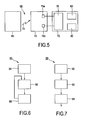
- Fig. 5 shows a block diagram illustrating a system 66 comprising a control unit 68, an integrated circuit 70 and a device 72 to be controlled according to the invention.
- Said control unit 68 is provided with means for generating and transmitting control signals.
- Said integrated circuit 70 is adapted for receiving transmitted signals and provided with two external contacts 76a, 76b.
- Said device 72 which is to be controlled according to said control signals, is coupled to said external contacts 76a, 76b and provided with a function circuitry 78 to be controlled
- An example of said device 72 is a TV set which may be switched on and off by means of said integrated circuit 70.
- the switching functionality of said integrated circuit 70 is used to implement an alternative to the common standby function of known TV sets.
- Said device 72 further includes output detection means 80 for detecting a sequence of switching operations of the electrical connection between said external contacts 76a, 76b and signal means 82 for applying an electronic signal to said external contacts 76a, 76b.
- Said control unit 68 transmits control data using - for example - electro-magnetic signals, in particular radio frequency signals 74, to said integrated circuit 70 which receives said signals 74 and processes said signals 74 to generate a sequence of switching operations of an electrical connection between two external contacts 76a, 76b of said integrated circuit 70. Said sequence of switching operations is detected by said output detection means 80 of said device 72 and said function circuitry 78 is controlled accordingly.
- said device 72 may apply an electronic signal to said external contacts 76a, 76b by means of said signal means 82, for example, to acknowledge a control operation of said function circuitry 78 to said integrated circuit 70.
- the device 72 also can be a single external component such as e.g. a sensor sensing one and/or more physical parameters such as e.g. the temperature and/or humidity and/or pressure etc. of the environment the sensor (and possibly also the transponder) is located in.
- a DC-signal (or AC-Signal) of special amplitude, generated by the sensor device can be detected by the transponder. This information can be sent to the reader device in order to allow the control of physical parameters.
- a power element for increasing the current / voltage which is switched by the electrical connection between said external contacts 76a, 76b.
- the power element is controlled by the switching of said connection, and the power element itself then switches an electrical connection capable of an increased current and/or voltage.
- the invention is described with two antenna contacts 32a, 32b and two external contacts 44a, 44b, 76a, 76b, the invention is not limited to this number of contacts. It is possible to provide a different number of antenna contacts 32a, 32b, including only one antenna contact for a monopole antenna and a greater number of external contacts 44a, 44b, 76a, 76b.
- Fig. 6 shows a block diagram of a method 83 for operating an integrated circuit 30, 54, 70 according to the present invention.
- a first step 84 an integrated circuit 30, 54, 70 is provided with a first operation mode having a switching functionality in regard to an electrical connection between two external contacts 44a, 44b, 76a, 76b of said integrated circuit 30, 54, 70.
- Step 84 is followed by step 86 of said integrated circuit 30, 54, 70 receiving external signals.
- switching means 46 of said integrated circuit 30, 54, 70 are controlled to perform a switching operation of said electrical connection in step 88 which may be followed by step 86 again.
- Fig. 7 shows a block diagram of a method 89 for manufacturing an integrated circuit 30, 54, 70 according to the present invention comprising a logic circuit 42, at least two external contacts 44a, 44b, 76a, 76b, switching means 46 connecting said logic circuit 42 to said external contacts 44a, 44b, 76a, 76b, reception means 34 for receiving external signals and for transmitting said received external signals to said logic circuit 42 and mode altering means 58 for alternating between at least two operation modes of said integrated circuit 30, 54, 70.
- the method comprises the steps of producing 90 said integrated circuit 30, 54, 70 being in a second operation mode followed by testing 92 said logic circuit 42 by means of said external contacts 44a, 44b, 76a, 76b.
- said integrated circuit 30, 54, 70 is changed 94 to a first operation mode for providing a switching functionality using said external contacts 44a, 44b, 76a, 76b.
- Fig. 8 shows a block diagram of a method 95 for transmitting control data by means of an integrated circuit 30, 54, 70 according to the present invention.
- Control data is transmitted in step 96 as external signals to an integrated circuit 30, 54, 70 according to the present invention, which is coupled via said external contacts 44a, 44b, 76a, 76b to a device 72 to be controlled.
- said switching means 46 are controlled by said logic circuit 42 in order to generate a sequence of switching operations representing said control data, for example, in binary or analog form.
- step 100 following step 98 said sequence of switching operations is detected by said device 72 via said external contacts 44a, 44b, 76a, 76b.
- Step 100 may be followed by step 96 for transmitting the next control data or by step 98 for generating another sequence of switching operations.
- Additional external contacts 44a, 44b, 76a, 76b are used to provide a switching functionality, so that the integrated circuit 30, 54, 70 can be used to control other devices, for example, to activate and deactivate other devices.
Landscapes
- Engineering & Computer Science (AREA)
- Computer Hardware Design (AREA)
- Microelectronics & Electronic Packaging (AREA)
- Physics & Mathematics (AREA)
- General Physics & Mathematics (AREA)
- Theoretical Computer Science (AREA)
- Computer Networks & Wireless Communication (AREA)
- Semiconductor Integrated Circuits (AREA)
- Tests Of Electronic Circuits (AREA)
- Credit Cards Or The Like (AREA)
Claims (15)
- Circuit intégré (30, 54, 70) comprenant :un circuit logique (42),des contacts d'antenne (32a, 32b) pour connecter une antenne externe audit circuit intégré (30, 54, 70) afin de former un transpondeur RF,au moins deux contacts externes (44a, 44b, 76a, 76b), dan lequel lesdits contacts externes (44a, 44b, 76a, 76b) sont configurés en vue de tester la fonctionnalité du circuit intégré (30, 54, 70) au niveau plaquette,des moyens de commutation (46) connectant ledit circuit logique (42) aux dits contacts externes (44a, 44b, 76a, 76b), etdes moyens de réception (34) pour recevoir des signaux externes par l'intermédiaire des contacts d'antenne (32a, 32b), et pour transmettre lesdits signaux externes reçus audit circuit logique (42),dans lequel ledit circuit intégré (30, 54, 70) est exploitable dans un premier mode de fonctionnement pour fournir une fonctionnalité de commutation à travers lesdits contacts externes (44a, 44b, 76a, 76b) par l'intermédiaire desdits moyens de commutation (46) pour commuter une connexion électrique entre lesdits contacts externes (44a, 44b, 76a, 76b) afin d'obtenir une fonctionnalité de commande supplémentaire pour commander un dispositif (72) à commander en contrôlant la connexion électrique entre lesdits contacts externes (44a, 44b, 76a, 76b), dans lequel lesdits moyens de commutation (46) sont commandés par ledit circuit logique (42) en réponse aux dits signaux externes reçus, et dans lequel lesdits contacts externes( 44a, 44b, 76a, 46b) sont adaptés pour être connectés au dispositif (72) à commander,
dans lequel le circuit intégré comprend, de plus, des moyens de modification de mode (58) pour opérer un changement entre au moins deux modes de fonctionnement dudit circuit intégré (30, 54, 70), les au moins deux modes de fonctionnement comprenant le premier mode de fonctionnement et un second mode de fonctionnement destiné à exécuter un test de fonctionnalité dudit circuit intégré (30, 54, 70) au moyen desdits contacts externes (44a, 44b, 76a, 76b). - Circuit intégré (30, 54, 70) selon la revendication 1,
dans lequel lesdits moyens de réception (34) sont adaptés pour fournir une alimentation électrique destinée audit circuit intégré (30, 54, 70)en utilisant une énergie provenant desdits signaux externes. - Circuit intégré (30, 54, 70) selon la revendication 1, comprenant, de plus, des moyens d'indentification (60) incluant un identificateur essentiellement unique, dans lequel ledit circuit logique (42) commande lesdits moyens de commutation (46) en réponse seulement aux signaux externes reçus qui correspondent audit identificateur unique.
- Circuit intégré (30, 54, 70) selon la revendication 1, dans lequel lesdits moyens de réception (34) sont adaptés pour recevoir des signaux électromagnétiques, en particulier, des signaux de fréquence radioélectrique.
- Circuit intégré (30, 54, 70) selon la revendication 1, dans lequel ledit circuit logique (42) comporte des moyens de codage (62) destinés à commander lesdits moyens de commutation (46) pour une séquence d'opérations de commutation afin de générer un signal de code.
- Circuit intégré (30, 54, 70) selon la revendication 5, dans lequel ledit signal de code généré est un signal binaire ou un signal analogique.
- Circuit intégré (30, 54, 70) selon la revendication 1, dans lequel ledit circuit logique (42) comporte des moyens de détection d'entrée (64) pour détecter un signal électronique externe appliqué aux dits contacts externes (44a, 44b, 76a, 76b).
- Circuit intégré (30, 54, 70) selon la revendication 1, dans lequel ledit circuit intégré (30, 54, 70) fait partie d'un transpondeur d'indentification à fréquence radioélectrique.
- Circuit intégré (30, 54, 70) selon la revendication 1, dans lequel lesdits moyens de commutation (46) comprennent un transistor (52), un micro-commutateur électromécanique et/ou un micro-commutateur électromécanique piézoélectrique.
- Système comprenant un circuit intégré (30, 54, 70) selon la revendication 1 et un dispositif (72) couplé au circuit intégré (30, 54, 70), dans lequel le dispositif (72) comprend une circuiterie fonctionnelle (78) et dans lequel ladite circuiterie fonctionnelle (78) est connectée aux dits contacts externes (44a, 44b, 76a, 76b) dudit circuit intégré (30, 54, 70) qui commande ladite circuiterie fonctionnelle (78) à l'aide desdits moyens de commutation (46) dans ledit premier mode de fonctionnement.
- Système selon la revendication 10, dans lequel ledit dispositif (72) comprend, de plus, des moyens de détection de sortie (80) pour détecter ladite séquence desdites opérations de commutation formant un signal de code.
- Système selon la revendication 10 dans lequel ledit dispositif (72) comprend, de plus, des moyens de signaux (82) pour appliquer un signal électronique aux dits contacts externes.
- Procédé (83) pour rendre opérationnel un circuit intégré (30, 54, 70) comprenant un circuit logique (42), des contacts d'antenne (32a, 32b) permettant de connecter une antenne externe audit circuit intégré (30, 54, 70) en vue de former un transpondeur RF, au moins deux contacts externes (44a, 44b, 76a, 76b), dans lequel lesdits contacts externes (44a, 44b, 76a, 76b) sont configurés en vue de tester la fonctionnalité du circuit intégré (30, 54, 70) au niveau plaquette, des moyens de commutation (46) connectant ledit circuit logique (42) aux dits contacts externes (44a, 44b, 76a, 76b), lesquels sont adaptés pour être connectés à un dispositif (72) à commander, et des moyens de réception (34) permettant de recevoir des signaux externes par l'intermédiaire des contacts d'antenne (32a, 32b) et de transmettre lesdits signaux externes reçus audit circuit logique (42), dans lequel le circuit intégré comprend, de plus, des moyens de modification de mode (58) permettant un changement entre au moins deux modes de fonctionnement dudit circuit intégré (30, 54, 70), les, au moins deux, modes de fonctionnement comprenant un premier mode de fonctionnement et un second mode de fonctionnement pour exécuter un test de fonctionnalité dudit circuit intégré (30, 54, 70) au moyen desdits contacts externes (44a, 44b, 76a, 76b), le procédé consistant à :- fournir (84) le premier mode de fonctionnement afin de fournir une fonctionnalité de commutation par l'intermédiaire desdits contacts externes (44a, 44b, 76a, 76b) à l'aide desdits moyens de commutation (46) en vue de commuter une connexion électrique entre lesdits contacts externes (44a, 44b, 76a, 76b) pour obtenir une fonctionnalité de commande supplémentaire pour commander le dispositif (72) à commander en contrôlant la connexion électrique entre lesdits contacts externes (44a, 44b, 76a, 76b),- recevoir (86) lesdits signaux externes et transmettre lesdits signaux externes audit circuit logique (42) à l'aide desdits moyens de réception (34), et- commander (88) lesdits moyens de commutation (46) par l'intermédiaire dudit circuit logique (42) en réponse aux dits signaux externes reçus.
- Procédé (89) de fabrication d'un circuit intégré (30, 54, 70) comprenant un circuit logique (42) des contacts d'antenne (32a, 32b) permettant de connecter une antenne externe audit circuit intégré (30, 54, 70) afin de former un transpondeur RF, au moins deux contacts externes (44a, 44b, 76a, 76b), dans lequel lesdits contacts externes (44a, 44b, 76a, 76b) sont configurés en vue de tester la fonctionnalité du circuit intégré (30, 50, 70) au niveau plaquette, des moyens de commutation (46) connectant ledit circuit logique (42) aux dits contacts externes (44a, 44b, 76a, 76b), lesquels sont adaptés pour être connectés à un dispositif (72) à commander, des moyens de réception (34) destinés à recevoir des signaux externes par l'intermédiaire des contacts d'antenne (32a, 32b) et à transmettre lesdits signaux externes reçus audit circuit logique (42) et des moyens de modification de mode (58) pour opérer un changement entre au moins deux modes de fonctionnement dudit circuit intégré (30, 54, 70), les au moins deux modes de fonctionnement comprenant un premier mode de fonctionnement et un second mode de fonctionnement pour exécuter un test de fonctionnalité dudit circuit intégré (30, 54, 70) au moyen desdits contacts externes (44a, 44b, 76a, 76b), le procédé consistant à :- réaliser (90) ledit circuit intégré dans le second mode de fonctionnement,- tester (92) ledit circuit logique (42) au moyen desdits contacts externes (44a, 44b, 76a, 76b), et- faire passer (94) ledit circuit intégré (30, 54, 70) dans le premier mode de fonctionnement,dans lequel ledit circuit logique (42) commande lesdits moyens de commutation (46) pour fournir une fonctionnalité de commutation par l'intermédiaire desdits contacts externes (44a, 44b, 76a, 76b) à l'aide desdits moyens de commutation (46) pour commuter une connexion électrique entre lesdits contacts externes (44a, 44b, 76a, 76b) afin d'obtenir une fonctionnalité de commande supplémentaire pour commander le dispositif (72) à commander en contrôlant la connexion électrique entre lesdits contacts externes (44a, 44b, 76a, 76b) dans ledit premier mode de fonctionnement dudit circuit intégré (30, 54, 70) en réponse aux dits signaux externes reçus.
- Procédé (95) selon la revendication 13, consistant, de plus, à :- transmettre (96) des données de commande sous la forme desdits signaux externes au circuit intégré (30, 54, 70),- dans lequel commander (98) lesdits moyens de commutation (46) par l'intermédiaire dudit circuit logique (42) consiste à générer une séquence d'opérations de commutation représentant lesdites données de commande, et- détecter (100) ladite séquence d'opérations de commutation par l'intermédiaire dudit dispositif (72) au moyen desdits contacts externes (44a, 44b, 76a, 76b).
Priority Applications (1)
| Application Number | Priority Date | Filing Date | Title |
|---|---|---|---|
| EP06727709A EP1875608B1 (fr) | 2005-03-30 | 2006-03-22 | Circuit intégré assurant une fonctionnalité de commutation externe |
Applications Claiming Priority (3)
| Application Number | Priority Date | Filing Date | Title |
|---|---|---|---|
| EP05102495 | 2005-03-30 | ||
| EP06727709A EP1875608B1 (fr) | 2005-03-30 | 2006-03-22 | Circuit intégré assurant une fonctionnalité de commutation externe |
| PCT/IB2006/050882 WO2006103599A1 (fr) | 2005-03-30 | 2006-03-22 | Circuit intégré assurant une fonctionnalité de commutation externe |
Publications (2)
| Publication Number | Publication Date |
|---|---|
| EP1875608A1 EP1875608A1 (fr) | 2008-01-09 |
| EP1875608B1 true EP1875608B1 (fr) | 2009-12-30 |
Family
ID=36636876
Family Applications (1)
| Application Number | Title | Priority Date | Filing Date |
|---|---|---|---|
| EP06727709A Expired - Lifetime EP1875608B1 (fr) | 2005-03-30 | 2006-03-22 | Circuit intégré assurant une fonctionnalité de commutation externe |
Country Status (9)
| Country | Link |
|---|---|
| US (1) | US9058549B2 (fr) |
| EP (1) | EP1875608B1 (fr) |
| JP (1) | JP2008535234A (fr) |
| KR (1) | KR20070116168A (fr) |
| CN (1) | CN101167252B (fr) |
| AT (1) | ATE453958T1 (fr) |
| DE (1) | DE602006011454D1 (fr) |
| TW (1) | TW200731668A (fr) |
| WO (1) | WO2006103599A1 (fr) |
Families Citing this family (4)
| Publication number | Priority date | Publication date | Assignee | Title |
|---|---|---|---|---|
| JP6147713B2 (ja) * | 2014-09-26 | 2017-06-14 | 日本電信電話株式会社 | Rfidタグ、その出荷前管理システム、出荷前管理方法 |
| KR102312630B1 (ko) | 2014-09-30 | 2021-10-18 | 삼성전자주식회사 | 반도체 패키지 및 그 제조방법 |
| US11106965B2 (en) * | 2019-08-28 | 2021-08-31 | Electronics And Telecommunications Research Institute | Radio frequency identification tag and manufacturing method thereof |
| CN111181345B (zh) * | 2020-01-10 | 2021-01-15 | 无锡泽太微电子有限公司 | 机电能量收集控制电路和控制方法 |
Family Cites Families (15)
| Publication number | Priority date | Publication date | Assignee | Title |
|---|---|---|---|---|
| US2968802A (en) * | 1957-04-26 | 1961-01-17 | Rca Corp | Radio signal receiving system |
| US4857893A (en) * | 1986-07-18 | 1989-08-15 | Bi Inc. | Single chip transponder device |
| AT395224B (de) * | 1990-08-23 | 1992-10-27 | Mikron Ges Fuer Integrierte Mi | Kontaktloses, induktives datenuebertragungssystem |
| JP3100716B2 (ja) * | 1991-01-04 | 2000-10-23 | シーエスアイアール | 識別装置 |
| JPH0962816A (ja) * | 1994-10-06 | 1997-03-07 | Mitsubishi Electric Corp | 非接触icカードおよびこれを含む非接触icカードシステム |
| FR2735597B1 (fr) | 1995-06-14 | 1997-08-29 | Solaic Sa | Carte electronique comportant un interrupteur deplacable en translation |
| US5874902A (en) * | 1996-07-29 | 1999-02-23 | International Business Machines Corporation | Radio frequency identification transponder with electronic circuit enabling/disabling capability |
| FR2752076B1 (fr) * | 1996-08-05 | 1998-09-11 | Inside Technologies | Systeme d'alimentation electrique pour microcircuit a fonctionnement mixte, avec ou sans contact |
| US5963144A (en) * | 1997-05-30 | 1999-10-05 | Single Chip Systems Corp. | Cloaking circuit for use in a radiofrequency identification and method of cloaking RFID tags to increase interrogation reliability |
| DE69900584T3 (de) * | 1998-07-21 | 2009-05-20 | Nxp B.V. | System zur übertragung von daten von einem datenträger nach einer station mittels eines oder zum mindest eines anderen hilfsträgersignals |
| WO2000045595A1 (fr) * | 1999-01-27 | 2000-08-03 | Viktor Petrovich Kandidatov | Dispositif permettant d'allumer et d'eteindre un appareil electrique a distance |
| US6634565B2 (en) | 2001-11-06 | 2003-10-21 | Litronic, Inc. | Smart card having additional connector pads |
| TW572502U (en) | 2002-12-18 | 2004-01-11 | C One Technology Corp | Small electronic card capable of changing the communication device |
| US7603144B2 (en) * | 2003-01-02 | 2009-10-13 | Cymbet Corporation | Active wireless tagging system on peel and stick substrate |
| CN2624522Y (zh) * | 2003-06-04 | 2004-07-07 | 侯康 | 一种感应触发式电视机背光灯 |
-
2006
- 2006-03-22 CN CN2006800101665A patent/CN101167252B/zh not_active Expired - Fee Related
- 2006-03-22 US US11/910,182 patent/US9058549B2/en active Active
- 2006-03-22 KR KR1020077024967A patent/KR20070116168A/ko not_active Withdrawn
- 2006-03-22 DE DE602006011454T patent/DE602006011454D1/de not_active Expired - Lifetime
- 2006-03-22 EP EP06727709A patent/EP1875608B1/fr not_active Expired - Lifetime
- 2006-03-22 WO PCT/IB2006/050882 patent/WO2006103599A1/fr not_active Ceased
- 2006-03-22 AT AT06727709T patent/ATE453958T1/de not_active IP Right Cessation
- 2006-03-22 JP JP2008503646A patent/JP2008535234A/ja not_active Withdrawn
- 2006-03-27 TW TW095110603A patent/TW200731668A/zh unknown
Also Published As
| Publication number | Publication date |
|---|---|
| CN101167252B (zh) | 2010-12-22 |
| WO2006103599A1 (fr) | 2006-10-05 |
| DE602006011454D1 (de) | 2010-02-11 |
| KR20070116168A (ko) | 2007-12-06 |
| TW200731668A (en) | 2007-08-16 |
| CN101167252A (zh) | 2008-04-23 |
| ATE453958T1 (de) | 2010-01-15 |
| US9058549B2 (en) | 2015-06-16 |
| JP2008535234A (ja) | 2008-08-28 |
| EP1875608A1 (fr) | 2008-01-09 |
| US20080272893A1 (en) | 2008-11-06 |
Similar Documents
| Publication | Publication Date | Title |
|---|---|---|
| US20090303013A1 (en) | Systems and methods for wireless control of equipment | |
| US10430622B2 (en) | RFID tag with reconfigurable properties and/or reconfiguring capability | |
| US20230281404A1 (en) | Systems and Methods to Selectively Connect Antennas to Communicate via Radio Frequency Signals | |
| US6118189A (en) | Identification system reader with multiplexed antennas | |
| US7535362B2 (en) | Circuit arrangement and method for supplying power to a transponder | |
| US7762471B2 (en) | Proximity payment card with cost-effective connection between user-actuatable input switch and RFID IC | |
| WO2005034010A2 (fr) | Systeme couple de radiofrequence electrique, reparti | |
| EP2005401A2 (fr) | Procedes et systemes permettant de tester des etiquettes d'identification de radiofrequence (rfid) ayant de multiples antennes | |
| JP2004357300A (ja) | 後方散乱ベースのトランスポンダのための位相変調回路 | |
| US7400250B2 (en) | Indicating radio frequency identification (RF-ID) tag | |
| US7746216B2 (en) | Method and circuit arrangement for holding a control state during inadequate power supply in an RF transponder or remote sensor | |
| US20100290368A1 (en) | Half-duplex rfid transponder and a method of operating a half-duplex rfid transponder | |
| EP4411593A3 (fr) | Étiquette électronique | |
| EP1875608B1 (fr) | Circuit intégré assurant une fonctionnalité de commutation externe | |
| US20040147281A1 (en) | Transmitter and receiver circuits with controller-less operation capability | |
| EP2239688B1 (fr) | Dispositif RFID pouvant fonctionner dans un premier et un deuxième état de fonctionnement | |
| KR100390964B1 (ko) | 데이터 처리 장치와 데이터 처리 장치의 동작 제어 방법 | |
| US8957766B2 (en) | Universal transmitter | |
| CN101341416B (zh) | 具有射频接口的电路和数据载体 | |
| WO2020213679A1 (fr) | Système de transmission, antenne, dispositif de commande, et procédé de transmission | |
| US20100214081A1 (en) | Unidirectional active electronic tag and method for setting parameters thereof | |
| US20110173424A1 (en) | Integrated circuit device configuration | |
| JP2004012463A (ja) | デバイス署名情報を使用したパファーマンスチューニング | |
| KR100748600B1 (ko) | 알에프아이디 센서 | |
| WO2025136935A1 (fr) | Inventoriage d'étiquettes basé sur des drapeaux mis en correspondance en mémoire |
Legal Events
| Date | Code | Title | Description |
|---|---|---|---|
| PUAI | Public reference made under article 153(3) epc to a published international application that has entered the european phase |
Free format text: ORIGINAL CODE: 0009012 |
|
| 17P | Request for examination filed |
Effective date: 20071030 |
|
| AK | Designated contracting states |
Kind code of ref document: A1 Designated state(s): AT BE BG CH CY CZ DE DK EE ES FI FR GB GR HU IE IS IT LI LT LU LV MC NL PL PT RO SE SI SK TR |
|
| AX | Request for extension of the european patent |
Extension state: AL BA HR MK YU |
|
| 17Q | First examination report despatched |
Effective date: 20080130 |
|
| GRAP | Despatch of communication of intention to grant a patent |
Free format text: ORIGINAL CODE: EPIDOSNIGR1 |
|
| GRAS | Grant fee paid |
Free format text: ORIGINAL CODE: EPIDOSNIGR3 |
|
| GRAA | (expected) grant |
Free format text: ORIGINAL CODE: 0009210 |
|
| AK | Designated contracting states |
Kind code of ref document: B1 Designated state(s): AT BE BG CH CY CZ DE DK EE ES FI FR GB GR HU IE IS IT LI LT LU LV MC NL PL PT RO SE SI SK TR |
|
| AX | Request for extension of the european patent |
Extension state: AL BA HR MK YU |
|
| REG | Reference to a national code |
Ref country code: GB Ref legal event code: FG4D |
|
| REG | Reference to a national code |
Ref country code: CH Ref legal event code: EP |
|
| REG | Reference to a national code |
Ref country code: IE Ref legal event code: FG4D |
|
| REF | Corresponds to: |
Ref document number: 602006011454 Country of ref document: DE Date of ref document: 20100211 Kind code of ref document: P |
|
| PG25 | Lapsed in a contracting state [announced via postgrant information from national office to epo] |
Ref country code: FI Free format text: LAPSE BECAUSE OF FAILURE TO SUBMIT A TRANSLATION OF THE DESCRIPTION OR TO PAY THE FEE WITHIN THE PRESCRIBED TIME-LIMIT Effective date: 20091230 Ref country code: LT Free format text: LAPSE BECAUSE OF FAILURE TO SUBMIT A TRANSLATION OF THE DESCRIPTION OR TO PAY THE FEE WITHIN THE PRESCRIBED TIME-LIMIT Effective date: 20091230 Ref country code: SE Free format text: LAPSE BECAUSE OF FAILURE TO SUBMIT A TRANSLATION OF THE DESCRIPTION OR TO PAY THE FEE WITHIN THE PRESCRIBED TIME-LIMIT Effective date: 20091230 |
|
| REG | Reference to a national code |
Ref country code: NL Ref legal event code: VDEP Effective date: 20091230 |
|
| LTIE | Lt: invalidation of european patent or patent extension |
Effective date: 20091230 |
|
| PG25 | Lapsed in a contracting state [announced via postgrant information from national office to epo] |
Ref country code: SI Free format text: LAPSE BECAUSE OF FAILURE TO SUBMIT A TRANSLATION OF THE DESCRIPTION OR TO PAY THE FEE WITHIN THE PRESCRIBED TIME-LIMIT Effective date: 20091230 Ref country code: PL Free format text: LAPSE BECAUSE OF FAILURE TO SUBMIT A TRANSLATION OF THE DESCRIPTION OR TO PAY THE FEE WITHIN THE PRESCRIBED TIME-LIMIT Effective date: 20091230 Ref country code: LV Free format text: LAPSE BECAUSE OF FAILURE TO SUBMIT A TRANSLATION OF THE DESCRIPTION OR TO PAY THE FEE WITHIN THE PRESCRIBED TIME-LIMIT Effective date: 20091230 |
|
| PG25 | Lapsed in a contracting state [announced via postgrant information from national office to epo] |
Ref country code: AT Free format text: LAPSE BECAUSE OF FAILURE TO SUBMIT A TRANSLATION OF THE DESCRIPTION OR TO PAY THE FEE WITHIN THE PRESCRIBED TIME-LIMIT Effective date: 20091230 |
|
| PG25 | Lapsed in a contracting state [announced via postgrant information from national office to epo] |
Ref country code: RO Free format text: LAPSE BECAUSE OF FAILURE TO SUBMIT A TRANSLATION OF THE DESCRIPTION OR TO PAY THE FEE WITHIN THE PRESCRIBED TIME-LIMIT Effective date: 20091230 Ref country code: IS Free format text: LAPSE BECAUSE OF FAILURE TO SUBMIT A TRANSLATION OF THE DESCRIPTION OR TO PAY THE FEE WITHIN THE PRESCRIBED TIME-LIMIT Effective date: 20100430 Ref country code: ES Free format text: LAPSE BECAUSE OF FAILURE TO SUBMIT A TRANSLATION OF THE DESCRIPTION OR TO PAY THE FEE WITHIN THE PRESCRIBED TIME-LIMIT Effective date: 20100410 Ref country code: NL Free format text: LAPSE BECAUSE OF FAILURE TO SUBMIT A TRANSLATION OF THE DESCRIPTION OR TO PAY THE FEE WITHIN THE PRESCRIBED TIME-LIMIT Effective date: 20091230 Ref country code: PT Free format text: LAPSE BECAUSE OF FAILURE TO SUBMIT A TRANSLATION OF THE DESCRIPTION OR TO PAY THE FEE WITHIN THE PRESCRIBED TIME-LIMIT Effective date: 20100430 Ref country code: EE Free format text: LAPSE BECAUSE OF FAILURE TO SUBMIT A TRANSLATION OF THE DESCRIPTION OR TO PAY THE FEE WITHIN THE PRESCRIBED TIME-LIMIT Effective date: 20091230 Ref country code: BG Free format text: LAPSE BECAUSE OF FAILURE TO SUBMIT A TRANSLATION OF THE DESCRIPTION OR TO PAY THE FEE WITHIN THE PRESCRIBED TIME-LIMIT Effective date: 20100330 |
|
| PG25 | Lapsed in a contracting state [announced via postgrant information from national office to epo] |
Ref country code: SK Free format text: LAPSE BECAUSE OF FAILURE TO SUBMIT A TRANSLATION OF THE DESCRIPTION OR TO PAY THE FEE WITHIN THE PRESCRIBED TIME-LIMIT Effective date: 20091230 Ref country code: CZ Free format text: LAPSE BECAUSE OF FAILURE TO SUBMIT A TRANSLATION OF THE DESCRIPTION OR TO PAY THE FEE WITHIN THE PRESCRIBED TIME-LIMIT Effective date: 20091230 Ref country code: BE Free format text: LAPSE BECAUSE OF FAILURE TO SUBMIT A TRANSLATION OF THE DESCRIPTION OR TO PAY THE FEE WITHIN THE PRESCRIBED TIME-LIMIT Effective date: 20091230 |
|
| PG25 | Lapsed in a contracting state [announced via postgrant information from national office to epo] |
Ref country code: CY Free format text: LAPSE BECAUSE OF FAILURE TO SUBMIT A TRANSLATION OF THE DESCRIPTION OR TO PAY THE FEE WITHIN THE PRESCRIBED TIME-LIMIT Effective date: 20091230 Ref country code: GR Free format text: LAPSE BECAUSE OF FAILURE TO SUBMIT A TRANSLATION OF THE DESCRIPTION OR TO PAY THE FEE WITHIN THE PRESCRIBED TIME-LIMIT Effective date: 20100331 Ref country code: MC Free format text: LAPSE BECAUSE OF NON-PAYMENT OF DUE FEES Effective date: 20100331 |
|
| REG | Reference to a national code |
Ref country code: CH Ref legal event code: PL |
|
| PLBE | No opposition filed within time limit |
Free format text: ORIGINAL CODE: 0009261 |
|
| STAA | Information on the status of an ep patent application or granted ep patent |
Free format text: STATUS: NO OPPOSITION FILED WITHIN TIME LIMIT |
|
| 26N | No opposition filed |
Effective date: 20101001 |
|
| PG25 | Lapsed in a contracting state [announced via postgrant information from national office to epo] |
Ref country code: DK Free format text: LAPSE BECAUSE OF FAILURE TO SUBMIT A TRANSLATION OF THE DESCRIPTION OR TO PAY THE FEE WITHIN THE PRESCRIBED TIME-LIMIT Effective date: 20091230 Ref country code: IE Free format text: LAPSE BECAUSE OF NON-PAYMENT OF DUE FEES Effective date: 20100322 |
|
| PG25 | Lapsed in a contracting state [announced via postgrant information from national office to epo] |
Ref country code: CH Free format text: LAPSE BECAUSE OF NON-PAYMENT OF DUE FEES Effective date: 20100331 Ref country code: LI Free format text: LAPSE BECAUSE OF NON-PAYMENT OF DUE FEES Effective date: 20100331 |
|
| PG25 | Lapsed in a contracting state [announced via postgrant information from national office to epo] |
Ref country code: IT Free format text: LAPSE BECAUSE OF FAILURE TO SUBMIT A TRANSLATION OF THE DESCRIPTION OR TO PAY THE FEE WITHIN THE PRESCRIBED TIME-LIMIT Effective date: 20091230 |
|
| PG25 | Lapsed in a contracting state [announced via postgrant information from national office to epo] |
Ref country code: HU Free format text: LAPSE BECAUSE OF FAILURE TO SUBMIT A TRANSLATION OF THE DESCRIPTION OR TO PAY THE FEE WITHIN THE PRESCRIBED TIME-LIMIT Effective date: 20100701 Ref country code: LU Free format text: LAPSE BECAUSE OF NON-PAYMENT OF DUE FEES Effective date: 20100322 |
|
| PG25 | Lapsed in a contracting state [announced via postgrant information from national office to epo] |
Ref country code: TR Free format text: LAPSE BECAUSE OF FAILURE TO SUBMIT A TRANSLATION OF THE DESCRIPTION OR TO PAY THE FEE WITHIN THE PRESCRIBED TIME-LIMIT Effective date: 20091230 |
|
| REG | Reference to a national code |
Ref country code: FR Ref legal event code: PLFP Year of fee payment: 10 |
|
| REG | Reference to a national code |
Ref country code: FR Ref legal event code: PLFP Year of fee payment: 11 |
|
| REG | Reference to a national code |
Ref country code: FR Ref legal event code: PLFP Year of fee payment: 12 |
|
| REG | Reference to a national code |
Ref country code: FR Ref legal event code: PLFP Year of fee payment: 13 |
|
| PGFP | Annual fee paid to national office [announced via postgrant information from national office to epo] |
Ref country code: FR Payment date: 20230222 Year of fee payment: 18 |
|
| PGFP | Annual fee paid to national office [announced via postgrant information from national office to epo] |
Ref country code: GB Payment date: 20230222 Year of fee payment: 18 Ref country code: DE Payment date: 20230221 Year of fee payment: 18 |
|
| P01 | Opt-out of the competence of the unified patent court (upc) registered |
Effective date: 20230725 |
|
| REG | Reference to a national code |
Ref country code: DE Ref legal event code: R119 Ref document number: 602006011454 Country of ref document: DE |
|
| GBPC | Gb: european patent ceased through non-payment of renewal fee |
Effective date: 20240322 |
|
| PG25 | Lapsed in a contracting state [announced via postgrant information from national office to epo] |
Ref country code: DE Free format text: LAPSE BECAUSE OF NON-PAYMENT OF DUE FEES Effective date: 20241001 |
|
| PG25 | Lapsed in a contracting state [announced via postgrant information from national office to epo] |
Ref country code: GB Free format text: LAPSE BECAUSE OF NON-PAYMENT OF DUE FEES Effective date: 20240322 |
|
| PG25 | Lapsed in a contracting state [announced via postgrant information from national office to epo] |
Ref country code: FR Free format text: LAPSE BECAUSE OF NON-PAYMENT OF DUE FEES Effective date: 20240331 |
|
| PG25 | Lapsed in a contracting state [announced via postgrant information from national office to epo] |
Ref country code: GB Free format text: LAPSE BECAUSE OF NON-PAYMENT OF DUE FEES Effective date: 20240322 Ref country code: FR Free format text: LAPSE BECAUSE OF NON-PAYMENT OF DUE FEES Effective date: 20240331 Ref country code: DE Free format text: LAPSE BECAUSE OF NON-PAYMENT OF DUE FEES Effective date: 20241001 |