EP1876027A1 - Wärmeübertragungsfolie und Verfahren zur Herstellung von Trennwänden für eine Plasmaanzeigetafel damit - Google Patents
Wärmeübertragungsfolie und Verfahren zur Herstellung von Trennwänden für eine Plasmaanzeigetafel damit Download PDFInfo
- Publication number
- EP1876027A1 EP1876027A1 EP07111292A EP07111292A EP1876027A1 EP 1876027 A1 EP1876027 A1 EP 1876027A1 EP 07111292 A EP07111292 A EP 07111292A EP 07111292 A EP07111292 A EP 07111292A EP 1876027 A1 EP1876027 A1 EP 1876027A1
- Authority
- EP
- European Patent Office
- Prior art keywords
- heat transfer
- transfer film
- light
- layer
- oxide
- Prior art date
- Legal status (The legal status is an assumption and is not a legal conclusion. Google has not performed a legal analysis and makes no representation as to the accuracy of the status listed.)
- Withdrawn
Links
Images

Classifications
-
- H—ELECTRICITY
- H01—ELECTRIC ELEMENTS
- H01J—ELECTRIC DISCHARGE TUBES OR DISCHARGE LAMPS
- H01J11/00—Gas-filled discharge tubes with alternating current induction of the discharge, e.g. alternating current plasma display panels [AC-PDP]; Gas-filled discharge tubes without any main electrode inside the vessel; Gas-filled discharge tubes with at least one main electrode outside the vessel
- H01J11/20—Constructional details
- H01J11/34—Vessels, containers or parts thereof, e.g. substrates
- H01J11/44—Optical arrangements or shielding arrangements, e.g. filters, black matrices, light reflecting means or electromagnetic shielding means
-
- B—PERFORMING OPERATIONS; TRANSPORTING
- B41—PRINTING; LINING MACHINES; TYPEWRITERS; STAMPS
- B41M—PRINTING, DUPLICATING, MARKING, OR COPYING PROCESSES; COLOUR PRINTING
- B41M5/00—Duplicating or marking methods; Sheet materials for use therein
- B41M5/26—Thermography ; Marking by high energetic means, e.g. laser otherwise than by burning, and characterised by the material used
- B41M5/382—Contact thermal transfer or sublimation processes
- B41M5/38207—Contact thermal transfer or sublimation processes characterised by aspects not provided for in groups B41M5/385 - B41M5/395
-
- H—ELECTRICITY
- H01—ELECTRIC ELEMENTS
- H01J—ELECTRIC DISCHARGE TUBES OR DISCHARGE LAMPS
- H01J9/00—Apparatus or processes specially adapted for the manufacture, installation, removal, maintenance of electric discharge tubes, discharge lamps, or parts thereof; Recovery of material from discharge tubes or lamps
- H01J9/24—Manufacture or joining of vessels, leading-in conductors or bases
- H01J9/241—Manufacture or joining of vessels, leading-in conductors or bases the vessel being for a flat panel display
- H01J9/242—Spacers between faceplate and backplate
-
- B—PERFORMING OPERATIONS; TRANSPORTING
- B41—PRINTING; LINING MACHINES; TYPEWRITERS; STAMPS
- B41M—PRINTING, DUPLICATING, MARKING, OR COPYING PROCESSES; COLOUR PRINTING
- B41M2205/00—Printing methods or features related to printing methods; Location or type of the layers
- B41M2205/12—Preparation of material for subsequent imaging, e.g. corona treatment, simultaneous coating, pre-treatments
-
- B—PERFORMING OPERATIONS; TRANSPORTING
- B41—PRINTING; LINING MACHINES; TYPEWRITERS; STAMPS
- B41M—PRINTING, DUPLICATING, MARKING, OR COPYING PROCESSES; COLOUR PRINTING
- B41M2205/00—Printing methods or features related to printing methods; Location or type of the layers
- B41M2205/38—Intermediate layers; Layers between substrate and imaging layer
-
- B—PERFORMING OPERATIONS; TRANSPORTING
- B41—PRINTING; LINING MACHINES; TYPEWRITERS; STAMPS
- B41M—PRINTING, DUPLICATING, MARKING, OR COPYING PROCESSES; COLOUR PRINTING
- B41M5/00—Duplicating or marking methods; Sheet materials for use therein
- B41M5/26—Thermography ; Marking by high energetic means, e.g. laser otherwise than by burning, and characterised by the material used
- B41M5/382—Contact thermal transfer or sublimation processes
- B41M5/392—Additives, other than colour forming substances, dyes or pigments, e.g. sensitisers, transfer promoting agents
-
- B—PERFORMING OPERATIONS; TRANSPORTING
- B41—PRINTING; LINING MACHINES; TYPEWRITERS; STAMPS
- B41M—PRINTING, DUPLICATING, MARKING, OR COPYING PROCESSES; COLOUR PRINTING
- B41M5/00—Duplicating or marking methods; Sheet materials for use therein
- B41M5/26—Thermography ; Marking by high energetic means, e.g. laser otherwise than by burning, and characterised by the material used
- B41M5/40—Thermography ; Marking by high energetic means, e.g. laser otherwise than by burning, and characterised by the material used characterised by the base backcoat, intermediate, or covering layers, e.g. for thermal transfer dye-donor or dye-receiver sheets; Heat, radiation filtering or absorbing means or layers; combined with other image registration layers or compositions; Special originals for reproduction by thermography
- B41M5/42—Intermediate, backcoat, or covering layers
- B41M5/44—Intermediate, backcoat, or covering layers characterised by the macromolecular compounds
-
- B—PERFORMING OPERATIONS; TRANSPORTING
- B41—PRINTING; LINING MACHINES; TYPEWRITERS; STAMPS
- B41M—PRINTING, DUPLICATING, MARKING, OR COPYING PROCESSES; COLOUR PRINTING
- B41M5/00—Duplicating or marking methods; Sheet materials for use therein
- B41M5/26—Thermography ; Marking by high energetic means, e.g. laser otherwise than by burning, and characterised by the material used
- B41M5/40—Thermography ; Marking by high energetic means, e.g. laser otherwise than by burning, and characterised by the material used characterised by the base backcoat, intermediate, or covering layers, e.g. for thermal transfer dye-donor or dye-receiver sheets; Heat, radiation filtering or absorbing means or layers; combined with other image registration layers or compositions; Special originals for reproduction by thermography
- B41M5/46—Thermography ; Marking by high energetic means, e.g. laser otherwise than by burning, and characterised by the material used characterised by the base backcoat, intermediate, or covering layers, e.g. for thermal transfer dye-donor or dye-receiver sheets; Heat, radiation filtering or absorbing means or layers; combined with other image registration layers or compositions; Special originals for reproduction by thermography characterised by the light-to-heat converting means; characterised by the heat or radiation filtering or absorbing means or layers
- B41M5/465—Infrared radiation-absorbing materials, e.g. dyes, metals, silicates, C black
-
- H—ELECTRICITY
- H01—ELECTRIC ELEMENTS
- H01J—ELECTRIC DISCHARGE TUBES OR DISCHARGE LAMPS
- H01J2211/00—Plasma display panels with alternate current induction of the discharge, e.g. AC-PDPs
- H01J2211/20—Constructional details
- H01J2211/34—Vessels, containers or parts thereof, e.g. substrates
- H01J2211/36—Spacers, barriers, ribs, partitions or the like
-
- Y—GENERAL TAGGING OF NEW TECHNOLOGICAL DEVELOPMENTS; GENERAL TAGGING OF CROSS-SECTIONAL TECHNOLOGIES SPANNING OVER SEVERAL SECTIONS OF THE IPC; TECHNICAL SUBJECTS COVERED BY FORMER USPC CROSS-REFERENCE ART COLLECTIONS [XRACs] AND DIGESTS
- Y10—TECHNICAL SUBJECTS COVERED BY FORMER USPC
- Y10T—TECHNICAL SUBJECTS COVERED BY FORMER US CLASSIFICATION
- Y10T428/00—Stock material or miscellaneous articles
- Y10T428/24—Structurally defined web or sheet [e.g., overall dimension, etc.]
- Y10T428/24174—Structurally defined web or sheet [e.g., overall dimension, etc.] including sheet or component perpendicular to plane of web or sheet
- Y10T428/24182—Inward from edge of web or sheet
Definitions
- the present invention relates to a heat transfer film and a method of manufacturing partition walls of a plasma display panel using the same.
- a plasma display panel is a light emitting device which displays images using an electrical discharge phenomenon. It is unnecessary to mount an active device in each pixel, thereby allowing a simple manufacturing process, a large screen and a high response speed. Accordingly, the plasma display panel (PDP) has been widely used for an image display device having a large-sized screen.
- the plasma display panel has a structure wherein an upper panel 10 and a lower panel 20 are overlapped to face each other.
- the upper panel 10 includes a pair of sustain electrodes arranged on the inner surface of a transparent substrate 11.
- the sustain electrodes include transparent electrodes 12 and bus electrodes 13.
- the sustain electrodes are coated with a dielectric layer 14 for AC driving.
- a protective film 15 is formed on the dielectric layer 14.
- address electrodes 22 are arranged on a lower plate 21 on the inner surface of the lower panel 20.
- a dielectric layer 23 is formed on the address electrodes 22.
- Stripe or well type partition walls 24 are formed on the dielectric layer 23 to separate the address electrodes 22 from each other.
- Red, blue and green phosphor layers 26 for displaying colors are coated on cells defined by the partition walls 24 to form sub-pixels.
- Discharge cells 25 are formed on the respective sub-pixels by the partition walls 24. Further, discharge gas is sealed in the discharge cells 25.
- One pixel includes three sub-pixels.
- a printing method, a sand blasting method, an etching method and a photolithography method using a photoresist material are employed as a method of forming the partition walls 24.
- the printing method is a method of forming partition walls in a desired state by printing glass paste having high thixotropy many times.
- a dry film resist (DFR) is coated on a partition wall material before plasticization.
- the dry film resist (DFR) is developed by exposure to light using a photomask.
- a partition wall pattern is formed through sand blasting using the patterned DFR as a mask, thereby plasticizing the partition walls.
- the etching method is similar to the sand blasting method. However, in the etching method, the partition walls are formed using an etching solution instead of sand blasting.
- the two etching methods are widely used, wherein the DFR coated on the partition wall material is a film in one method, and the DFR is a liquid photo resist (PR) in the other method. That is, the two etching methods have a material difference.
- PR liquid photo resist
- the present invention is directed to a heat transfer film and a method of manufacturing partition walls of a plasma display panel using the same that substantially obviate one or more problems due to limitations and disadvantages of the related art.
- An object of the present invention is to provide a heat transfer film and a method of manufacturing partition walls of a plasma display panel using the same capable of forming the partition walls having a fine pitch through a simple process at low cost.
- a heat transfer film includes a base film, a light-heat transforming layer formed on the base film, and a partition wall material layer formed on the light-heat transforming layer.
- the light-heat transforming layer includes at least one selected from a group consisting of an organic film containing a laser light absorptive material, metal, metal oxide, metal sulfide and a combination thereof.
- the partition wall material layer includes glass powder having a softening point ranging from 300 to 600 °C.
- the glass powder includes one selected from a group consisting of a mixture of lead oxide (PbO), boron oxide (B 2 O 3 ) and silicon oxide (SiO 2 ), a mixture of zinc oxide (ZnO), boron oxide (B 2 O 3 ) and silicon oxide (SiO 2 ), a mixture of lead oxide (PbO), boron oxide (B 2 O 3 ), silicon oxide (SiO 2 ) and aluminum oxide (Al 2 O 3 ), and a mixture of lead oxide (PbO), zinc oxide (ZnO), boron oxide (B 2 O 3 ) and silicon oxide (SiO 2 ).
- the partition wall material layer is coated as photosensitive paste, a sheet or slurry.
- the heat transfer film further includes a transmission layer between the light-heat transforming layer and the partition wall material layer.
- a method of manufacturing partition walls of a plasma display panel using a heat transfer film includes forming the heat transfer film including a base film, a light-heat transforming layer and a partition wall material layer on a substrate, illuminating light on the heat transfer film, and separating the heat transfer film from the substrate to form a partition wall pattern on the substrate.
- the light is laser light having a wavelength of about 300 ⁇ 450 nm.
- the partition wall material layer of the heat transfer film includes photosensitive paste and glass powder.
- FIG. 1 shows a perspective view of a general plasma display panel
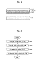
- FIG. 2 shows a structure of a heat transfer film according to one embodiment of the present invention
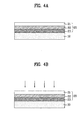
- FIG. 3 is a block diagram schematically showing a method of manufacturing partition walls according to the embodiment of the present invention.
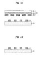
- FIGs. 4A to 4D show a process for manufacturing partition walls according to another embodiment of the present invention.
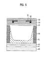
- FIG. 5 shows a cross-sectional view of a plasma display panel manufactured using a method of manufacturing a plasma display panel according to yet another embodiment of the present invention.
- FIG. 2 shows a structure of a heat transfer film 20 according to one embodiment of the present invention.
- the heat transfer film 20 may include a base film 21, a light-heat transforming layer 22 formed on the base film 21, and a partition wall material layer 23 formed on the light-heat transforming layer 22.
- the heat transfer film 20 may further include a transmission layer between the light-heat transforming layer 22 and the partition wall material layer 23.
- FIG. 2 shows arrangement of the heat transfer film 20 including the partition wall material layer 23, the light-heat transforming layer 22 and the base film 21 before the heat transfer film 20 is disposed on a substrate 10.
- the partition wall material layer 23 of the heat transfer film 20 faces the substrate 10 to be attached to the surface of the substrate 10.
- the heat transfer film 20 a portion where partition walls are formed is illuminated with light from a light source such as a laser.
- the illuminated light is transformed into heat through the light-heat transforming layer 22, whereby the partition wall material layer 23 is selectively transferred on the substrate 10.
- the light-heat transforming layer 22 may absorb light from an energy source such as the laser, a xenon (Xe) lamp and a flash lamp. It is preferable to use the laser capable of achieving the most excellent transfer performance.
- the laser may be a common laser such as a solid laser, a gas laser, a semiconductor laser, and a dye laser.
- the base film 21 is formed of, preferably, a transparent polymer, but the material of the base film 21 is not limited thereto.
- the polymer may include polyethylene, polyester terephthalate, polyacryl, polyepoxy, polyethylene, polystyrene and the like. Generally, a polyethylene terephthalate film is used for the base film 21.
- the base film 21 is a thickness of about 10 ⁇ 500 ⁇ m.
- the base film 21 serves as a support film.
- the light-heat transforming layer 22 is made of a light absorptive material capable of absorbing light, which is one selected from a group consisting of an organic film including a laser light absorptive material, metal and a combination thereof.
- the film having the properties includes metal, oxide and sulfide of the metal, an organic film made of a polymer containing carbon black, graphite or infrared dye.
- the metal and oxide and sulfide of the metal may include metal such as aluminum (Al), silver (Ag), chrome (Cr), tin (Sn), nickel (Ni), titanium (Ti), cobalt (Co), zinc (Zn), gold (Au), copper (Cu), tungsten (W), molybdenum (Mo), lead (Pb), oxide thereof, and a mixture thereof. It is preferable to use aluminum (Al), silver (Ag) and oxide thereof.
- the organic film made of a polymer containing carbon black, graphite or infrared dye may include only (meta)acrylate oligomer such as acryl (meta)acrylate oligomer, ester (meta)acrylate oligomer, epoxy (meta)acrylate oligomer and urethane (meta)acrylate oligomer, which is an organic substance in which a coloring agent or a dispersing agent such as paint and dye is dispersed in polymer-containing resin.
- the organic film may include a mixture of oligomer and (meta)acrylate monomer or only (meta)acrylate monomer. It is preferable to use carbon black or graphite having a particle diameter of 0.5 ⁇ m or less and an optical density of 0.1 ⁇ 4.
- the light-heat transforming layer 22 may include a material for improving transfer performance to efficiently transfer the partition wall material layer 23. That is, the light-heat transforming layer 22 may include a material for providing a pressure required to transfer the partition wall material layer 23 of a light-exposed region.
- the light-heat transforming layer 22 may include a polymer having a relatively low decomposition temperature (about 350 °Cor less, generally, about 325 °C or less, more generally, about 280 °Cor less), but it is not limited thereto. In case of a polymer having one or more decomposition temperature, the first decomposition temperature should be 350 °Cor less.
- the light-heat transforming layer 22 may be formed to have a single-layer or multi-layer structure.
- a polymer used for the transmission layer may include (a) polycarbonate having a low decomposition temperature (Td) such as polypropylene carbonate; (b) a substituted styrene polymer having a low decomposition temperature such as poly(alpha-methylstyrene); (c) polyacrylate and polymethacrylate ester such as polymethylmethacrylate and polybutylmethacrylate; (d) a cellulose substance having a low decomposition temperature (Td) such as cellulose acetate butyrate and nitrocellulose; and (e) other polymers such as polyvinyl chloride, poly(chlorovinyl chloride) polyacetal, polyvinylidene chloride, polyurethane having a low decomposition temperature (Td), polyester, polyorthoester, acrylonitrile, a substituted acrylonitrile polymer, maleic acid resin and a copolymer thereof.
- the transmission layer may include a polymer mixture.
- the transmission layer may include a material which emits nitrogen gas, hydrogen gas or the like due to decomposition reaction occurring when it absorbs light or heat, for example, pentaerythritol tetranitrate (PETN) and trinitrotoluene (TNT).
- PETN pentaerythritol tetranitrate
- TNT trinitrotoluene
- the partition wall material layer 23 may include a pasted material containing a partition wall material, but it is not limited thereto. Further, the partition wall material layer 23 may be coated as photosensitive paste, a sheet or slurry. The partition wall material layer 23 includes glass powder having a softening point ranging from 300 to 600 °C.
- the glass powder may be one selected from a group consisting of a mixture of lead oxide (PbO), boron oxide (B 2 O 3 ) and silicon oxide (SiO 2 ), a mixture of zinc oxide (ZnO), boron oxide (B 2 O 3 ) and silicon oxide (SiO 2 ), a mixture of lead oxide (PbO), boron oxide (B 2 O 3 ), silicon oxide (SiO 2 ) and aluminum oxide (Al 2 O 3 ), and a mixture of lead oxide (PbO), zinc oxide (ZnO), boron oxide (B 2 O 3 ) and silicon oxide (SiO 2 ).
- the partition wall material layer 23 may include a binder.
- the binder may be made of a polymer having a decomposition temperature of about 250 °C or more, particularly, about 350 °C or more.
- a photoresist may be used as the binder.
- the binder forms a film capable of being coated with solution or dispersion solution.
- a commonly-used binder has a melting point of about 250 °C or less, and is plasticized at a glass transition temperature of about 70 °C or less.
- a binder capable of being easily liquefied or heat-melted, for example, low-melting wax efficiently serves as a cobinder to lower a melting point of a texture layer. However, if the binder has fluidity or low durability, it should be avoided to use it alone.
- a polymer of the binder is not self-oxidized, decomposed or deteriorated at the temperature reached when it is exposed to a laser.
- an exposed region of the texture layer including the texture material and the binder is transferred without being damaged, thereby obtaining improved durability.
- the binder may include a copolymer of styrene and (meth)acrylate ester such as styrene/methylmethacrylate; a copolymer of styrene and an olefin monomer such as styrene/ethylene/butylenes; a copolymer of styrene and acrylonitrile; a fluoropolymer; a copolymer of (meth)acrylate ester, ethylene and carbon monoxide; polycarbonate having a proper decomposition temperature; a (meth)acrylate polymer and a copolymer of (meth)acrylate; polysulfone; polyurethane; and polyester.
- a monomer for the polymer may be substituted or unsubstituted.
- a substituent may include halogen, oxygen and nitrogen containing a substituent.
- a polymer mixture may be used as the substituent.
- a transmission layer may be further disposed between the light-heat transforming layer 22 and the partition wall material layer 23.
- the transmission layer may include a material for improving transfer performance to efficiently transfer the partition wall material layer 23. That is, the transmission layer may include a material for providing a pressure required to transfer the partition wall material layer of a light-exposed region.
- the transmission layer may include a polymer having a relatively low decomposition temperature (about 350 °C or less, generally, about 325 °C or less, more generally, about 280 °C or less), but it is not limited thereto. In case of a polymer having one or more decomposition temperature, the first decomposition temperature should be about 350 °C or less.
- a polymer used for the transmission layer may include (a) polycarbonate having a low decomposition temperature (Td) such as polypropylene carbonate; (b) a substituted styrene polymer having a low decomposition temperature such as poly(alpha-methylstyrene); (c) polyacrylate and polymethacrylate ester such as polymethylmethacrylate and polybutylmethacrylate; (d) a cellulose substance having a low decomposition temperature (Td) such as cellulose acetate butyrate and nitrocellulose; and (e) other polymers such as polyvinyl chloride, poly(chlorovinyl chloride) polyacetal, polyvinylidene chloride, polyurethane having a low decomposition temperature (Td), polyester, polyorthoester, acrylonitrile, substituted acrylonitrile polymer, maleic acid resin and a copolymer thereof.
- the transmission layer may include a polymer mixture.
- the transmission layer may include a material which emits nitrogen gas, hydrogen gas or the like due to decomposition reaction occurring when it absorbs light or heat, for example, pentaerythritol tetranitrate (PETN) and trinitrotoluene (TNT).
- PETN pentaerythritol tetranitrate
- TNT trinitrotoluene
- a method of manufacturing partition walls of a plasma display panel using the heat transfer film according to the present invention includes the steps of forming the heat transfer film 20 including a base film, a light-heat transforming layer and a partition wall material layer on the substrate 10; illuminating light on the heat transfer film 20; and separating the heat transfer film 20 from the substrate 10 to form a pattern of partition walls 11 on the substrate 10.
- FIG. 3 is a block diagram schematically showing the method of manufacturing partition walls of a plasma display panel according to the embodiment of the present invention.
- a dielectric layer is formed on a lower substrate (S510).
- the above-described heat transfer film is coated on the dielectric layer (S520).
- laser light is illuminated on the heat transfer film such that the heat transfer film is patterned into a partition wall pattern (S530).
- the heat transfer film is separated from the lower substrate to form partition walls on the dielectric layer in accordance with the partition wall pattern (S540).
- FIGs. 4A to 4D show a process for manufacturing the partition walls 11 using the above-described heat transfer film 20 according to another embodiment of the present invention.
- the above-described heat transfer film 20 is deposited on the substrate 10. Since the heat transfer film is described in detail before, the description thereof is omitted.
- the substrate 10 may be a glass substrate, a plastic substrate, or a transparent electrode.
- light is illuminated on the heat transfer film 20 in accordance with a partition wall pattern to be formed.
- light may be illuminated on the heat transfer film or on the substrate.
- An energy source used in this embodiment may be a laser, a xenon (Xe) lamp, a flash lamp or the like. It is preferable to use the laser capable of achieving the most excellent transfer performance.
- the laser may be a common laser such as a solid laser, a gas laser, a semiconductor laser, and a dye laser. Further, laser beam may have a circular shape or other shapes.
- laser light has a wavelength of about 300 ⁇ 450 nm.
- the light activates the light-heat transforming layer 22 through a transfer device, thereby emitting heat by heat decomposition reaction.
- the emitted heat causes decomposition reaction in the light-heat transforming layer or the transmission layer.
- the partition wall material layer 23 is separated from the heat transfer film 20 and partition walls are transferred on the substrate 10 in a desired pattern.
- the heat transfer film 20 is separated from the substrate 10. Since a region on which light is not illuminated is attached on the heat transfer film 20, the region is also removed by separating the heat transfer film 20 from the substrate 10. Accordingly, the partition walls 11 are formed on the region on which light is selectively illuminated and transfer is performed.
- the above-described method of manufacturing partition walls may be used in any case of manufacturing patterned partition walls independent of application fields. Particularly, the above-described method may be applied to a method of manufacturing electrodes of a plasma display panel.
- FIG. 5 shows a cross-sectional view of a plasma display panel manufactured using a method of manufacturing a plasma display panel according to yet another embodiment of the present invention.
- the plasma display panel includes a front plate having a pair of sustain electrodes 31 formed to be spaced into a specified pattern in a bottom portion of a front substrate 30, a front dielectric layer 33 formed to cover the sustain electrodes 31 and a protective film layer 34 formed on the bottom of the front dielectric layer 33; a rear plate having address electrode 41 formed on a rear substrate 40 to be perpendicular to a pair of the sustain electrodes 31; and partition walls 50 formed on the rear plate to define a discharge space.
- a pair of bus electrodes 32 shown in FIG. 5 may be omitted.
- a phosphor layer 51 may be coated on the partition walls and the rear plate.
- the plasma display panel further includes a rear dielectric layer 42.
- the structure of the plasma display panel according to the present invention is not limited to the structure shown in the drawing. Modification, addition, and omission may be made using any technique known in the art.
- a pair of the sustain electrodes 31, a pair of the bus electrodes 32, or the address electrode 41 may be manufactured using the above-described heat transfer film 20. Further, it is possible to improve the method of manufacturing electrodes using the heat transfer film 20.
- the protective film layer 34 is formed on the front dielectric layer 33 to complete the front plate of the plasma display panel.
- the protective film layer prevents the front dielectric layer from being damaged by sputtering, thereby increasing secondary electron emission efficiency as well as prolonging the life of PDP.
- the material of the protective film layer may include magnesium oxide (MgO), zirconium oxide (ZrO), hafnium oxide (HfO), cesium oxide (CeO 2 ), thorium oxide (ThO 2 ), lanthanium oxide (La 2 O 3 ), or the like. It is most preferable to use magnesium oxide (MgO) having a high secondary electron emission coefficient and excellent plasma resistance.
- the magnesium oxide (MgO) may be formed using a vacuum deposition method such an electron beam deposition method.
- the rear plate is manufactured separately from the above-described front plate.
- the address electrode 41 is formed on the rear substrate 40 to be perpendicular to a pair of the sustain electrodes.
- the rear dielectric layer 42 is formed to cover the address electrode (or omitted).
- the partition walls 50 are formed on the rear dielectric layer.
- the material and structure of the partition walls 50 may vary using any technique known in the art.
- the partition walls may be stripe-type partition walls, closed-type partition walls or delta-type partition walls.
- the partition walls are formed using the heat transfer film 20 according to one embodiment of the present invention.
- the phosphor layer 51 is coated on the rear dielectric layer and the partition walls 50, and they are attached to the front plate, thereby completing the plasma display panel.
- the partition walls 50 are formed using the heat transfer film by laser patterning in a transfer process.
- the partition walls 50 it is possible to form the partition walls having a fine pitch without using a photomask by simplifying the process and reducing material and process costs.
- graded partition walls having different heights in horizontal and vertical directions may be formed by controlling the wavelength of illuminated laser light in a transfer process of the above-described method.
- the illuminated laser light has a wavelength in a range of about 360 ⁇ 370 nm or about 400 ⁇ 410 nm, most preferably, a wavelength of about 365 nm or about 405 nm.
- the partition walls can be formed through a simple process using laser light or the like without using a mask. Accordingly, it is possible to simplify the process and reduce the mask cost compared to a conventional partition wall manufacturing method having a problem such as high process cost.
- the method according to the present invention is appropriate for scaling-up and mass production. Further, since the developing process is not necessary, a partition wall material can be saved, thereby providing effects such as cost reduction.
- partition walls having a fine pitch through a simple process, thereby increasing stability of the partition walls.
Landscapes
- Physics & Mathematics (AREA)
- Engineering & Computer Science (AREA)
- Optics & Photonics (AREA)
- Manufacturing & Machinery (AREA)
- Electromagnetism (AREA)
- Plasma & Fusion (AREA)
- Gas-Filled Discharge Tubes (AREA)
- Thermal Transfer Or Thermal Recording In General (AREA)
- Laminated Bodies (AREA)
Applications Claiming Priority (1)
| Application Number | Priority Date | Filing Date | Title |
|---|---|---|---|
| KR1020060061954A KR20080003554A (ko) | 2006-07-03 | 2006-07-03 | 열전사 필름, 이를 이용하는 격벽 제조 방법 및 플라즈마디스플레이 패널의 제조 방법 |
Publications (1)
| Publication Number | Publication Date |
|---|---|
| EP1876027A1 true EP1876027A1 (de) | 2008-01-09 |
Family
ID=38515860
Family Applications (1)
| Application Number | Title | Priority Date | Filing Date |
|---|---|---|---|
| EP07111292A Withdrawn EP1876027A1 (de) | 2006-07-03 | 2007-06-28 | Wärmeübertragungsfolie und Verfahren zur Herstellung von Trennwänden für eine Plasmaanzeigetafel damit |
Country Status (4)
| Country | Link |
|---|---|
| US (1) | US20080124659A1 (de) |
| EP (1) | EP1876027A1 (de) |
| JP (1) | JP2008016448A (de) |
| KR (1) | KR20080003554A (de) |
Cited By (1)
| Publication number | Priority date | Publication date | Assignee | Title |
|---|---|---|---|---|
| CN113793551A (zh) * | 2021-09-14 | 2021-12-14 | 山东泰宝信息科技集团有限公司 | 全息激光镭射信息低温烤花产品及其制备方法 |
Families Citing this family (3)
| Publication number | Priority date | Publication date | Assignee | Title |
|---|---|---|---|---|
| JP5864926B2 (ja) * | 2011-07-14 | 2016-02-17 | 東京応化工業株式会社 | 積層体、分離方法、及び製造方法 |
| JP2014079930A (ja) * | 2012-10-15 | 2014-05-08 | Nippon Carbide Ind Co Inc | レーザー転写マーキング用フィルムおよびそれを用いたレーザーマーキング品 |
| KR102620974B1 (ko) | 2018-10-05 | 2024-01-05 | 삼성전자주식회사 | 디스플레이 장치 및 그 제조 방법 |
Citations (7)
| Publication number | Priority date | Publication date | Assignee | Title |
|---|---|---|---|---|
| US4670307A (en) * | 1985-05-28 | 1987-06-02 | Matsushita Electric Industrial Co., Ltd. | Thermal transfer recording sheet and method for recording |
| EP0836892A2 (de) * | 1996-10-21 | 1998-04-22 | Dai Nippon Printing Co., Ltd. | Übertragungsschicht und Verfahren zur Herstellung eines Musters |
| US20010008825A1 (en) * | 1996-08-11 | 2001-07-19 | Osamu Toyoda | Method of manufacturing panel assembly used to assemble display panel and transfer material sheet |
| EP1226974A1 (de) * | 1999-10-29 | 2002-07-31 | 3M Innovative Properties Company | Donorblatt, farbfilter und organische el-vorrichtung, und herstellungsverfahren dafür |
| US20050206034A1 (en) * | 2004-01-06 | 2005-09-22 | Chikafumi Yokoyama | Transfer mold, production method thereof and production method of fine structure |
| US20050253884A1 (en) * | 2004-05-11 | 2005-11-17 | Ryoichi Matsumoto | Droplet ejecting apparatus, electro-optic device, electronic apparatus, and droplet ejecting method |
| US20060051604A1 (en) * | 2002-03-23 | 2006-03-09 | Arne Koops | Multilayer laser transfer film for permanently inscribing parts |
-
2006
- 2006-07-03 KR KR1020060061954A patent/KR20080003554A/ko not_active Abandoned
-
2007
- 2007-06-28 EP EP07111292A patent/EP1876027A1/de not_active Withdrawn
- 2007-06-29 JP JP2007171775A patent/JP2008016448A/ja not_active Withdrawn
- 2007-07-02 US US11/772,678 patent/US20080124659A1/en not_active Abandoned
Patent Citations (7)
| Publication number | Priority date | Publication date | Assignee | Title |
|---|---|---|---|---|
| US4670307A (en) * | 1985-05-28 | 1987-06-02 | Matsushita Electric Industrial Co., Ltd. | Thermal transfer recording sheet and method for recording |
| US20010008825A1 (en) * | 1996-08-11 | 2001-07-19 | Osamu Toyoda | Method of manufacturing panel assembly used to assemble display panel and transfer material sheet |
| EP0836892A2 (de) * | 1996-10-21 | 1998-04-22 | Dai Nippon Printing Co., Ltd. | Übertragungsschicht und Verfahren zur Herstellung eines Musters |
| EP1226974A1 (de) * | 1999-10-29 | 2002-07-31 | 3M Innovative Properties Company | Donorblatt, farbfilter und organische el-vorrichtung, und herstellungsverfahren dafür |
| US20060051604A1 (en) * | 2002-03-23 | 2006-03-09 | Arne Koops | Multilayer laser transfer film for permanently inscribing parts |
| US20050206034A1 (en) * | 2004-01-06 | 2005-09-22 | Chikafumi Yokoyama | Transfer mold, production method thereof and production method of fine structure |
| US20050253884A1 (en) * | 2004-05-11 | 2005-11-17 | Ryoichi Matsumoto | Droplet ejecting apparatus, electro-optic device, electronic apparatus, and droplet ejecting method |
Cited By (2)
| Publication number | Priority date | Publication date | Assignee | Title |
|---|---|---|---|---|
| CN113793551A (zh) * | 2021-09-14 | 2021-12-14 | 山东泰宝信息科技集团有限公司 | 全息激光镭射信息低温烤花产品及其制备方法 |
| CN113793551B (zh) * | 2021-09-14 | 2023-01-20 | 山东泰宝信息科技集团有限公司 | 全息激光镭射信息低温烤花产品及其制备方法 |
Also Published As
| Publication number | Publication date |
|---|---|
| KR20080003554A (ko) | 2008-01-08 |
| US20080124659A1 (en) | 2008-05-29 |
| JP2008016448A (ja) | 2008-01-24 |
Similar Documents
| Publication | Publication Date | Title |
|---|---|---|
| US6156433A (en) | Electrode for plasma display panel and process for producing the same | |
| EP1826804A1 (de) | Anzeigefilter und Anzeigevorrichtung damit | |
| US7612489B2 (en) | Display filter, display device including the display filter, and method of manufacturing the display filter | |
| US20080124659A1 (en) | Heat transfer film and method of manufacturing partition walls of plasma display panel using the same | |
| JP2006196455A (ja) | 感光性ペースト組成物、それを利用して製造されたpdp電極、及びそれを含むpdp | |
| US6508685B1 (en) | Plasma display panel and method of fabricating barrier rib therefor | |
| US20080038985A1 (en) | Dielectric sheet, plasma display panel using the same, and manufacturing method therefor | |
| US7857675B2 (en) | Plasma display panel and method for producing the same | |
| JPH09283018A (ja) | プラズマディスプレイパネルの製造方法およびプラズマディスプレイパネル | |
| EP1754722B1 (de) | Schwarzes, pastenförmiges Verbundmaterial, obere Platte einer Plasmaanzeigetafel und Herstellungsverfahren unter Verwendung desselben | |
| KR20070045658A (ko) | 전극 전사필름, 이를 이용한 전극 제조방법 및 플라즈마디스플레이 패널의 제조방법 | |
| US20090021169A1 (en) | Barrier ribs to reduce reflection of external light and plasma display panel (PDP) including such barrier ribs | |
| US7471042B2 (en) | Plasma display panel with an improved electrode | |
| KR20070071800A (ko) | 유전체 전사필름 및 이를 이용한 플라즈마 디스플레이패널의 제조방법 | |
| KR100380555B1 (ko) | 흑색층 형성용 흑색 페이스트 조성물 | |
| US20060125400A1 (en) | Green sheet, plasma display panel and method for manufacturing plasma display panel | |
| US7696692B2 (en) | Plasma display panel having an electrode structure including blackened dielectric layer and method of fabricating same | |
| KR101052738B1 (ko) | 디스플레이 장치용 광학 부재, 이를 제조하는 방법과 이를포함하는 디스플레이 장치용 필터 및 디스플레이 장치 | |
| JPH1190826A (ja) | プラズマディスプレイパネルの障壁形成用シート組成物及びガラスペースト組成物 | |
| JP4240940B2 (ja) | プラズマディスプレイパネルの製造方法 | |
| JPH10294058A (ja) | プラズマディスプレイ用平面基板の製造方法とその製造方法により製造したプラズマディスプレイ用平面基板 | |
| US20080246399A1 (en) | Multi-layer electrode, method of forming the same and plasma display panel comprising the same | |
| JP2001143625A (ja) | プラズマディスプレイパネル及びその製造方法 | |
| JP2009070807A (ja) | プラズマディスプレイパネル | |
| KR20050096996A (ko) | 플라즈마 디스플레이 패널 및 그의 제조방법 |
Legal Events
| Date | Code | Title | Description |
|---|---|---|---|
| PUAI | Public reference made under article 153(3) epc to a published international application that has entered the european phase |
Free format text: ORIGINAL CODE: 0009012 |
|
| 17P | Request for examination filed |
Effective date: 20070628 |
|
| AK | Designated contracting states |
Kind code of ref document: A1 Designated state(s): AT BE BG CH CY CZ DE DK EE ES FI FR GB GR HU IE IS IT LI LT LU LV MC MT NL PL PT RO SE SI SK TR |
|
| AX | Request for extension of the european patent |
Extension state: AL BA HR MK YU |
|
| AKX | Designation fees paid |
Designated state(s): DE FR GB NL |
|
| STAA | Information on the status of an ep patent application or granted ep patent |
Free format text: STATUS: THE APPLICATION HAS BEEN WITHDRAWN |
|
| 18W | Application withdrawn |
Effective date: 20090718 |