EP1876546B1 - Dispositif d'analyse de brouillage de cablage de circuit, programme d'analyse de brouillage, base de donnees utilisee dans le dispositif d'analyse de brouillage, et modele de ligne connecte asymetriquement - Google Patents
Dispositif d'analyse de brouillage de cablage de circuit, programme d'analyse de brouillage, base de donnees utilisee dans le dispositif d'analyse de brouillage, et modele de ligne connecte asymetriquement Download PDFInfo
- Publication number
- EP1876546B1 EP1876546B1 EP06731905.3A EP06731905A EP1876546B1 EP 1876546 B1 EP1876546 B1 EP 1876546B1 EP 06731905 A EP06731905 A EP 06731905A EP 1876546 B1 EP1876546 B1 EP 1876546B1
- Authority
- EP
- European Patent Office
- Prior art keywords
- line
- coupled line
- coupled
- interference
- asp
- Prior art date
- Legal status (The legal status is an assumption and is not a legal conclusion. Google has not performed a legal analysis and makes no representation as to the accuracy of the status listed.)
- Ceased
Links
Images











Classifications
-
- G—PHYSICS
- G06—COMPUTING OR CALCULATING; COUNTING
- G06F—ELECTRIC DIGITAL DATA PROCESSING
- G06F30/00—Computer-aided design [CAD]
- G06F30/30—Circuit design
- G06F30/36—Circuit design at the analogue level
- G06F30/367—Design verification, e.g. using simulation, simulation program with integrated circuit emphasis [SPICE], direct methods or relaxation methods
-
- H—ELECTRICITY
- H05—ELECTRIC TECHNIQUES NOT OTHERWISE PROVIDED FOR
- H05K—PRINTED CIRCUITS; CASINGS OR CONSTRUCTIONAL DETAILS OF ELECTRIC APPARATUS; MANUFACTURE OF ASSEMBLAGES OF ELECTRICAL COMPONENTS
- H05K1/00—Printed circuits
- H05K1/02—Details
- H05K1/0213—Electrical arrangements not otherwise provided for
- H05K1/0216—Reduction of cross-talk, noise or electromagnetic interference
-
- H—ELECTRICITY
- H05—ELECTRIC TECHNIQUES NOT OTHERWISE PROVIDED FOR
- H05K—PRINTED CIRCUITS; CASINGS OR CONSTRUCTIONAL DETAILS OF ELECTRIC APPARATUS; MANUFACTURE OF ASSEMBLAGES OF ELECTRICAL COMPONENTS
- H05K3/00—Apparatus or processes for manufacturing printed circuits
- H05K3/0005—Apparatus or processes for manufacturing printed circuits for designing circuits by computer
Definitions
- the present invention relates to an interference analysis device for analyzing the interference between wires provided on a circuit board, an interference analysis program, a database used in an interference analysis device, and an asymmetric coupled line model.
- a printed board (wiring board) mostly is designed with a CAD (Computer Aided Design) for printed board design using a computer (see, for example, Patent Document 1).
- CAD Computer Aided Design
- the interference between wires has a large influence on transmission characteristics.
- complicated wiring design including an asymmetric coupled line it is difficult to obtain the interference amount between wires by calculation, and there are a number of cases where the interference amount actually cannot be calculated. Therefore, the interference amount between wires mostly is considered by so-called guesswork by a skilled designer, instead of an electromagnetic analysis.
- the fact is that a printed board is developed by trial and error without considering the interference amount between wires.
- FIG. 24(a) is a diagram showing an example of a wiring pattern in one of inner layers included in a multi-layered board.
- wires to be analyzed have, for example, a wiring pattern 1000 (i.e., a complicated wiring pattern to be used actually) shown in FIG. 24(a)
- the wiring pattern 1000 cannot be subjected to an electromagnetic analysis as it is.
- the overall wiring pattern 1000 is divided into a mesh shape as in a wiring pattern 2000 shown in FIG. 24(b) .
- An analysis model in each divided cell is subjected to an electromagnetic analysis.
- the interaction between the respective cells is calculated, whereby the overall electromagnetic analysis is completed.
- the interference amount between wires is obtained from the results of the overall electromagnetic analysis.
- a printed board to be analyzed is a multi-layered board of 8 layers, having a size of 40 mm ⁇ 40 mm, the number of nets (the number of wires connecting components) included in the printed board is 550, and the number of vias electrically connecting layers is 5000, the following results are predicted.
- a configuration-oriented SPICE model for multiple couple lines in an inhomogeneous medium is presented in A. Tripathi et al.: "A configuration-oriented SPICE model for multiconductor transmission lines in an inhomogeneous medium", IEEE Transactions on microwave theory and techniques, IEEE Service Center, Piscataway, NJ, US, vol., 46, no. 12, 1 December 1998 .
- the circuit model consists of a network of uncoupled transmission lines and is readily modeled with simulation tools like LIBRA and SPICE, and provides an equivalent-circuit representation which is simple and topologically meaningful as compared to the model based on modal decomposition.
- This configuration-oriented model is derived by decomposing the immittance matrices associated with an n coupled-line 2n-port system.
- Time- and frequency-domain simulations of typical coupled-line multiports are included to exemplify the utility of the model.
- the model is useful for the simulation and design of general single and multilayer coupled-line components such as filters and couplers and investigation of signal integrity issues, including crosstalk in interconnects associated with high-speed digital- and mixed-signal electronic modules and packages.
- the object of the present invention is to provide an interference analysis device capable of shortening a processing time significantly while maintaining high precision.
- an interference analysis device capable of shortening a processing time significantly while maintaining high precision can be realized.
- An interference analysis device which analyzes interference between wires provided on a circuit board and including a coupled line, includes: an input unit that inputs design data representing an arrangement of the wires on the circuit board; a selection unit that selects, as an analysis region, at least a part of the circuit board represented by the design data; a division unit that divides the wires in the analysis region into segments to be units for calculating a circuit matrix; a calculation unit that calculates a circuit matrix with respect to a coupled line constituted by two segments adjacent to each other among the segments divided by the division unit, or a single segment; and an analysis unit that obtains a degree of electromagnetic interference between the wires in the analysis region based on the circuit matrix, wherein the calculation unit calculates the circuit matrix of the coupled line, using a parameter set obtained by adding an asymmetry parameter representing asymmetry of the coupled line to RLGC parameters containing a resistance (R), an inductance (L), a parallel conductance (G), and a capacitance (C) of a transmission line
- the calculation unit calculates a circuit matrix of the coupled line, using a parameter set obtained by adding an asymmetry parameter representing asymmetry of the coupled line to RLGC parameters containing a resistance (R), an inductance (L), a parallel conductance (G), and a capacitance (C) of a transmission line in the coupled line, so that even an asymmetric coupled line can be processed in a similar manner to that of a symmetric coupled line. Therefore, a circuit matrix can be obtained within a short processing time.
- the analysis unit obtains a degree of electromagnetic interference between wires based on the circuit matrix, so that a processing time can be shortened substantially while high precision is maintained.
- the wires adjacent to each other are not limited to parallel wires.
- the asymmetry parameter interpolates asymmetry of an asymmetric coupled line to enable the asymmetric coupled line to be dealt with as a symmetric coupled line.
- the calculation unit obtains a circuit matrix, using the asymmetric parameter, so that a processing time for obtaining a circuit matrix can be shortened substantially.
- the asymmetry parameter is used for rotating the circuit matrix mathematically so that an odd mode and an even mode have a symmetric relationship of 1:1 in an asymmetric coupled line.
- the asymmetry parameter is used for rotating the circuit matrix mathematically so that an odd mode and an even mode have a symmetric relationship of 1:1 in an asymmetric coupled line. Therefore, the calculation unit can deal with an asymmetric coupled line in a similar manner to that of a symmetric coupled line by using the asymmetry parameter.
- the asymmetry parameter may be calculated using an impedance in a case where a line included in the coupled line is present alone. Consequently, an asymmetry parameter can be expressed approximately with each impedance of lines included in a coupled line.
- the case where the first line or the second line is present alone means the case where the first line and the second line are spaced away from each other sufficiently so as not to influence each other.
- asymmetry parameters P1, P2, and P3 in a coupled line constituted by a first line, a second line, and a third line and having a configuration in which a distance between the first line and the third line is larger than a distance between the other sets of two lines may be calculated by the following Expressions (1-a), (1-b), and (1-c), respectively, and the calculation unit may calculate a circuit matrix of the coupled line, using P1, P2, and P3 as asymmetry parameters:
- P 1 impedance in an even mode between the first line and the second line / impedance in an even mode between the third line and the second line 1 / 2
- P 2 impedance of the first line in a case where the second line is grounded / impedance of the third line in a case where the second line is grounded 1 / 2
- P 3 impedance in an odd mode between the first line and the second line / impedance in an odd mode between the third line and the second line 1 / 2
- the division unit divides two wires, that are present in the analysis region so as to be adjacent to each other, in such a manner that a position that is a boundary between a portion where the two wires are arranged in parallel and a portion where the two wires are not arranged in parallel is included in a boundary of the segments.
- the above-mentioned division unit divides wires so that the number of segments arranged in parallel to each other is larger. Therefore, a number of line segments constituted by segments arranged in parallel to each other are present. A circuit matrix of a coupled line constituted by segments arranged in parallel to each other is calculated with a small amount of processing. Consequently, the processing time in the calculation unit is shortened.
- the circuit matrix may be an S matrix.
- the interference analysis device further includes a recording unit storing a plurality of parameter sets obtained respectively by adding an asymmetry parameter representing asymmetry of the coupled line to RLGC parameters containing a resistance (R), an inductance (L), a parallel conductance (G), and a capacitance (C) of a transmission line in the coupled line, wherein, in the recording unit, the parameter sets are recorded so as to be associated with line information representing configurations of coupled lines regarding the parameter sets, and regarding a coupled line in the analysis region, the calculation unit searches the recording unit for line information matched with the configuration of the coupled line, and calculates a circuit matrix of the coupled line, using a parameter set corresponding to the line information obtained as a result of the search.
- a recording unit storing a plurality of parameter sets obtained respectively by adding an asymmetry parameter representing asymmetry of the coupled line to RLGC parameters containing a resistance (R), an inductance (L), a parallel conductance (G), and a capacitance (C) of a transmission line in the
- the calculation unit obtains the parameter set from the recording unit, so that it is not necessary to obtain a parameter set by calculation. Consequently, a processing time is shortened.
- the calculation unit performs interpolation using a parameter set of line information close to a configuration of the coupled line regarding the search, thereby obtaining a parameter set in the coupled line.
- the calculation unit can obtain a parameter set by interpolation. Therefore, the number of parameter sets to be recorded in the recording unit may be small. Consequently, the above-mentioned search can be conducted quickly.
- the calculation unit calculates a circuit matrix of the coupled line regarding a plurality of different frequencies, using a parameter set obtained by adding an asymmetry parameter representing asymmetry of the coupled line to RLGC parameters containing a resistance (R), an inductance (L), a parallel conductance (G), and a capacitance (C) of a transmission line in the coupled line.
- the calculation unit calculates a circuit matrix of the coupled line regarding a plurality of different frequencies, so that the analysis unit can obtain a degree of interference between wires at any frequency.
- the interference analysis device further includes: a condition setting unit that sets an interference analysis condition containing an interference amount reference value; a pair selection unit that selects a pair of wires to be analyzed among wires in the analysis region; an interference amount calculation unit that calculates an interference amount between the pair of wires based on a connection condition representing a connection relationship between segments included in the pair of wires and the circuit matrix calculated in the calculation unit; and a judgment unit that judges whether or not interference between the pair of wires causes a problem, comparing the interference amount reference value with the interference amount.
- the interference amount calculation unit calculates an interference amount between the pair of wires selected by the pair selection unit, so that the judgment unit can judge whether or not interference between the pair of wires causes a problem. Consequently, a pair of wires, that cause a problem, are extracted.
- Data according to the present invention allowing a computer to be used in processing of obtaining a circuit matrix of a coupled line having various configurations, contains a parameter set obtained by adding an asymmetry parameter representing asymmetry of the coupled line to RLGC parameters containing a resistance (R), an inductance (L), a parallel conductance (G), and a capacitance (C) of a transmission line in the coupled line, and line information representing a configuration of the coupled line, associated with the parameter set.
- RLGC parameters containing a resistance (R), an inductance (L), a parallel conductance (G), and a capacitance (C) of a transmission line in the coupled line, and line information representing a configuration of the coupled line, associated with the parameter set.
- a circuit matrix in a coupled line having a configuration represented by the line information can be obtained by a computer.
- the parameter set contains an asymmetry parameter representing the asymmetry of the coupled line. Therefore, even if the coupled line represented by the line information is an asymmetric coupled line, the computer can process the asymmetric coupled line in a similar manner to that of a symmetric coupled line.
- An asymmetric coupled line model causing a computer to be used in processing of calculating a circuit matrix in an asymmetric coupled line included in wires provided on a circuit, includes a parameter set obtained by adding an asymmetry parameter representing asymmetry of the coupled line to RLGC parameters containing a resistance (R), an inductance (L), a parallel conductance (G), and a capacitance (C) per unit length of a transmission line in the coupled line on the circuit, wherein circuit characteristics of the coupled line are represented as data readable by a computer, using the parameter set.
- the asymmetric coupled line calculates a circuit matrix in a coupled line using a parameter set including the asymmetric parameter, so that the circuit matrix in any coupled line can be calculated with a small amount of processing.
- An interference analysis program causes a computer to execute processing of analyzing interference between wires provided on a circuit board and including a coupled line, the program causing the computer to execute: input processing of inputting design data that represents an arrangement of wires in the circuit board; selection processing of selecting, as an analysis region, at least a part of the circuit board represented by the design data; division processing of dividing the wires in the analysis region into segments to be units for calculating a circuit matrix; calculation processing of calculating a circuit matrix, regarding a coupled line constituted by two segments adjacent to each other among the segments divided by the division processing, or a single segment; and analysis processing of obtaining a degree of electromagnetic interference between the wires in the analysis region based on the circuit matrix, wherein the calculation processing calculates a circuit matrix of the coupled line, using a parameter set obtained by adding an asymmetry parameter representing asymmetry of the coupled line to RLGC parameters containing a resistance (R), an inductance (L), a parallel conductance (G), and a capacitance (C) of
- the asymmetry parameter interpolates asymmetry of an asymmetric coupled line to enable the asymmetric coupled line to be dealt with as a symmetric coupled line.
- the asymmetry parameter is used for rotating the circuit matrix mathematically so that an odd mode and an even mode have a 1:1 symmetric relationship in the asymmetric coupled line.
- the asymmetry parameter P is calculated by the above Expression (1) in a coupled line constituted by a first line and a second line.
- the present embodiment relates to an interference analysis device that analyzes the interference between wires provided on a circuit board.
- FIG. 1 is a functional block diagram showing an exemplary configuration of an interference analysis device according to the present embodiment.
- an interference analysis device 10 includes a condition setting unit 1, an input unit 2, a selection unit 3, a pair selection unit 4, a division unit 5, a calculation unit 6, an analysis unit 7, and a recording unit 9.
- the analysis unit 7 includes an interference amount calculation unit 71 and a judgment unit 72.
- the recording unit 9 is provided with an RLGC parameter database 104.
- the RLGC parameter database 104 previously stores an RLGC parameter and an asymmetry parameter in any coupled line. The RLGC parameter and the asymmetry parameter will be described later.
- the interference analysis device 10 is connected to a CAD 8.
- the CAD 8 stores design data on a circuit board to be subjected to an interference analysis.
- the condition setting unit 1 sets conditions of an analysis performed by the interference analysis device 10. For example, the condition setting unit 1 receives an input of analysis conditions from a designer via an input device such as a keyboard or a mouse. The analysis conditions set in the condition setting unit 1 are stored in the recording unit 9.
- the input unit 2 reads the design data on the circuit board stored in the CAD 8, and sets the design data to be available in the interference analysis device 10.
- the selection unit 3 selects at least a part of the circuit board represented by the design data read by the input unit 2 as an analysis region.
- the pair selection unit 4 further selects a pair of wires from those included in the analysis region selected by the selection unit 3.
- the division unit 5 divides the pair of wires selected by the pair selection unit 4 into segments.
- the calculation unit 6 calculates a circuit matrix for each segment divided by the division unit 5.
- the design data input in the input unit 2, and various parameters stored in the RLGC parameter database are used for calculating a circuit matrix.
- the interference amount calculation unit 71 calculates an interference degree in the pair of wires based on the circuit matrix calculated for each segment.
- the judgment unit 72 judges whether or not the interference in the pair of wires causes a problem, based on the conditions set in the condition setting unit 1, and the calculation results in the interference amount calculation unit 71.
- FIG. 2 is a diagram showing an exemplary hardware configuration of the interference analysis device 10.
- the interference analysis device 10 is composed of a CPU (central processing unit) 101 performing an arithmetic operation, a ROM 102 storing a program and the like, a RAM 103 to be a working region or the like of the CPU, an external storage device 108 (e.g., a hard disk, a flash memory, a DVD, etc.) storing various set data and the like, an input device 105 (e.g., a keyboard, a mouse, etc.) receiving an input by an operator, a printing device 106 (e.g., a printer), and a display device 107 (a liquid crystal display, a CRT, etc.).
- a CPU central processing unit
- ROM 102 storing a program and the like
- RAM 103 to be a working region or the like of the CPU
- an external storage device 108 e.g., a hard disk, a flash memory, a DVD, etc.
- Each element is connected via a bus.
- the functions of the condition setting unit 1, the input unit 2, the selection unit 3, the pair selection unit 4, the division unit 5, the calculation unit 6, and the analysis unit 7 in FIG. 1 are realized when the CPU 101 executes a predetermined program stored, for example, in the ROM 102.
- the recording unit 9 the external storage device 108 can be used.
- the interference analysis device 10 also can be configured by incorporating a program for realizing the functions of the condition setting unit 1, the input unit 2, the selection unit 3, the pair selection unit 4, the division unit 5, the calculation unit 6, and the analysis unit 7 in a general computer.
- the program can be recorded on a computer-readable recording medium (e.g., an optical recording medium, a magnetic recording medium, a magnetooptical recording medium, a flash memory, etc.).
- the interference analysis device 10 also can be configured on the same computer as that of the CAD 8.
- the operation of the CAD 8 and that of the interference analysis device 10 can be executed by one device.
- the interference analysis device 10 executes a simulation of circuit wiring, so that the interference analysis device 10 also can be referred to as a circuit simulator in this sense.
- the hardware configuration of the interference analysis device 10 is not limited to the one shown in FIG. 2 .
- the function of the interference analysis device 10 may be distributed in a plurality of PCs or the like connected so as to communicate with each other through the Internet, LAN, or the like.
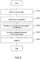
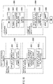
- FIG. 3 is a flowchart showing a basic flow of the interference analysis processing performed by the interference analysis device 10.
- the selection unit 3 selects at least a part of a region including an asymmetric coupled line as an analysis region (Step S10).
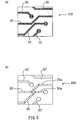
- FIG. 4(a) is a diagram showing an example of the analysis region selected by the selection unit 3.
- An analysis region 500 shown in FIG. 4(a) includes wires 201, 202, 203, and 204.
- FIG. 4(b) is a diagram showing an example of segment division.
- the wire 204 is divided into 8 segments including segments 30a, 30b.
- Each segment is a small region to be a unit for calculating a circuit matrix.
- a portion in which segments are adjacent to each other is set to be a coupled line.
- the coupled line refers to a pair of lines between which electromagnetic coupling is present to such a degree as not to be negligible.
- the segments 30a and 30e adjacent to each other in parallel are set to be a coupled line 35.
- not only lines provided on the same wiring layer, but also lines provided on different wiring layers are dealt with as coupled lines.
- segments constituting a coupled line are not necessarily parallel to each other. The detail of segment division will be described later.
- the calculation unit 6 calculates a circuit matrix (e.g., an S matrix) with respect to the segments divided in Step S20, or the coupled line constituted by the segments (Step S30).
- the calculation unit 6 obtains, for example, an S matrix of the coupled line 35.
- the S matrix of the coupled line 35 is an S matrix of four terminals. S matrices are obtained with respect to all the coupled lines in the analysis region 500.
- the S matrix (scattering matrix) defines characteristics of a circuit by the magnitude and phase of a wave related to the electric power that is input/output with respect to each terminal pair (port) of the circuit.
- Each element of the S matrix is called an S parameter.
- Step S30 the calculation unit 6 obtains an S matrix, using an RLGC parameter composed of a resistance (R), an inductance (L), a parallel conductance (G), and a capacitance (C) per unit length of a transmission line in the coupled line, with an asymmetry parameter (hereinafter, referred to as an ASP) added thereto. More specifically, the calculation unit 6 calculates S parameters using the RLGC parameter and the ASP.
- an asymmetry parameter hereinafter, referred to as an ASP
- the ASP is a parameter that interpolates the asymmetry of an asymmetric coupled line to enable the asymmetric coupled line to be dealt with as a symmetric coupled line.
- the calculation unit 6 can calculate S parameters of an asymmetric coupled line by using the ASP. Therefore, the interference analysis device 10 is suitable for analyzing a wiring pattern having an asymmetric coupled line to be used actually, rather than being used for analyzing a wiring pattern such as a test pattern composed of only a symmetric shape. The detail of the ASP will be described later.
- the interference amount calculation unit 71 calculates an interference amount between wires in the analysis region 500 based on the S matrix calculated by the calculation unit 6 (Step S40).
- the judgment unit 72 judges whether or not the interference between wires in the analysis region 500 causes a problem.
- the judgment unit 72 performs judgment, for example, by judging whether or not the interference amount calculated in Step S40 exceeds a previously set reference value.
- the circuit board to be analyzed is not divided into a mesh shape as a whole as in the conventional method shown in FIG. 24(b) , and only the wires are divided into segments as shown in FIG. 4(b) .
- a coupled line constituted by a pair of segments is represented by an S matrix. More specifically, the coupled line is replaced by an equivalent model. Interference (electromagnetic interference) is obtained based on the equivalent model.
- wires 30 are divided into a mesh shape, and an electric magnetic analysis is performed for each of a plurality of divided pieces. Therefore, a great amount of processing time is required.
- the wires 30 to be analyzed are extracted, and the wires 30 are divided into a plurality of segments including segments 30a. Therefore, a processing time is shortened substantially.
- the symmetric coupled line refers to a coupled line in which two lines constituting the coupled line have the same shape and the same electrical property, and the two lines and surrounding configurations are placed at positions symmetrical with respect to a symmetric surface.
- the surrounding configurations include, for example, the positional relationship between a line and a ground, the configuration and electrical property of a dielectric provided between the line and the ground, and the like.
- FIG. 6 is a diagram showing a configuration of the coupled line 800 in the case where the coupled line is symmetrical.
- the coupled line 800 is constituted by a first line 11 and a second line 12.
- the first line 11 and the second line 12 are placed on a substrate 15 in a symmetric configuration.
- a ground 32 is provided on a lower surface of the substrate 15.
- the first line 11 has ports P1 and P3, and the second line 12 has ports P2 and P4.
- the coupled line 800 has a symmetric configuration, so that some of the elements in the S matrix of the coupled line 800 can be expressed by the same S parameters.
- 4 kinds of S parameters: S11, S12, S13, and S14 are obtained, an S matrix can be obtained.
- 4 kinds of S parameters: S11, S12, S13, and S14 can be expressed by the following Expression 2.
- subscripts "e” and "o” respectively mean an even mode and an odd mode.
- S 11 ⁇ e + ⁇ o 2
- S 12 ⁇ e ⁇ ⁇ o 2
- S 13 ⁇ e + ⁇ o 2
- S 14 ⁇ e ⁇ ⁇ o 2
- Respective terms ⁇ e , ⁇ o , T e , T o in the above Expression 2 are represented by the following Expression 3.
- [Zsystem] is a normalized impedance (typically, 50 ⁇ ).
- Respective terms A e , B e , C e , D e and A o , B o , C o , D o in the above Expression 3 are represented by the following Expression 4.
- a e B e C e D e cosh ⁇ e l Z e sinh ⁇ e l 1 Z e sinh ⁇ e l cosh ⁇ e l
- a o B o C o D o cosh ⁇ o l Z o sinh ⁇ o l 1 Z o sinh ⁇ o l cosh ⁇ o l
- R is a resistance per unit length of a transmission line
- L is an inductance per unit length of a transmission line
- G is a parallel conductance per unit length of a transmission line
- C is a capacitance per unit length of a transmission line.
- the subscripts "e” and “o” respectively mean an even mode and an odd mode in the same way as in the above.
- ⁇ means an angular frequency of a transmission line
- ⁇ 2 ⁇ f(f: frequency).
- FIGS. 7(a) and (b) show the state of an electric field and a magnetic field in an even mode and an odd mode of the symmetric coupled line 800.
- the even mode and the odd mode are described in the following Reference Document.
- FIG. 7(a) shows the state of an electric field and a magnetic field in an even mode
- FIG. 7(b) shows the state of an electric field and a magnetic field in an odd mode.
- a resistance "R”, an inductance “L”, a parallel conductance “G”, a capacitance “C”, a frequency f, and a length "l” of a transmission line are required.
- the resistance "R”, the inductance “L”, the parallel conductance “G”, and the capacitance “C” are determined by the configuration of the coupled line 800.
- the configuration of the coupled line 800 includes, for example, at least one of a transmission line length in the first line 11 and the second line 12 constituting the coupled line 800, a wire width, a wire interval (Gap), the thickness of the substrate 15 that is a dielectric, a dielectric constant of the substrate 15, a dielectric loss, and the like.
- the configuration of such a coupled line is represented by, for example, design data on a circuit board input by the input unit 2.
- the interference analysis device 10 in the present embodiment obtains an S matrix of an asymmetric coupled line by an arithmetic operation using an arithmetic approach.
- the asymmetric coupled line is a coupled line that is not symmetrical.
- FIGS. 8 and 9 are diagrams showing an example of an asymmetric coupled line.
- a coupled line 900 shown in FIG. 8 the wire width of a first line 21 is different from that of a second line 22.
- FIG. 9 is a cross-sectional view of an asymmetric coupled line 950.
- the layer configuration of a first line 23 is different from that of a second line 24.
- the coupled line constituted by the two wires is an asymmetric coupled line.
- the characteristic impedance of each wire constituting a coupled line varies depending upon the difference in configuration of the coupled line, such as a wire width, a layer configuration, and a dielectric thickness. Therefore, the number of kinds of S parameters constituting an S matrix of an asymmetric coupled line is larger than that of a symmetric coupled line.
- an S matrix of a coupled line 900 shown in FIG. 8 will be shown in the following Expression 6.
- the calculation unit 6 can calculate 6 kinds of S parameters of an asymmetric coupled line from the RLGC parameters, using an ASP parameter.
- the inventors of the present application performed mathematical development of a complicated S matrix composed of 6 kinds of S parameters without proceeding toward the processing as shown in FIG. 24(b) , and used the ASP in the development, thereby having achieved a procedure just like the arithmetic operation of a symmetric coupled line.
- S parameters can be generated from the resistance in an even mode and an odd mode, the inductance, the parallel conductance, the capacitance (R e , L e , G e , C e , R o , L o , G o , C o ), the ASP, the transmission line length 1, and the frequency f. More specifically, S parameters cannot be obtained from R e , L e , G e , C e , R o , L o , G o , C o , the transmission line length 1, and the frequency f without the ASP, except for the case of a symmetric coupled line. Consequently, in order to obtain S parameters with respect to an asymmetric coupled line, as shown in FIG. 24(b) , it is necessary to perform an electromagnetic analysis with respect to a meshed model.
- the electric equivalent circuit of the coupled line 900 shown in FIG. 8 is represented by an equivalent circuit diagram of a 4-terminal circuit shown in FIG. 10 , and a circuit equation of the 4-terminal circuit represented by the equivalent circuit diagram shown in FIG. 10 is solved, whereby S parameters of the S matrix of the coupled line 900 can be calculated.
- F e denotes a 4-terminal circuit, and one terminal of the four terminals is connected to ports P1, P2 respectively via transformers TR1 e , TR2 e . Another terminal of the 4-terminal circuit F e is connected to ports P3, P4 respectively via transformers TR3 e , TR4 e . The remaining two terminals of the 4-terminal circuit F e are grounded.
- F o also is a 4-terminal circuit, and one terminal of the four terminals is connected to the ports P1, P2 respectively via transformers TR1 o , TR2 o . Another terminal of the 4-terminal circuit F o is connected to the ports P3, P4 respectively via the transformers TR3 o , TR4 o . The remaining two terminals of the 4-terminal circuit F o are grounded.
- the 4-terminal circuits F e , F o are equivalent circuits of one line.
- the circuit matrix of the 4-terminal circuit F e is represented by, for example, a matrix including A e , B e , C e , D e shown by the above Expression 4
- the circuit matrix of the 4-terminal circuit F o is represented by, for example, a matrix including A o , B o , C o , D o represented by the above Expression 4.
- the ratio between the winding number of a coil on the port P1 side in the transformer TR1 e and the winding number of a coil on the F e side is 1:RC 11 .
- the winding number ratios of the transformers TR2 e , TR1 o , TR2 o also are 1:RC 21 , 1:RC 12 , 1:RC 22 , respectively.
- the winding number ratio of the transformer TR1 e is the same as that of the transformer TR3 e .
- the winding number ratios are the same.
- Rc 11 , Rc 21 , Rc 12 , Rc 22 in each winding number ratio are values determined by the asymmetry of the coupled line 900. Theses values respectively are represented using the ASP, as shown in, for example, the following Expressions 7, 8, 9, and 10.
- Rc 11 1 + AS P 2 ASP
- Rc 21 1 + AS P 2 ASP
- the ASP in the above Expressions 7, 8, 9, and 10 is obtained approximately by, for example, the following Expression 11. Impedance of first line 21 alone Impedance of secont line 22 alone
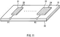
- the impedance of the first line 21 alone refers to the impedance of the first line 21 in the case where it is assumed that the first line 21 and the second line 22 are spaced away from each other sufficiently so as not to influence each other, as shown in FIG. 11 .
- the impedance of the second line 22 alone refers to the impedance of the second line 22 in the case where it is assumed that the first line 21 and the second line 22 are spaced away from each other sufficiently so as not to influence each other.
- the value that represents each difference degree of impedance of the lines included in a coupled line can be set to be an ASP representing asymmetry.
- the method for calculating an ASP is not limited to the calculation method using an impedance in the case where lines included in a coupled line are present alone.
- the asymmetric coupled line is replaced by an equivalent circuit with a configuration in which a circuit of a symmetric coupled line represented by RLGR parameters is connected to terminals via transformers represented by the ASP, and the circuit equation of the equivalent circuit is solved using the RLGC parameters and the ASP, whereby S parameters can be obtained.
- the data representing an equivalent circuit of a coupled line is represented by circuit data that represnets a circuit configuration, RLGC parameters (R e , L e , G e , C e ) in an even mode, RLGC parameters (R o , L o G o , C o ) in an odd mode, and an ASP.
- the RLGC parameters and the ASP are determined by the configuration of the coupled line.
- R e , L e , G e , C e , R o , L o , G o , C o , ASP, and circuit data can be recorded in, for example, the recording unit 9 as a coupled line model. Because of this, the calculation unit 6 can obtain an S matrix of a coupled line, using the coupled line model.
- the ASP is a parameter that interpolates asymmetry, thereby enabling the processing as if symmetry is kept. This is introduced originally by the inventors of the present application in order to obtain a wiring interference with good efficiency.
- An asymmetry parameter is a parameter for mathematically rotating an S matrix so that an odd mode and an even mode have a 1:1 symmetric relationship in an asymmetric coupled line.
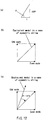
- FIGS. 12(a) to 12(c) are explanatory views schematically showing mathematical images of the ASP.
- an even mode and an odd mode have a 1:1 relationship. More specifically, in an equivalent model in the case of asymmetric wiring, an even mode and an odd mode are displaced from a 1:1 relationship.
- an S matrix composed of 4 rows and 4 columns of a coupled line is rotated mathematically by an angle ( ⁇ - ⁇ /4) so that an even mode and an odd mode have a 1:1 relationship (see FIG. 12(c) ).
- the processing is performed by introducing the ASP.
- the above Expressions 12 to 17 represent an example of the processing of rotating an S matrix so that an even mode and an odd mode have a 1:1 relationship.
- an S parameter of the S matrix represented by the above Expression 6 can be obtained by using 9 parameters composed of the RLGC parameter and the ASP in even/odd modes.
- the S parameters obtained by the above Expressions 12 to 17 are represented by a vector amount having a real part and an imaginary part.
- the absolute value of a coupling amount S21 between the ports P1 and P2 can be represented by the following Expression (2).
- S12 represents the coupling amount between the ports P1 and P2, which is the same value as that of S21.
- the absolute value and phase of a coupling amount S32 between the ports P2 and P3 can be represented by the following Expressions (6) and (7), respectively.
- S32 S23.
- S 32 real 2 + S 32 imag 2 1 / 2 tan ⁇ 32 S 32 imag / S 32 real
- the absolute value and phase of a coupling amount S43 between the ports P3 and P4 can be represented by the following Expressions (8) and (9), respectively.
- S43 S34.
- S 43 real 2 + S 43 imag 2 1 / 2 tan ⁇ 43 S 43 imag / S 43 real
- the absolute value and phase of a passing amount S31 between the ports P1 and P3 can be represented by the following Expressions (10) and (11), respectively.
- S31 S13.
- S 31 real 2 + S 31 imag 2 1 / 2 tan ⁇ 31 S 31 imag / S 31 real
- the absolute value and phase of a passing amount S42 between the ports P2 and P4 can be represented by the following Expressions (12) and (13), respectively.
- S42 S24.
- S 42 real 2 + S 42 imag 2 1 / 2 tan ⁇ 42 S 42 img / S 42 real
- the coupling amount is represented by, for example, S12, S21, S14, S41, S23, S32, S34, and S43 among S parameters in the coupled line 900 shown in FIG. 8 .
- the passing amount is reprsented by, for example, S13, S31, S24, and S42 among S parameters in the coupled line 900 shown in FIG. 8 .
- S parameters are calculated as complex numbers including a real part and an imaginary part, whereby the absolute value and phase of a coupling amount, and the absolute value and phase of a passing amount are calculated, as represented by the above Expressions (2) to (13). More specifically, in the coupled line 900 shown in FIG. 8 , the absolute value and phase of each coupling amount between the ports P1 and P2, between the ports P1 and P4, between the ports P3 and P2, and between the ports P3 and P4 are calculated, and in addition, the absolute value and phase of a passing amount between the ports P1 and P3 and between the ports P2 and P4 also are calculated.
- an exact interference amount cannot be calculated merely by considering the absolute value of a coupling amount in a coupled line dividied into segments.
- the phase of a coupling amount in a coupled line also is calculated simultaneously, and furthermore, both the absolute value and the phase of a passing amount can be calculated, the interference amount between wires can be calculated with higher precision.
- the smooth processing owing to the introduction of the ASP parameter is the result obtained by the study of the inventors of the present application.
- the achievement of the interference analysis device with the ASP introduced therein also is the result obtained by the inventors of the present application.
- the circuit matrix of a coupled line is not limited to an S matrix.
- a Z matrix, a Y matrix, an F matrix, and a T matrix can be used, in addition to the S matrix used often in the art.
- the Z, Y, F, T parameters (i.e., parameters constituing the Z matrix, the Y matrix, the F matrix, and the T matrix) and the S parameters (i.e., parameters constituting the S matrix) can be converted into each other. It is convenient to use the T parameters for synthesis with respect to the cascaded connection of a circuit. However, since there is a circuit that cannot be defined with the T parameters, the S parameters have higher general versatility.
- the interference analysis device 10 in the present embodiment can be used as a part of a design device of a circuit board for performing interference analysis processing.
- Embodiment 2 the processing in Embodiment 1 will be described in more detail.
- the configuration of the interference analysis device in Embodiment 2 is the same as that of the interference analysis device 10 shown in FIG. 1 .
- FIG. 13 is a flowchart showing the detail of the processings in Steps S20, S30, and S40 in the flowchart shown in FIG. 3 .
- Step S20 the division unit 5 performs a GND search (S531) and a segment division (S532).
- a ground pattern present in the analysis region i.e., a pattern in an earth or ground region is extracted.
- the division unit 5 when dividing wires into segments, can set a portion, in which the angle of a wire changes as in a boundary 31a shown in FIG. 4(b) , to be a boundary.
- a boundary dividing a wire into a portion 30c where two wires 204, 203 are arranged in parallel and a portion 30d where they are not arranged in parallel, as in a boundary 31b.
- the portion where two wires are not arranged in parallel for example, a portion crossing a wire in a different layer or a portion where the angle of a coupled line in the wire changes can be set to be a boundary of segments.
- the division unit 5 divides wires into segments so that the number of segment pairs parallel to each other is larger.
- the wires are divided into segments so that the number of parallel segments is larger, it becomes easier to shorten a processing time while maintaining high precision.
- the ground pattern extracted in the GND search (S531) also is considered.
- the division unit 5 can divide a wire so that a portion where the ground pattern is present in a layer and a portion where the ground pattern is not present in a layer either above or below the wire are placed in different segments.
- a method for dividing wires into segments as described above is set previously in setting of interference analysis conditions (S510).
- the interference analysis conditions include, for example, an interference level (or an allowable interference amount), an analysis frequency (or a frequency point), and the like, in addition to the segment division method.
- the fineness for segment division may be set.
- Step S30 the calculation unit 6 performs selection of a segment or a coupled line (S551). Generally, there are a plurality of segments in an analysis region, and the segments constitute a plurality of coupled lines. The calculation unit 6 selects one coupled line to be processed from coupled lines present in the analysis region. In the case where there are no coupled lines, the calculation unit 6 selects one segment.
- the calculation unit 6 obtains line information of the selected coupled line.
- the line information represents the configuration of the coupled line.
- the line information is contained, for example, in design data of a circuit board input by the input unit 2, so that the calculation unit 6 obtains line information from the design data.
- the calculation unit 6 searches the RLGC parameter database 104 for RLGC parameters corresponding to the selected coupled line (S553).
- the RLGC parameter database 104 stores RLGC parameter data 550 corresponding to coupled lines with various configurations.
- the RLGC parameter data 550 contains RLGC parameters and an ASP.
- the RLGC parameter data 550 is stored so as to be associated with the line information on the coupled line. For example, the value "Re, Le, Ge, Ce, Ro, Lo, Go, Co, ASP" is stored in or saved to be linked to a file whose file name has a value "wire width, wire interval, dielectric thickness, dielectric constant, dielectric loss, .".
- R represents a resistance per unit length of a transmission line in a coupled line
- L represents an inductance per unit length of the transmission line
- G represents a parallel conductance per unit length of the transmission line
- C represents a capacitance per unit length of the transmission line.
- Subscripts "e” and “o” refer to an even mode and an odd mode, respectively.
- the calculation unit 6 Upon finding line information matched with the line information obtained in S552 in the RLCG parameter database 104, the calculation unit 6 obtains RLCG parameters and an ASP associated with the line information (S555).
- the calculation unit 6 When line information matched with the line information obtained in S552 is not found in the RLCG parameter search (S553), the calculation unit 6 performs interpolation, for example, with the line interval (Gap) in parameter interpolation (S554), thereby obtaining RLCG parameters and an ASP (S555).
- interpolation processing is performed.
- the interpolation processing is performed, using data corresponding to the line information close to the configuration of the coupled line which needs to obtain RLCG parameters and an ASP.
- An example of the interpolation processing includes the one with the wire interval (Gap). The detail of the interpolation processing with the wire interval will be described later.
- the calculation unit 6 calculates S parameters of the selected coupled line.
- the RLCG parameters and ASP obtained in S555 are used for calculating S parameters.
- the segment length obtained in Step S552 and the analysis frequency point set previously as the analysis conditions in the setting of analysis conditions (S501) also are used for calculating S parameters.
- the calculation unit 6 calculates S parameters of an S matrix represented by the above Expression 6, using the RLGC parameters, ASP, frequency, and segment length (transmission line length), thereby obtaining an S matrix.
- an S matrix can be obtained for the set plurality of frequency points.
- the calculation unit 6 determines whether or not an S parameter has been calculated with respect to all the coupled lines included in the analysis region and segments not constituting the coupled lines (S557). The processings in S551 to S556 are repeated until S parameters are calculated with respect to all the coupled lines included in the analysis region and segments not constituting the coupled lines.
- connection condition derivation includes, for example, the processing of calculating a connection relationship between divided segments.
- the interference amount calculation unit 71 calculates an interference amount between wires in the analysis region by performing an S matrix operation based on the connection conditions and the circuit matrix (S matrix) obtained in the S parameter calculation (S556).
- FIGS. 14-17 are graphs showing, for example, a relationship between the interval (Gap) between the first line 21 and the second line 22 in the coupled line 900 shown in FIG. 8 , and the capacitance (C) or the inductance (L).
- the ASP is fixed at a constant value.
- FIG. 14 is a graph in which a relationship between the interval (Gap) between the first line 21 and the second line 22, and Ce-Co (i.e., ⁇ C) in the coupled line 900 is log plotted. As shown in FIG. 14 , ⁇ C plots are arranged on a straight line.
- FIG. 15 is a graph in which a relationship between the interval (Gap) between the first line 21 and the second line 22, and Ce*Co in the coupled line 900 is plotted.
- the value of Ce*Co is a constant value irrespective of the interval (Gap). It is understood from the graphs shown in FIGS. 14 and 15 that, in the coupled line 900, the values of Ce and Co of an arbitrary interval (Gap) can be interpolated if the values of Ce and Co of a certain interval (Gap) are known.
- FIG. 16 is a graph in which a relationship between the interval (Gap) between the first line 21 and the second line 22 in the coupled lines 900, and Le-Lo (i.e., ⁇ L) in the coupled line 900 is log plotted. As shown in FIG. 16 , ⁇ L plots are arranged on a straight line.
- FIG. 17 is a graph in which a relationship between the interval (Gap) between the first line 21 and the second line 22, and Le*Lo in the coupled line 900 is plotted.
- the value of Le*Lo is a constant value irrespective of the interval (Gap). It is understood from the graphs shown in FIGS. 16 and 17 that, in the coupled line 900, the values of Le and Lo of an arbitrary interval (Gap) can be interpolated if the values of Le and Lo of a certain interval (Gap) is known.
- the resistance (R) and the conductance (G) are constant values without depending upon the interval (Gap).
- 9 parameters of RLGC parameters and an ASP in even and odd modes at an arbitrary interval (Gap) can be determined by interpolation as long as the ASP is constant.
- the relationship between the interval (Gap) of a coupled line and the capacitance (C) or the inductance (L) can be approximated linearly as shown in FIGS. 14 to 17 .
- complicated calculation such as polynomial approximation using values at three or more points having different intervals (Gaps) is required for interpolation.
- the interpolation with respect to an unknown interval can be performed with high precision by simple calculation with two values: a value at a known interval (Gap) larger than an unknown interval (Gap) and a value at a known interval (Gap) smaller than an unknown interval (Gap).
- the size of the RLGC parameter database 104 can be decreased. Furthermore, an error caused by interpolation is reduced, and results with high precision can be obtained with a small amount of data.
- FIG. 19 shows an example of interference analysis processing performed using a database storing S parameters.
- the processing shown in FIG. 19 is obtained by replacing the processings (S551-557) in Step S30 shown in FIG. 13 by Step S30' (S561-566).
- Step 30' selection of a segment (S561) and acquisition of line information (S562) are performed. These processings are the same as those (S551 and S552) shown in FIG. 13 .
- the calculation unit 6 searches an S parameter database 104' for an S parameter corresponding to the coupled line selected in S561.
- S parameter data 550' is accumulated.
- the S parameter data 550' contains an S parameters and a frequency.
- the S parameter data 550 is stored so as to be associated with the line information of a coupled line. For example, a value "frequency, S11, S12, S13, " is saved in a file whose file name has a value "wire width, wire interval, dielectric thickness, dielectric constant, dielectric loss,".
- the calculation unit 6 When the corresponding data has not been found in the S parameter search (S563), the calculation unit 6 performs interpolation with respect to each of a frequency, a wire length, and a wire interval in S parameter interpolation (S564). As a result of the interpolation, the calculation unit 6 obtains S parameters (S565).
- Steps S561 to S565 are repeated and all the S parameters are obtained (S566), derivation of connection conditions (S533) and an S matrix operation (S534) are performed.
- Step S30' shown in FIG. 12 S parameters are not generated by an arithmetic operation.
- the processing in Step S30' is different from that in Step S30 shown in FIG. 13 in this point. Therefore, it is necessary that the S parameter database 104' stores a great number of models (more specifically, the S parameter data 550') previously. If the number of the S parameter data 550' is small, it also becomes difficult to use them as basic data for interpolation. Furthermore, the S parameter data 550' should be created for each frequency. Therefore, if the frequency point increases, a data amount increases.
- the S parameter data 550' When the S parameter data 550' is prepared, for example, assuming that a frequency point is 400 points, the S parameter data 550' with respect to the configuration of one coupled line becomes about 240 KB (kilobytes). If the S parameter data 550' is prepared for each variation in configuration of coupled lines, 3000 to 4000 kinds are obtained in a 8-layered board assumed to be used actually, even excluding a variation related to a wire interval, a wire length, a dielectric thickness, a wire width, a dielectric constant, and a dielectric loss.
- the S parameter database 104' to be prepared also is large.
- the configuration of the coupled line becomes complicated (that is, in the analysis region, the number of coupled lines with different wire lengths and the number of coupled lines with different wire intervals increases), it is necessary to prepare a larger number of the S parameter data 550'.
- the frequency point increases, the number of the S parameter data 550' also increases accordingly.
- S parameters are generated by an arithmetic operation using RLGC parameters and an ASP. Therefore, even if the pattern of a coupled line is complicated, the amount of data to be prepared in the RLGC parameter database 104 can be decreased. That is, it is not necessary to prepare a database in which an enormous amount of S parameters are accumulated. Furthermore, S parameter interpolation (S564) is not required, either.
- a processing time can be shortened substantially while high precision is being maintained. That is, S parameters corresponding to any frequencies and lengths can be obtained with high precision within a short period of time by using nine parameters composed of RLGC parameters and an ASP in even and odd modes.
- RLGC parameters and an ASP may be stored in the RLGC parameter database 104. More specifically, it is not necessary to use the S parameter database 104' in which the data amount becomes enormous when the number of frequency points increases. Therefore, the RLGC parameter database 104 becomes very simple, and the database size thereof decreases. Consequently, interference analysis can be performed with a small amount of computer resource.
- the size of the RLGC parameter database 104 decreases, whereby all the databases can be stored on a RAM composed of a semiconductor. Therefore, when RLGC parameters are searched for from the RLGC parameter database 104 based on the line information for each coupled line, a search can be conducted at a high speed, compared with the case where a database in an external storage device 108 such as a hard disk is searched for.
- the RLGC parameter data 550 stored in the RLGC parameter database 104 corresponds to an asymmetric coupled line model, respectively.
- the asymmetric coupled line model refers to an equivalent circuit model in the case where an asymmetric coupled line is replaced by the equivalent circuit model.
- items of a frequency and a wire length can be removed from the asymmetric coupled line model. More specifically, an S matrix of a coupled line including an arbitrary frequency can be calculated by an arithmetic operation using an asymmetric coupled line model. If an arithmetic operation is performed by adapting a desired frequency to an asymmetric coupled line model, an S matrix can be obtained with respect to an arbitrary frequency. More specifically, S matrices corresponding to wiring with any transmission line length and any frequency can be generated from one kind of asymmetric coupled line mode.
- processing that cannot be performed practically in the conventional example can be performed.
- the processing requiring at least 500 hours can be performed within a time of about 1/1,000,000 thereof or less.
- a circuit board to be analyzed is a multi-layered board (8-layered board with a size of 40 mm ⁇ 40 mm)
- the number of nets (number of wires connecting components) is 550
- the number of vias connecting layers electrically is 5000
- FIG. 18 is a flowchart showing processing performed by an interference analysis device in Embodiment 3.
- the schematic configuration of the interference analysis device in Embodiment 3 is similar to the interference analysis device 10 shown in FIG. 1 .
- the condition setting unit 1 performs setting of characteristics of a virtual noise (S511).
- the setting of characteristics of a virtual noise refers to the setting of frequency characteristics of a virtual noise predicted to be generated from a terminal of a component included in a circuit board represented by design data.
- design data is created, in a terminal of an active component to be mounted on a board and a terminal to be connected to an antenna or the like, frequency characteristics (virtual noise) of noise intensity are set.
- the condition setting unit 1 is capable of selecting a terminal to be analyzed from terminals of components in which virtual noises are set. In one wire, a plurality of virtual noises may be set in a plurality of terminals.
- the condition setting unit 1 performs setting of a noise allowable limit value (S512).
- the setting of a noise allowable limit value refers to the setting of an allowable limit value of a noise received by a terminal of a component included in a circuit board represented by design data. More specifically, the setting of a noise allowable limit value refers to the setting of an interference amount reference value in a terminal of a component.
- a noise allowable limit value is set in a terminal of an active component to be mounted on a board and a terminal of a passive component.
- the condition setting unit 1 is capable of selecting a terminal to be analyzed from terminals of components in which noise allowable limit values are set.
- the pair selection unit 4 judges the necessity of frequency characteristics calculation of an interference amount with respect to each terminal of components included in the circuit board (S521). More specifically, the pair selection unit 4 extracts a pair of terminals, requiring frequency characteristics calculation of an interference amount from a combination of a terminal in which a virtual noise is set in S511 and a terminal in which a noise allowable limit value is set in S512. For example, the pair selection unit 4 compares the intensity of a virtual noise at a certain frequency with a noise allowable limit value at that frequency, regarding a pair of a terminal of a component in which a virtual noise is set and a terminal of a component in which a noise allowable limit value is set. The pair selection unit 4 is capable of judging the necessity of interference amount calculation by judging whether or not the virtual noise intensity exceeds the noise allowable limit value.
- the pair selection unit 4 extracts a pair of wires to be calculated for an interference (S522).
- the pair selection unit 4 extracts a wire connected electrically to the pair of terminals extracted in S521.
- the pair selection unit 4 extracts a line connecting a terminal of a component to a terminal of another component in an electric circuit manner, considering the line as one wire.
- passive components such as a resistor, an inductor, a capacitor, a filter, and a connector, and a switch may be connected.
- the division unit 5 performs the ground search (S531) and the segment division (S532).
- the calculation unit 6 calculates a circuit matrix for each coupled line constituted by segments (not shown).
- the interference amount calculation unit 71 performs the connection condition derivation (S533) and the S matrix operation (S534).
- the processing of the interference analysis (S503) is substantially the same as that shown in FIG. 13 , so that the description thereof will be omitted.
- the interference amount calculation unit 71 performs received noise level calculation (S541).
- the received noise level calculation (S541) in the pair of wires extracted in S522, the level of a noise received by a terminal in which a noise allowable limit value is set is calculated.
- the interference amount calculation unit 71 calculates a received noise level based on the results of the S matrix operation (S534) and the intensity of a virtual noise set in the pair of wires.
- a received noise level including the influence by each virtual noise is calculated.
- S534 the absolute value and phase of a coupling amount or a passing amount of a wire and a coupled line are calculated, so that effective synthesis considering a phase can be performed instead of simple integration of virtual noise intensity. This prevents an interference noise amount from being overestimated.
- the phase information or the relative difference in temporal timing in each virtual noise can be set. Consequently, the precision for synthesizing virtual noises can be enhanced.
- the judgment unit 72 performs interference check judgment (S542).
- the judgment unit 72 compares the received noise level at a predetermined terminal obtained in the received noise level calculation (S541) with the noise allowable limit value set at the terminal. More specifically, it is judged whether or not the received noise level exceeds a noise allowable limit value. This judgment may be performed for a plurality of different frequencies. When the received noise level exceeds a noise allowable limit value, an interference is judged to be a problem in the pair of wires.
- the display device 107 or the printing device 106 outputs determination results (S505).
- an interference amount may be obtained, determining that the influence of segments that are not parallel to each other as in the segments 30a and 30d is negligible or small, and considering only a coupled line constituted by parallel segments.
- an interference amount of a coupled line made of segments that are not parallel to each other may be obtained, using a predetermined coefficient.
- the data may be introduced into the RLGC parameter database 104.
- the RLGC parameter data 550 may be set to be an S parameter that already has been calculated.
- S parameters or an S matrix have been described, for example, the processing also can be performed using T parameters or a T matrix.
- a modified example of a calculation method for obtaining S parameters of an S matrix of a coupled line in Step 30 of the processing shown in FIG. 3 will be described.
- the modified example is an exemplary calculation method for obtaining S parameters of an S matrix of a coupled line including three lines.
- a method for calculating S parameters of an S matrix using RLGC parameters when a coupled line including three lines has a symmetric configuration is known.
- a method for calculating S parameters of an S matrix of a coupled line having an asymmetric configuration, using RLGC parameters will be described.
- S parameters of a coupled line having an asymmetric configuration can be calculated.
- FIG. 20 is a view showing an exemplary configuration of a coupled line including three lines.
- a coupled line 300 shown in FIG. 20 is composed of a first line 41, a second line 42, and a third line 43 placed on a substrate 15.
- a ground 32 is provided on a lower surface of the substrate 15.
- the first line 41, the second line 42, and the third line 43 are plate-shaped bodies that are rectangular in a cross-section.
- the first line 41, the second line 42, and the third line 43 are placed so that long side directions of the plate-shaped bodies are parallel to each other. Line widths (lengths in a short side direction) of the first line 41, the second line, and the third line are different from each other. Therefore, the coupled line 300 is an asymmetric coupled line.
- an example of a symmetric coupled line includes a coupled line in which three lines having the same size and shape are arranged at an equal interval on an identical plane.
- the first line 41 has a port N1 and a port N4, the second line 42 has a port N2 and a port N5, and the third line 43 has a port N3 and a port N6, respectively, at both ends in a long side direction. More specifically, the coupled line 300 has 6 terminals.
- an electric equivalent circuit of the coupled line shown in FIG. 20 is represented by an equivalent circuit diagram of a 6-terminal circuit shown in FIG. 21 , and a circuit equation of the 6-terminal circuit represented by the equivalent circuit diagram shown in FIG. 21 is solved, whereby S parameters of an S matrix of the coupled line 300 can be calculated.
- F ee denotes a 4-terminal circuit, and one terminal among 4 terminals is connected to the ports N1, N2, and N3 respectively via transformers TR1 ee , TR2 ee , and TR3 ee .
- Another terminal of the 4-terminal circuit F ee is connected to the ports N4, N5, and N6 respectively via transformers TR4 ee , TR5 ee , and TR6 ee .
- the remaining two terminals of the 4-terminal circuit F ee are grounded.
- F oo also is a 4-terminal circuit, and one terminal among 4 terminals is connected to the ports N1, N2, and N3 respectively via transformers TR1 oo , TR2 oo , and TR3 oo . Another terminal of the 4-terminal circuit F oo is connected to the ports N4, N5, and N6 respectively via transformers TR4 oo , TR5 oo , and TR6 oo . The remaining two terminals of the 4-terminal circuit F oo are grounded.
- F oe also is a 4-terminal circuit, and one terminal among four terminals is connected to the ports N1, N2, and N3 respectively via transformers TR1 oe , TR2 oe , and TR3 oe . Another terminal of the 4-terminal circuit F oe is connected to the ports N4, N5, and N6 respectively via transformers TR4 oe , TR5 oe , and TR6 oe . The remaining two terminals of the 4-terminal circuit F oe are grounded.
- the ratio between a winding number of a coil on the port N1 side in the transformer TR1 ee and a winding of a coil on the F ee side therein is assumed to be 1:RC 11 .
- the winding number ratios of the transformers TR2 ee , TR3ee, TR4 ee , TR2 oo , TR3 oo , TR4 oo , TR2 oe , TR3 oe , and TR4 oe similarly are 1:RC 21 , 1:RC 31 , 1:RC 12 , 1:RC 22 , 1:RC 32 , 1:RC 13 , 1:RC 23 , and 1:RC 33 .
- the winding number ratio of the transformer TR1 ee is the same as the winding number ratio of the transformer TR4 ee .
- the ASP2 is calculated using an impedance of each of two lines (the first line 41 and the thrd line 43) alone, the distance of which is largest.
- ASP 3 Z odd 1 Z odd 2
- the ASP3 is calculated using an impedance in an odd mode between lines adjacent to each other
- the impedances Z even 1, Z even 2, Z1, Z3, Z odd 1, and Z odd 2 in the above Expressions 18 to 20 can be obtained, for example, by performing electromagnetic analysis, using an electromagnetic simulator or the like, with respect to design data representing the configuration of the coupled line 300.
- the ASP1, ASP2, and ASP3 representing the asymmetry of the coupled line 300 can be obtained.
- a method for obtaining the ASP1, ASP2, and ASP3 is not limited to the examples represented by the above Expressions 18-20.
- the impedance of the first line 41 alone is the impedance of the first line 41 in the case of assuming that the first line 41 and another line are spaced away from each other sufficiently so as not to influence each other.
- the impedance of the second line 42 alone and the impedance of the third line 43 alone are similarly impedances when assuming that these lines and another line are spaced away from each other sufficiently so as not to influence each other.
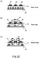
- FIG. 22 is a view showing a cross-section in a plane perpendicular to the substrate 15 of the coupled line 300 shown in FIG. 20 .
- curves with arrows represent lines of electric force.
- the even mode, the odd mode, and the mixed mode are determined depending upon the distribution of the electric polarity of lines included in a coupled line.
- FIG. 22(a) shows the state of an electric field in an even mode.
- the electric potentials of three lines 41, 42, and 43 with respect to the ground 32 are all positive. More specifically, three lines 41, 42, and 43 all have the same electric polarity. Even when the electric polarities of three lines are all negative, the electric field also is in an even mode.
- FIG. 22(b) shows the state of an electric potential in an odd mode.
- the electric potential of the first line 41 is positive with respect to the ground 32
- the electric potential of the second line 42 is the same as that of the ground 32
- the electric potential of the third line 43 is negative with respect to the ground 32.
- electric polarities are distributed so that the electric polarities of the two lines at both ends among three lines are opposite to the electric polarity of the line at the center.
- FIG. 22(c) shows the state of an electric field in a mixed mode.
- the electric potential of the first line 41 is positive with respect to the ground 32
- the electric potential of the second line 42 is negative with respect to the ground 32
- the electric potential of the third line 43 is positive with respect to the ground 32.
- the electric polarities are distributed so that each electric polarity of the three lines is opposite to that of the adjacent line.
- ⁇ ee R ee + j ⁇ L ee G ee + j ⁇ C ee
- Z ee R ee + j ⁇ L ee G ee + j ⁇ C ee
- R oo , L oo , G oo , and C oo have the following meanings:
- R oe , L oe , G oe , and C oe have the following meanings:
- ⁇ means the angular frequency of a transmission line.
- the RLGC parameters in each mode: an even mode, an odd mode, and a mixed mode are calculated, for example, using line information that is data representing the configuration of a transmission line included in a coupled line.
- S parameters per unit length of each transmission line are obtained regarding the coupled lines with various configurations.
- RLGC parameters in each mode an even mode, an odd mode, and a mixed mode with respect to the configuration of the coupled line can be calculated. More specifically, RLGC parameters in each of an even mode, an odd mode, and a mixed mode of a coupled line having a configuration specified by line information can be calculated from line information representing the configuration of the coupled line and S parameters per unit length of a transmission line constituting the coupled line. Thus, RLGC parameters can be calculated with respect to coupled lines with various configurations. The calculated RLGC parameters are recorded, for example, in the RLGC parameter recording unit 104 shown in FIG. 1 .
- the circuit equation of the equivalent circuit shown in FIG. 21 is solved using these circuit matrices and the ASPs obtained in the above Expressions 18-20, whereby S parameters of an S matrix of the equivalent circuit shown in FIG. 21 are obtained. Consequently, S parameters of an S matrix of the coupled line 300 at a frequency "f" are obtained from the RLGC parameters in an even mode, an odd mode, and a mixed mode, the frequency " ⁇ ", the ASP1, the ASP2, and the ASP3.
- S parameters of an S matrix of a coupled line including three lines are calculated.
- the interference among three wires as well as the interference between two wires can be analyzed.
- FIG. 23 shows an exemplary configuration of a coupled line including three lines.
- FIGS. 23(a) and 23(b) are views showing a cross-section in a plane perpendicular to a substrate of a coupled line including three lines.
- the examples shown in FIGS. 23(a) and 23(b) are the cases where a coupled line is composed of lines provided on different layers of a multi-layered board.
- FIG. 23(a) and 23(b) are the cases where a coupled line is composed of lines provided on different layers of a multi-layered board.
- a first line 41a and a second line 42a are provided on the same layer, and a third line 43a is provided on an underlying layer. Furthermore, in FIG. 23(b) , the first line 41b, the second line 42b, and the third line 43b are provided on three different layers. The second line 42b is placed so as to overlap the first line 41b and the third line 43b in upper and lower directions in the figure.
- the second line 42b may be a ground. More specifically, a circuit matrix of a coupled line can be calculated, dealing with the ground as a line constituting the coupled line. Consequently, the interference even including the influence of the ground as well as the interference in one line can be analyzed. This enhances the precision of the analysis.
- the interference analysis device may calculate a circuit matrix with respect to a coupled line including at least three lines.
- the present invention is useful as an interference analysis device capable of shortening a processing time significantly while maintaining high precision, and can shorten a time taken for wiring design of a circuit board substantially.
Landscapes
- Engineering & Computer Science (AREA)
- Computer Hardware Design (AREA)
- Physics & Mathematics (AREA)
- Theoretical Computer Science (AREA)
- Microelectronics & Electronic Packaging (AREA)
- Evolutionary Computation (AREA)
- Geometry (AREA)
- General Engineering & Computer Science (AREA)
- General Physics & Mathematics (AREA)
- Design And Manufacture Of Integrated Circuits (AREA)
- Management, Administration, Business Operations System, And Electronic Commerce (AREA)
Claims (10)
- Dispositif d'analyse d'interférence (10) pour analyser une interférence entre des fils prévus sur une carte de circuit et comprenant une ligne couplée, comprenant:une unité d'entrée (2) qui entre des données de conception représentant un agencement des fils sur la carte de circuit,une unité de sélection (3) qui sélectionne, en tant que zone d'analyse, au moins une partie de la carte de circuit représentée par les données de conception,une unité de division (5) qui divise les fils dans la zone d'analyse en segments servant d'unités destinées à calculer une matrice de circuit,une unité de calcul (6) qui calcule une matrice de circuit par rapport à une ligne couplée constituée par une pluralité de segments adjacents les uns aux autres parmi les segments divisés par l'unité de division,une unité d'analyse (7) qui obtient un degré d'interférence électromagnétique entre les fils dans la zone d'analyse sur la base de la matrice de circuit,caractérisé par le fait que l'unité de calcul (6) calcule la matrice de circuit de la ligne couplée, en utilisant un paramètre d'asymétrie ASP représentant une asymétrie de la ligne couplée et des paramètres RLGC contenant une résistance (R), une inductance (L), une conductance parallèle (G) et une capacité (C) d'une ligne de transmission dans la ligne couplée,dans lequel le paramètre d'asymétrie interpole une asymétrie de la ligne couplée asymétrique pour permettre à la ligne couplée asymétrique d'être traitée comme une ligne couplée symétrique en faisant tourner la matrice de circuit de manière mathématique selon un angle θ - π/4, dans lequel tan Θ = ASP de sorte qu'un mode impair et un mode pair présentent une relation symétrique de 1 : 1 dans la ligne couplée asymétrique,dans lequel le paramètre d'asymétrie est calculé par l'expression suivante dans une ligne couplée constituée par une première ligne et une deuxième ligne:

- Dispositif d'analyse d'interférence (10) selon la revendication 1,
dans lequel des paramètres d'asymétrie ASP1, ASP2 et ASP3 dans une ligne couplée constituée par une première ligne, une deuxième ligne et une troisième ligne et ayant une configuration dans laquelle une distance entre la première ligne et la troisième ligne est supérieure à une distance entre les autres ensembles de deux lignes sont calculés respectivement par les expressions suivantes, et
l'unité de calcul (6) calcule une matrice de circuit de la ligne couplée, en utilisant ASP1, ASP2 et ASP3 en tant que paramètres d'asymétrie:


- Dispositif d'analyse d'interférence (10) selon la revendication 1,
dans lequel l'unité de division (5) divise deux fils qui sont présents dans la zone d'analyse de manière à être adjacents l'un à l'autre de telle sorte qu'une position constituant une limite entre une portion où les deux fils sont disposés en parallèle et une portion où les deux fils ne sont pas disposés en parallèle est incluse dans une limite des segments. - Dispositif d'analyse d'interférence (10) selon la revendication 1,
dans lequel la matrice de circuit est une matrice S. - Dispositif d'analyse d'interférence (10) selon la revendication 1,
comprenant en outre une unité d'enregistrement (9) stockant une pluralité d'ensembles de paramètres obtenus respectivement en ajoutant un paramètre d'asymétrie représentant une asymétrie de la ligne couplée à des paramètres RLGC contenant une résistance (R), une inductance (L), une conductance parallèle (G), et une capacité (C) d'une ligne de transmission dans la ligne couplée,
dans lequel, dans l'unité d'enregistrement (9), les ensembles de paramètres sont enregistrés de manière à être associés à de l'information de ligne représentant des configurations de lignes couplées concernant les ensembles de paramètres, et,
en ce qui concerne une ligne couplée dans la zone d'analyse, l'unité de calcul (6) recherche, dans l'unité d'enregistrement, de l'information de ligne adaptée à la configuration de la ligne couplée, et calcule une matrice de circuit de la ligne couplée en utilisant un ensemble de paramètres correspondant à l'information de ligne obtenue en tant résultat de la recherche. - Dispositif d'analyse d'interférence (10) selon la revendication 5,
dans lequel, dans un cas où l'unité de calcul (6) n'est pas capable d'obtenir l'ensemble de paramètres correspondant en tant que résultat de la recherche, l'unité de calcul (6) effectue une interpolation en utilisant un ensemble de paramètres d'information de ligne proche d'une configuration de la ligne couplée concernant la recherche, obtenant ainsi un ensemble de paramètres dans la ligne couplée. - Dispositif d'analyse d'interférence (10) selon la revendication 1,
dans lequel l'unité de calcul (6) calcule une matrice de circuit de la ligne couplée concernant une pluralité de fréquences différentes, en utilisant un paramètre d'asymétrie représentant une asymétrie de la ligne couplée et des paramètres RLGC contenant une résistance (R), une inductance (L), une conductance parallèle (G) et une capacité (C) d'une ligne de transmission dans la ligne couplée. - Dispositif d'analyse d'interférence (10) selon la revendication 1, comprenant en outre:une unité d'établissement de condition (1) qui établit une condition d'analyse d'interférence contenant une valeur de référence de quantité d'interférence;une unité de sélection de paire (4) qui sélectionne une paire de fils à analyser parmi des fils dans la zone d'analyse,une unité de calcul de quantité d'interférence (71) qui calcule une quantité d'interférence entre la paire de fils sur la base d'une condition de connexion représentant une relation de connexion entre des segments inclus dans la paire de fils et la matrice de circuit calculée dans l'unité de calcul (6), etune unité de jugement (72) qui juge si une interférence entre la paire de fils cause un problème, en comparant la valeur de référence de quantité d'interférence à la quantité d'interférence.
- Procédé d'analyse d'interférence implémenté par ordinateur pour analyser une interférence entre des fils prévus sur une carte de circuit et comprenant une ligne couplée, le procédé comprenant:un traitement d'entrée consistant à entrer des données de conception représentant un agencement de fils sur la carte de circuit,un traitement de sélection (S10) consistant à sélectionner, en tant que zone d'analyse, au moins une partie de la carte de circuit représentée par les données de conception,un traitement de division (S20) consistant à diviser les fils dans la zone d'analyse en segments servant d'unités destinées à calculer une matrice de circuit,un traitement de calcul (S30) consistant à calculer une matrice de circuit par rapport à une ligne couplée constituée par une pluralité de segments adjacents les uns aux autres parmi les segments divisés par le traitement de division, etun traitement d'analyse (S40) consistant à obtenir un degré d'interférence électromagnétique entre les fils dans la zone d'analyse sur la base de la matrice de circuit,caractérisé par le fait que le traitement de calcul (S30) calcule une matrice de circuit de la ligne couplée, en utilisant un paramètre d'asymétrie ASP représentant une asymétrie de la ligne couplée et des paramètres RLGC contenant une résistance (R), une inductance (L), une conductance parallèle (G) et une capacité (C) d'une ligne de transmission dans la ligne couplée,dans lequel le paramètre d'asymétrie interpole une asymétrie de la ligne couplée asymétrique pour permettre à la ligne couplée asymétrique d'être traitée comme une ligne couplée symétrique en faisant tourner la matrice de circuit de manière mathématique selon un angle o - π/4, dans lequel tan Θ = ASP de sorte qu'un mode impair et un mode pair présentent une relation symétrique de 1 : 1 dans la ligne couplée asymétrique,dans lequel le paramètre d'asymétrie (ASP) est calculé par l'expression suivante dans une ligne couplée constituée par une première ligne et une deuxième ligne:

- Support d'enregistrement stockant un programme d'analyse d'interférence pour amener un ordinateur à exécuter les étapes d'un procédé d'analyse d'interférence selon la revendication 9, lorsque ledit programme est exécuté sur ledit ordinateur.
Applications Claiming Priority (2)
| Application Number | Priority Date | Filing Date | Title |
|---|---|---|---|
| JP2005118710 | 2005-04-15 | ||
| PCT/JP2006/307969 WO2006112411A1 (fr) | 2005-04-15 | 2006-04-14 | Dispositif d’analyse de brouillage de cablage de circuit, programme d’analyse de brouillage, base de donnees utilisee dans le dispositif d’analyse de brouillage, et modele de ligne connecte asymetriquement |
Publications (3)
| Publication Number | Publication Date |
|---|---|
| EP1876546A1 EP1876546A1 (fr) | 2008-01-09 |
| EP1876546A4 EP1876546A4 (fr) | 2009-06-03 |
| EP1876546B1 true EP1876546B1 (fr) | 2019-04-03 |
Family
ID=37115129
Family Applications (1)
| Application Number | Title | Priority Date | Filing Date |
|---|---|---|---|
| EP06731905.3A Ceased EP1876546B1 (fr) | 2005-04-15 | 2006-04-14 | Dispositif d'analyse de brouillage de cablage de circuit, programme d'analyse de brouillage, base de donnees utilisee dans le dispositif d'analyse de brouillage, et modele de ligne connecte asymetriquement |
Country Status (5)
| Country | Link |
|---|---|
| US (1) | US7814445B2 (fr) |
| EP (1) | EP1876546B1 (fr) |
| JP (1) | JP4660478B2 (fr) |
| CN (1) | CN101160584B (fr) |
| WO (1) | WO2006112411A1 (fr) |
Families Citing this family (14)
| Publication number | Priority date | Publication date | Assignee | Title |
|---|---|---|---|---|
| JP2008116369A (ja) * | 2006-11-06 | 2008-05-22 | Fujitsu Ltd | パラメータ算出装置、方法、及びプログラム |
| EP2040186A4 (fr) * | 2007-01-15 | 2012-08-22 | Panasonic Corp | Dispositif d'analyse pour un dispositif de circuit, procédé d'analyse, programme d'analyse et support électronique |
| CN102279896B (zh) * | 2010-06-10 | 2015-03-25 | 赛恩倍吉科技顾问(深圳)有限公司 | Hspice兼容等效电路仿真系统及方法 |
| CN102044734B (zh) * | 2010-10-18 | 2013-11-13 | 杭州紫光网络技术有限公司 | 高隔离度同系统合路器 |
| WO2014056201A1 (fr) * | 2012-10-12 | 2014-04-17 | Mediatek Inc. | Module de topologie pour carte à circuits imprimés |
| US8904330B2 (en) | 2013-03-15 | 2014-12-02 | Synopsys, Inc. | Phase determination for extraction from scattering parameters |
| JP6267918B2 (ja) * | 2013-10-09 | 2018-01-24 | ローム株式会社 | ノイズ源を含むデバイスの評価方法 |
| WO2015114677A1 (fr) * | 2014-01-28 | 2015-08-06 | 株式会社図研 | Dispositif d'aide à la conception, procédé d'aide à la conception, programme et support mémoire |
| US9715567B1 (en) * | 2014-07-16 | 2017-07-25 | Ansys, Inc. | Systems and methods for full-order equivalent circuit approach (ECA) modeling of layered structures |
| JP6912204B2 (ja) * | 2016-03-18 | 2021-08-04 | ローム株式会社 | コンピュータシミュレーション方法、伝送線路モデルの生成方法 |
| CN106546904B (zh) * | 2016-10-18 | 2019-01-25 | 瑞斯康达科技发展股份有限公司 | 一种确定信号线间串扰信号的方法及系统 |
| CN107977533B (zh) * | 2017-12-21 | 2020-06-16 | 北京华大九天软件有限公司 | 一种集成电路设计中降低方程组计算复杂度的方法 |
| CN117556750B (zh) * | 2023-10-24 | 2024-06-21 | 广东工业大学 | 导线间电磁耦合的快速计算方法、装置、电子设备及介质 |
| CN118656943B (zh) * | 2024-08-16 | 2024-10-22 | 山东省邮电工程有限公司 | 建筑物智能布线系统 |
Family Cites Families (6)
| Publication number | Priority date | Publication date | Assignee | Title |
|---|---|---|---|---|
| EP0845746A3 (fr) | 1996-11-27 | 2001-01-17 | Matsushita Electric Industrial Co., Ltd. | Dispositif CAO pour cartes à circuit imprimé qui détermine les valeurs de paramètre de conception |
| JPH10214281A (ja) | 1996-11-27 | 1998-08-11 | Matsushita Electric Ind Co Ltd | プリント回路基板用cad装置 |
| JP3442603B2 (ja) | 1996-12-20 | 2003-09-02 | 均 西山 | 結合ストリップライン形伝送路の特性決定装置 |
| JPH11296504A (ja) | 1998-04-06 | 1999-10-29 | Hitachi Ltd | 有限要素法と境界要素法との結合による電磁界解析法 |
| JP2004145379A (ja) * | 2002-10-21 | 2004-05-20 | Handotai Rikougaku Kenkyu Center:Kk | 半導体集積回路におけるインダクタンスの計算方法 |
| JP2005044331A (ja) * | 2003-07-09 | 2005-02-17 | Hioki Ee Corp | 伝送線路の分布定数解析装置および同装置用プログラム |
-
2006
- 2006-04-14 EP EP06731905.3A patent/EP1876546B1/fr not_active Ceased
- 2006-04-14 CN CN2006800125937A patent/CN101160584B/zh not_active Expired - Fee Related
- 2006-04-14 US US11/911,609 patent/US7814445B2/en not_active Expired - Fee Related
- 2006-04-14 WO PCT/JP2006/307969 patent/WO2006112411A1/fr not_active Ceased
- 2006-04-14 JP JP2006522166A patent/JP4660478B2/ja not_active Expired - Fee Related
Non-Patent Citations (2)
| Title |
|---|
| BRANDAO FARIO J A ET AL: "ON THE MODAL ANALYSIS OF ASYMMETRICAL THREE-PHASE TRANSMISSION LINES USING STANDARD TRANSFORMATION MATRICES", IEEE TRANSACTIONS ON POWER DELIVERY, IEEE SERVICE CENTER, NEW YORK, NY, US, vol. 12, no. 4, 1 October 1997 (1997-10-01), pages 1760 - 1765, XP011049385, ISSN: 0885-8977, DOI: 10.1109/61.634202 * |
| VIJAI K TRIPATHI: "Asymmetric Coupled Transmission Lines in an Inhomogeneous Medium", IEEE TRANSACTIONS ON MICROWAVE THEORY AND TECHNIQUES,, vol. MTT-23, no. 9, 1 September 1975 (1975-09-01), pages 734 - 739, XP001367161 * |
Also Published As
| Publication number | Publication date |
|---|---|
| JP4660478B2 (ja) | 2011-03-30 |
| EP1876546A4 (fr) | 2009-06-03 |
| CN101160584A (zh) | 2008-04-09 |
| JPWO2006112411A1 (ja) | 2008-12-11 |
| US20090019403A1 (en) | 2009-01-15 |
| CN101160584B (zh) | 2012-08-22 |
| WO2006112411A1 (fr) | 2006-10-26 |
| US7814445B2 (en) | 2010-10-12 |
| EP1876546A1 (fr) | 2008-01-09 |
Similar Documents
| Publication | Publication Date | Title |
|---|---|---|
| Cangellaris et al. | Electromagnetic model order reduction for system-level modeling | |
| Li | Electrical Modeling and Design for 3D System Integration: 3D Integrated Circuits and Packaging, Signal Integrity, Power Integrity and EMC | |
| EP1876546A1 (fr) | Dispositif d'analyse de brouillage de cablage de circuit, programme d'analyse de brouillage, base de donnees utilisee dans le dispositif d'analyse de brouillage, et modele de ligne connecte asymetriquement | |
| US8024692B2 (en) | Modeling the skin effect using efficient conduction mode techniques | |
| US8200445B2 (en) | Power supply noise analysis method, system and program for electronic circuit board | |
| Melcón et al. | Efficient CAD of boxed microwave circuits based on arbitrary rectangular elements | |
| Mehrotra | Modeling the effects of systematic process variation of circuit performance | |
| Xue et al. | Rapid modeling and simulation of integrated circuit layout in both frequency and time domains from the perspective of inverse | |
| US8132140B2 (en) | Analyzing device for circuit device, circuit device analyzing method, analyzing program, and electronic medium | |
| US9507906B2 (en) | Metal interconnect modeling | |
| Ferranti et al. | Physics-based passivity-preserving parameterized model order reduction for PEEC circuit analysis | |
| Antonini | A new methodology for the transient analysis of lossy and dispersive multiconductor transmission lines | |
| Lee et al. | A quadratic eigenvalue solver of linear complexity for 3-D electromagnetics-based analysis of large-scale integrated circuits | |
| Cangellaris et al. | Model order reduction techniques for electromagnetic macromodelling based on finite methods | |
| Rong et al. | Interconnect transient simulation in the presence of layout and routing uncertainty | |
| Kolstad et al. | A new circuit augmentation method for modeling of interconnects and passive components | |
| Mohan et al. | Causal reduced-order modeling of distributed structures in a transient circuit simulator | |
| Kapur et al. | Modeling of integrated RF passive devices | |
| Zhu et al. | Eliminating the low-frequency breakdown problem in 3-D full-wave finite-element-based analysis of integrated circuits | |
| Su et al. | Application of two-dimensional nonuniform fast Fourier transform (2-D NUFFT) technique to analysis of shielded microstrip circuits | |
| Li et al. | Quasi‐static numerical modeling of miniature RF circuits based on lumped equivalent circuits | |
| Shilimkar et al. | Scalable modeling of on-chip spiral inductors including metal fill parasitics | |
| Rimolo-Donadio | Development, validation, and application of semi-analytical interconnect models for efficient simulation of multilayer substrates | |
| Ferranti et al. | Parametric macromodeling of lossy and dispersive multiconductor transmission lines | |
| Avula et al. | A novel iterative method for approximating frequency response with equivalent pole/residues |
Legal Events
| Date | Code | Title | Description |
|---|---|---|---|
| PUAI | Public reference made under article 153(3) epc to a published international application that has entered the european phase |
Free format text: ORIGINAL CODE: 0009012 |
|
| 17P | Request for examination filed |
Effective date: 20071115 |
|
| AK | Designated contracting states |
Kind code of ref document: A1 Designated state(s): DE FR GB |
|
| DAX | Request for extension of the european patent (deleted) | ||
| RBV | Designated contracting states (corrected) |
Designated state(s): DE FR GB |
|
| RAP1 | Party data changed (applicant data changed or rights of an application transferred) |
Owner name: PANASONIC CORPORATION |
|
| A4 | Supplementary search report drawn up and despatched |
Effective date: 20090508 |
|
| 17Q | First examination report despatched |
Effective date: 20090924 |
|
| RAP1 | Party data changed (applicant data changed or rights of an application transferred) |
Owner name: PANASONIC INTELLECTUAL PROPERTY MANAGEMENT CO., LT |
|
| STAA | Information on the status of an ep patent application or granted ep patent |
Free format text: STATUS: EXAMINATION IS IN PROGRESS |
|
| REG | Reference to a national code |
Ref country code: DE Ref legal event code: R079 Ref document number: 602006057702 Country of ref document: DE Free format text: PREVIOUS MAIN CLASS: G06F0017500000 Ipc: H05K0001020000 |
|
| RIC1 | Information provided on ipc code assigned before grant |
Ipc: H05K 1/02 20060101AFI20180813BHEP Ipc: G06F 17/50 20060101ALI20180813BHEP Ipc: H05K 3/00 20060101ALI20180813BHEP |
|
| GRAP | Despatch of communication of intention to grant a patent |
Free format text: ORIGINAL CODE: EPIDOSNIGR1 |
|
| STAA | Information on the status of an ep patent application or granted ep patent |
Free format text: STATUS: GRANT OF PATENT IS INTENDED |
|
| INTG | Intention to grant announced |
Effective date: 20181016 |
|
| GRAS | Grant fee paid |
Free format text: ORIGINAL CODE: EPIDOSNIGR3 |
|
| GRAA | (expected) grant |
Free format text: ORIGINAL CODE: 0009210 |
|
| STAA | Information on the status of an ep patent application or granted ep patent |
Free format text: STATUS: THE PATENT HAS BEEN GRANTED |
|
| AK | Designated contracting states |
Kind code of ref document: B1 Designated state(s): DE FR GB |
|
| REG | Reference to a national code |
Ref country code: GB Ref legal event code: FG4D |
|
| REG | Reference to a national code |
Ref country code: DE Ref legal event code: R096 Ref document number: 602006057702 Country of ref document: DE |
|
| PGFP | Annual fee paid to national office [announced via postgrant information from national office to epo] |
Ref country code: DE Payment date: 20190418 Year of fee payment: 14 |
|
| REG | Reference to a national code |
Ref country code: DE Ref legal event code: R097 Ref document number: 602006057702 Country of ref document: DE |
|
| PLBE | No opposition filed within time limit |
Free format text: ORIGINAL CODE: 0009261 |
|
| STAA | Information on the status of an ep patent application or granted ep patent |
Free format text: STATUS: NO OPPOSITION FILED WITHIN TIME LIMIT |
|
| 26N | No opposition filed |
Effective date: 20200106 |
|
| GBPC | Gb: european patent ceased through non-payment of renewal fee |
Effective date: 20190703 |
|
| PG25 | Lapsed in a contracting state [announced via postgrant information from national office to epo] |
Ref country code: GB Free format text: LAPSE BECAUSE OF NON-PAYMENT OF DUE FEES Effective date: 20190703 |
|
| PG25 | Lapsed in a contracting state [announced via postgrant information from national office to epo] |
Ref country code: FR Free format text: LAPSE BECAUSE OF NON-PAYMENT OF DUE FEES Effective date: 20190603 |
|
| REG | Reference to a national code |
Ref country code: DE Ref legal event code: R119 Ref document number: 602006057702 Country of ref document: DE |
|
| PG25 | Lapsed in a contracting state [announced via postgrant information from national office to epo] |
Ref country code: DE Free format text: LAPSE BECAUSE OF NON-PAYMENT OF DUE FEES Effective date: 20201103 |