EP1876647A2 - Rückbeleuchteter Bildsensor - Google Patents
Rückbeleuchteter Bildsensor Download PDFInfo
- Publication number
- EP1876647A2 EP1876647A2 EP07111519A EP07111519A EP1876647A2 EP 1876647 A2 EP1876647 A2 EP 1876647A2 EP 07111519 A EP07111519 A EP 07111519A EP 07111519 A EP07111519 A EP 07111519A EP 1876647 A2 EP1876647 A2 EP 1876647A2
- Authority
- EP
- European Patent Office
- Prior art keywords
- layer
- face
- image sensor
- dopant concentration
- photodiode
- Prior art date
- Legal status (The legal status is an assumption and is not a legal conclusion. Google has not performed a legal analysis and makes no representation as to the accuracy of the status listed.)
- Withdrawn
Links
Images
Classifications
-
- H—ELECTRICITY
- H10—SEMICONDUCTOR DEVICES; ELECTRIC SOLID-STATE DEVICES NOT OTHERWISE PROVIDED FOR
- H10F—INORGANIC SEMICONDUCTOR DEVICES SENSITIVE TO INFRARED RADIATION, LIGHT, ELECTROMAGNETIC RADIATION OF SHORTER WAVELENGTH OR CORPUSCULAR RADIATION
- H10F39/00—Integrated devices, or assemblies of multiple devices, comprising at least one element covered by group H10F30/00, e.g. radiation detectors comprising photodiode arrays
- H10F39/011—Manufacture or treatment of image sensors covered by group H10F39/12
- H10F39/014—Manufacture or treatment of image sensors covered by group H10F39/12 of CMOS image sensors
-
- H—ELECTRICITY
- H10—SEMICONDUCTOR DEVICES; ELECTRIC SOLID-STATE DEVICES NOT OTHERWISE PROVIDED FOR
- H10F—INORGANIC SEMICONDUCTOR DEVICES SENSITIVE TO INFRARED RADIATION, LIGHT, ELECTROMAGNETIC RADIATION OF SHORTER WAVELENGTH OR CORPUSCULAR RADIATION
- H10F39/00—Integrated devices, or assemblies of multiple devices, comprising at least one element covered by group H10F30/00, e.g. radiation detectors comprising photodiode arrays
- H10F39/10—Integrated devices
- H10F39/12—Image sensors
- H10F39/18—Complementary metal-oxide-semiconductor [CMOS] image sensors; Photodiode array image sensors
-
- H—ELECTRICITY
- H10—SEMICONDUCTOR DEVICES; ELECTRIC SOLID-STATE DEVICES NOT OTHERWISE PROVIDED FOR
- H10F—INORGANIC SEMICONDUCTOR DEVICES SENSITIVE TO INFRARED RADIATION, LIGHT, ELECTROMAGNETIC RADIATION OF SHORTER WAVELENGTH OR CORPUSCULAR RADIATION
- H10F39/00—Integrated devices, or assemblies of multiple devices, comprising at least one element covered by group H10F30/00, e.g. radiation detectors comprising photodiode arrays
- H10F39/10—Integrated devices
- H10F39/12—Image sensors
- H10F39/199—Back-illuminated image sensors
-
- H—ELECTRICITY
- H10—SEMICONDUCTOR DEVICES; ELECTRIC SOLID-STATE DEVICES NOT OTHERWISE PROVIDED FOR
- H10F—INORGANIC SEMICONDUCTOR DEVICES SENSITIVE TO INFRARED RADIATION, LIGHT, ELECTROMAGNETIC RADIATION OF SHORTER WAVELENGTH OR CORPUSCULAR RADIATION
- H10F39/00—Integrated devices, or assemblies of multiple devices, comprising at least one element covered by group H10F30/00, e.g. radiation detectors comprising photodiode arrays
- H10F39/80—Constructional details of image sensors
- H10F39/803—Pixels having integrated switching, control, storage or amplification elements
-
- H—ELECTRICITY
- H10—SEMICONDUCTOR DEVICES; ELECTRIC SOLID-STATE DEVICES NOT OTHERWISE PROVIDED FOR
- H10F—INORGANIC SEMICONDUCTOR DEVICES SENSITIVE TO INFRARED RADIATION, LIGHT, ELECTROMAGNETIC RADIATION OF SHORTER WAVELENGTH OR CORPUSCULAR RADIATION
- H10F39/00—Integrated devices, or assemblies of multiple devices, comprising at least one element covered by group H10F30/00, e.g. radiation detectors comprising photodiode arrays
- H10F39/011—Manufacture or treatment of image sensors covered by group H10F39/12
- H10F39/026—Wafer-level processing
-
- H—ELECTRICITY
- H10—SEMICONDUCTOR DEVICES; ELECTRIC SOLID-STATE DEVICES NOT OTHERWISE PROVIDED FOR
- H10F—INORGANIC SEMICONDUCTOR DEVICES SENSITIVE TO INFRARED RADIATION, LIGHT, ELECTROMAGNETIC RADIATION OF SHORTER WAVELENGTH OR CORPUSCULAR RADIATION
- H10F39/00—Integrated devices, or assemblies of multiple devices, comprising at least one element covered by group H10F30/00, e.g. radiation detectors comprising photodiode arrays
- H10F39/80—Constructional details of image sensors
- H10F39/805—Coatings
- H10F39/8053—Colour filters
-
- H—ELECTRICITY
- H10—SEMICONDUCTOR DEVICES; ELECTRIC SOLID-STATE DEVICES NOT OTHERWISE PROVIDED FOR
- H10F—INORGANIC SEMICONDUCTOR DEVICES SENSITIVE TO INFRARED RADIATION, LIGHT, ELECTROMAGNETIC RADIATION OF SHORTER WAVELENGTH OR CORPUSCULAR RADIATION
- H10F39/00—Integrated devices, or assemblies of multiple devices, comprising at least one element covered by group H10F30/00, e.g. radiation detectors comprising photodiode arrays
- H10F39/80—Constructional details of image sensors
- H10F39/806—Optical elements or arrangements associated with the image sensors
- H10F39/8063—Microlenses
Definitions
- the present invention relates to the field of image sensors for use in mobile phones, cameras, camcorders or digital cameras. It relates more particularly to image sensors made monolithically based on semiconductor materials.
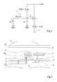
- Figure 1 schematically illustrates an exemplary circuit of a photosensitive cell of a matrix of photosensitive cells of an image sensor.
- Each photosensitive cell of the matrix is associated with a precharging device and a reading device.
- the precharging device consists of an NM channel NM transistor 1 , interposed between a supply rail Vdd and a read node S.
- the gate of the precharge transistor M 1 is adapted to receive a precharge control signal RST .
- the reading device consists of the series connection of first and second MOS transistors with channel NM 2 , M 3 .
- the drain of the first read transistor M 2 is connected to the supply rail Vdd.
- the source of the second read transistor M 3 is connected to an input terminal P of a processing circuit (not shown).
- the gate of the first read transistor M 2 is connected to the read node S.
- the gate of the second read transistor M 3 is adapted to receive a read signal RD.
- the photosensitive cell comprises a charge storage diode D 1 whose anode is connected to a source of a reference potential or ground of the GND circuit and the cathode is connected directly to the node S.
- the photosensitive cell comprises a photodiode D 2 whose anode is connected to the reference supply rail GND and the cathode is connected to the node S via an MOS transistor N-channel charge transfer M 4 .
- the gate of the transfer transistor M 4 is adapted to receive a charge transfer control signal T.
- the signals RD, RST, and T are provided by control circuits not shown in FIG.
- the diode D 1 may not be realized by a specific component.
- the storage function of the charges coming from the photodiode D 2 is then ensured by the apparent capacitance at the reading node S which consists of the capacitances of the sources of the transistors M 1 and M 4 , the input capacitance of the transistor M 2 and than all the parasitic capacitances present at the node S.
- a photodetection cycle begins with a precharge phase during which a reference voltage level is imposed on the diode D 1 .
- This precharging is carried out by passing the precharging transistor M 1 .
- the precharge transistor M 1 is blocked.
- the state is then read at the node S, ie the actual reference state of charge of the diode D 1 .
- the cycle is continued by a transfer to the node S photogenerated charges, that is to say, created and stored in the presence of radiation, in the photodiode D 2 . This transfer is carried out by passing the transfer transistor M 4 .
- FIG. 2 schematically illustrates a photosensitive cell or pixel of a conventional image sensor intended to be illuminated by the front face. Only the photodiode D 2 and the transistor M 4 are represented.
- a substrate 1 of P type - there is provided a region 2 of P-type more highly doped than the substrate 1 and a doped region 3 N pinched between the region 2 and the substrate 1 corresponding to the photodiode D 2 which has a structure said pinch.
- the cell comprises a portion of polycrystalline silicon 4 disposed on an insulating portion 6, spacers 7 being provided on either side of the portions 4, 6.
- the polycrystalline silicon portion 4 corresponds to the gate of the transistor M 4 and the portion insulator 6 corresponds to the gate oxide of transistor M 4 .
- an N-type region 8 corresponding to the reading node of the photosensitive cell.
- Metal interconnections in the form of tracks and metal vias 9, are formed at a stack of insulating layers 11 covering the substrate 1 and are connected to the components of the cell.
- the cell also comprises a color filter 12 covering the stack of insulating layers 11 on which a microlens 13 is disposed.
- the light rays that reach the microlens 13 are focused towards the photodiode D 2 .
- incident light rays can be deflected or blocked by the interconnections 9 and not reach the photodiode D 2 .
- the current trend is to reduce the size of the photosensitive cells, the problem of the presence of metal interconnections 9 becomes even more important. To overcome this problem, it has been imagined a lighting of the photodiode D 2 by the rear face of the substrate 1.
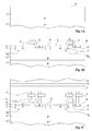
- FIGS. 3A to 3D schematically illustrate steps of an exemplary conventional method of manufacturing an image sensor illuminated by the rear face.
- FIG. 3A shows a strongly doped P-type substrate 14 on which a P-type monocrystalline silicon layer 15 has been epitaxially grown which is less heavily doped than the substrate 14.
- the layer 15 comprises a front face 16 and a, by for example, a thickness of about 3 microns.
- FIG. 3B represents the structure obtained after having made at the level of the layer 15 the components associated with the pixels. In FIG. 3B, two adjacent pixels are represented. The elements common to the pixel represented in FIG. 2 are designated with the same references. To insure the insulation between the two pixels, an insulation zone 17 has been formed in the layer 15, for example made of silicon oxide.
- FIG. 3A shows a strongly doped P-type substrate 14 on which a P-type monocrystalline silicon layer 15 has been epitaxially grown which is less heavily doped than the substrate 14.
- the layer 15 comprises a front face 16 and a, by for
- FIG. 3C represents the structure obtained after having made the levels of interconnections 9 in the stack of insulating layers 11 covering the layer 15 and after having stuck on the stack of insulating layers 11 a second substrate 18 on which it has grown a silicon oxide layer 19.
- FIG. 3D represents the structure obtained after removing the substrate 14, for example by a chemical-mechanical polishing process, to define a rear face 20 of the layer 15 and after having realized on the rear face 20 of the color filters 21 and 22 and microlenses 23 and 24.
- a disadvantage of the image sensor structure shown in FIG. 3D results from the scattering of electrons in the layer 15.
- the incident photons cause the formation in the electron / hole pair layer 15, the electrons forming in a portion of the layer 15 associated with a photosensitive cell to be captured by the photodiode of this cell.
- certain electrons resulting from the absorption of photons in a portion of the layer 15 associated with a cell photosensitive data can be captured by the photodiodes of adjacent photosensitive cells. This results in undesirable noise on the signals measured at the reading nodes whose amplitude varies for each photosensitive cell.
- Such a phenomenon is due to the scattering of electrons forming in a portion of the layer 15 associated with a given photosensitive cell to the photodiodes of adjacent cells rather than to the photodiode of the given photosensitive cell.
- the risk of diffusion of electrons towards adjacent cells is all the more important as the place of formation of the electrons is remote from the photodiodes.
- the photons whose wavelengths correspond to blue or green are mainly absorbed in the first two micrometers of the substrate 1. Due to the focusing of the light rays by the lens 13, the electrons resulting from the absorption of such photons are formed mainly near the photodiode D 2 . The risk that some of these electrons diffuse to the adjacent photosensitive cells is therefore low. Only the photons whose wavelength corresponds to red can be absorbed over a greater thickness of the substrate 1. The risk that some of these electrons diffuse towards the adjacent cells is then greater, but the overall number of electrons likely to spread to adjacent cells remains weak.
- the risk of diffusion of electrons towards the adjacent photosensitive cells is greater.
- the electrons that are most likely to diffuse to the adjacent photosensitive cells are those that form in the first two micrometers of the layer 15 from the rear face 20.
- the number of these electrons is greater than for a sensor images illuminated by the front as they come from the absorption of photons corresponding to blue, green and red colors.
- the disturbance of the signals measured due to the diffusion of electrons towards the adjacent photosensitive cells is therefore more important for a rear-illuminated image sensor.
- An object of the present invention is to provide an image sensor illuminated by the rear face to reduce or eliminate the diffusion of electrons associated with a given pixel to adjacent pixels.
- Another object of the present invention is to provide a method of manufacturing an image sensor illuminated by the rear face to reduce or eliminate the diffusion of electrons associated with a given pixel to adjacent pixels.
- one aspect of the present invention provides an image sensor comprising a layer of a P-type doped semiconductor material having first and second opposing faces; and at least one photodiode formed in the layer on the side of the first face and intended to be illuminated by the second face.
- the dopant concentration of the layer increases from the first face to the second face.
- the increase in the dopant concentration of the layer is substantially continuous.
- the dopant concentration of the layer increases in successive stages.
- the dopant concentration of the layer is substantially constant over a given thickness from the first face.
- the thickness given is 1 ⁇ m.
- the thickness of the layer is between 2 microns and 4 microns.
- Another aspect of the present invention provides a device, in particular a mobile phone, a camera, a camcorder, a digital microscope or a digital camera, comprising an image sensor as previously defined.
- Another aspect of the present invention provides a method of manufacturing an image sensor comprising the steps of forming a layer of a P-type doped semiconductor material having first and second opposing faces, the dopant concentration. the layer increasing from the first face to the second face; and forming in the layer at least one photodiode on the side of the first face and intended to be illuminated by the second face.
- the layer is formed by epitaxy.
- the layer is formed on an insulating layer covering a substrate, the substrate and at least a portion of said insulating layer being removed after forming said photodiode.
- FIG. 4 is a figure similar to FIG. 3D and represents an exemplary embodiment of an image sensor according to the invention.
- the lightly doped P-type layer 15 has been replaced by a p-type doped silicon layer 26 whose dopant concentration increases from the front face 16 of the layer 26 to the 20.
- the thickness of the layer 26 may vary between 2 microns and 6 microns and the dopant concentration may vary from a few 14 atoms / cm 3 near the front face 16 to a few 10 17 atoms / cm 3 near the back face 20.
- the dopant used is of type P, and corresponds, for example, to boron.
- the arrows 27 illustrate the dopant concentration gradient in the layer 26.
- the manufacturing method of the present exemplary embodiment of the image sensor according to the invention can be analogous to the method previously described in relation to FIGS. 3A to 3D, the layer 26 is produced by epitaxy on the substrate 14. It is then expected, simultaneously with the epitaxial growth of the layer 26, to perform a P-type doping whose concentration increases in the direction of the arrows 27.
- the dopant concentration gradient causes the formation of an electrostatic field in the oriented layer 26 as the concentration gradient. This results in the exercise of a force on the electrons forming in the layer 26 oriented in the direction opposite to the arrows 27. The electrons are thus led to the photodiode D 2 associated with the portion of the layer 26 of the pixel in which they are trained. The electrostatic field thus prevents the electrons from diffusing towards the neighboring pixels.
- the increase in the dopant concentration can be carried out continuously and regularly from the front face 16 to the rear face 20 of the layer 26.
- the increase in the concentration can be straight.
- the dopant concentration in the layer 26 may be constant over a given thickness from the front face 16 of the layer 26 and then increase up to the rear face 20.
- the thickness given may be of the order of 1 ⁇ m. This advantageously makes it possible to maintain the dopant concentration constant at the portions of the layer 26 corresponding to the channel regions of the transistors of the photosensitive cells. Indeed, the electrical focusing of a MOS transistor to optimize its operation is very sensitive and is generally performed considering that the silicon portion in which the transistor is formed has a constant dopant concentration. It may therefore be advantageous to have a constant dopant concentration at each transistor of the photosensitive cell so as not to modify the operating point of this transistor and in particular the transistor channel formation conditions.
- the isolation zone 17 may correspond to a P-type region that is more heavily doped than the layer 26.
- the isolation zone 17 may be formed by one or more implantation steps. It can extend from the front face 16 to the given thickness on which the dopant concentration in the layer 26 is constant.
- the layer 26 it is possible to use, for the formation of the layer 26, a structure of the SOI type (acronym for Silicon On Insulator).
- a structure of the SOI type (acronym for Silicon On Insulator).
- the layer of silicon 26 with a variable dopant concentration can be produced by epitaxy on the tie layer.
- variable dopant concentration layer 26 can then be made by strongly doping the bonding layer on the insulating layer of the SOI structure and by epitaxially growing the layer 26 on the tie layer by constant dopant concentration. During the epitaxy, then, an exo-diffusion of the dopants from the tie layer occurs in the layer 26.
- FIG. 5 illustrates an example of use of the image sensor according to the invention.
- FIG. 5 schematically shows a mobile phone 31 comprising a housing 32 at which a screen 33 and a keyboard 34 are arranged.
- the mobile phone also comprises an image acquisition system 36 comprising an optical system controlling the light rays towards an image sensor according to the invention.
- the present invention is susceptible of various variations and modifications which will be apparent to those skilled in the art.
- the present invention also applies to a photosensitive cell for which several photodiodes are connected to the same reading node.
- the present invention has been described for an image sensor cell in which the precharging device and the reading device have a particular structure, the present invention also applies to a cell for which the The preload or the reading device have a different structure, for example comprise a different number of MOS transistors.
Landscapes
- Solid State Image Pick-Up Elements (AREA)
Applications Claiming Priority (1)
| Application Number | Priority Date | Filing Date | Title |
|---|---|---|---|
| FR0652817 | 2006-07-05 |
Publications (1)
| Publication Number | Publication Date |
|---|---|
| EP1876647A2 true EP1876647A2 (de) | 2008-01-09 |
Family
ID=37814652
Family Applications (1)
| Application Number | Title | Priority Date | Filing Date |
|---|---|---|---|
| EP07111519A Withdrawn EP1876647A2 (de) | 2006-07-05 | 2007-07-02 | Rückbeleuchteter Bildsensor |
Country Status (2)
| Country | Link |
|---|---|
| US (1) | US20080017893A1 (de) |
| EP (1) | EP1876647A2 (de) |
Families Citing this family (5)
| Publication number | Priority date | Publication date | Assignee | Title |
|---|---|---|---|---|
| US7888763B2 (en) * | 2008-02-08 | 2011-02-15 | Omnivision Technologies, Inc. | Backside illuminated imaging sensor with improved infrared sensitivity |
| KR20100000161A (ko) * | 2008-06-24 | 2010-01-06 | 삼성전자주식회사 | 백사이드 일루미네이션 이미지 센서 구조를 얻기 위한얼라인키 형성 방법 |
| JP5269527B2 (ja) * | 2008-08-29 | 2013-08-21 | 株式会社東芝 | 半導体装置 |
| US9048162B2 (en) * | 2012-05-31 | 2015-06-02 | Taiwan Semiconductor Manufacturing Company, Ltd. | CMOS image sensors and methods for forming the same |
| US9859311B1 (en) * | 2016-11-28 | 2018-01-02 | Omnivision Technologies, Inc. | Storage gate protection |
Family Cites Families (5)
| Publication number | Priority date | Publication date | Assignee | Title |
|---|---|---|---|---|
| US6683360B1 (en) * | 2002-01-24 | 2004-01-27 | Fillfactory | Multiple or graded epitaxial wafers for particle or radiation detection |
| JP4211696B2 (ja) * | 2004-06-30 | 2009-01-21 | ソニー株式会社 | 固体撮像装置の製造方法 |
| US8049293B2 (en) * | 2005-03-07 | 2011-11-01 | Sony Corporation | Solid-state image pickup device, electronic apparatus using such solid-state image pickup device and method of manufacturing solid-state image pickup device |
| US7381603B2 (en) * | 2005-08-01 | 2008-06-03 | Semiconductor Components Industries, L.L.C. | Semiconductor structure with improved on resistance and breakdown voltage performance |
| US20070045682A1 (en) * | 2005-08-31 | 2007-03-01 | Hong Sungkwon C | Imager with gradient doped EPI layer |
-
2007
- 2007-06-29 US US11/824,287 patent/US20080017893A1/en not_active Abandoned
- 2007-07-02 EP EP07111519A patent/EP1876647A2/de not_active Withdrawn
Also Published As
| Publication number | Publication date |
|---|---|
| US20080017893A1 (en) | 2008-01-24 |
Similar Documents
| Publication | Publication Date | Title |
|---|---|---|
| EP1883112B1 (de) | Bildsensor, der von der Rückseite beleuchtet wird mit einheitlicher Substrattemperatur | |
| EP2216817B1 (de) | Von hinten beleuchteter halbleiter-bildsensor | |
| EP1873836B1 (de) | Von hinten beleuchtete Bildaufnahmevorrichtung | |
| FR2820883A1 (fr) | Photodiode a grande capacite | |
| EP2587539B1 (de) | CMOS-UTBB-Bildaufnehmer | |
| FR2930676A1 (fr) | Capteur d'image de tres faibles dimensions | |
| EP2786412B1 (de) | Optische detektoreinheit | |
| FR2888989A1 (fr) | Capteur d'images | |
| EP2355156B1 (de) | Fotodiode für Bildsensor | |
| FR2884351A1 (fr) | Procede de fabrication d'un circuit integre comprenant une photodiode et circuit integre correspondant. | |
| FR3100926A1 (fr) | Capteur d'images réalisé en technologie 3D séquentielle | |
| EP1876647A2 (de) | Rückbeleuchteter Bildsensor | |
| EP1231642A1 (de) | Photodetektor mit drei Transistoren | |
| FR2844398A1 (fr) | Photodetecteur d'un capteur d'images | |
| EP2312832B1 (de) | Pixelschaltung in Bildsensor | |
| FR2846147A1 (fr) | Commande d'une cellule photosensible | |
| EP2846357A1 (de) | Fotodetektorvorrichtung mit Halbleiterregionen, die durch eine Potenzialbarriere getrennt sind | |
| FR2934926A1 (fr) | Capteur d'images miniature. | |
| FR2918795A1 (fr) | Capteur d'images a sensibilite amelioree. | |
| FR3046295A1 (fr) | Pixel a eclairement par la face arriere | |
| FR2910710A1 (fr) | Capteur d'image cmos a photodiode piegee a faible tension d'alimentation | |
| EP3163622B1 (de) | Lichtempfindliche logikzelle zur beleuchtung von der vorderseite | |
| FR3083001A1 (fr) | Capteur d'images | |
| EP2909861A1 (de) | Bildsensor mit verbesserter quanteneffizienz bei grossen wellenlängen | |
| EP0434502B1 (de) | Hybrider Photosensor |
Legal Events
| Date | Code | Title | Description |
|---|---|---|---|
| PUAI | Public reference made under article 153(3) epc to a published international application that has entered the european phase |
Free format text: ORIGINAL CODE: 0009012 |
|
| AK | Designated contracting states |
Kind code of ref document: A2 Designated state(s): AT BE BG CH CY CZ DE DK EE ES FI FR GB GR HU IE IS IT LI LT LU LV MC MT NL PL PT RO SE SI SK TR |
|
| AX | Request for extension of the european patent |
Extension state: AL BA HR MK YU |
|
| STAA | Information on the status of an ep patent application or granted ep patent |
Free format text: STATUS: THE APPLICATION HAS BEEN WITHDRAWN |
|
| 18W | Application withdrawn |
Effective date: 20101105 |