EP1876704B1 - Regulierung einer Verstärkervorrichtung - Google Patents
Regulierung einer Verstärkervorrichtung Download PDFInfo
- Publication number
- EP1876704B1 EP1876704B1 EP07111332A EP07111332A EP1876704B1 EP 1876704 B1 EP1876704 B1 EP 1876704B1 EP 07111332 A EP07111332 A EP 07111332A EP 07111332 A EP07111332 A EP 07111332A EP 1876704 B1 EP1876704 B1 EP 1876704B1
- Authority
- EP
- European Patent Office
- Prior art keywords
- signal
- supply voltage
- amplifier
- amplification apparatus
- stage
- Prior art date
- Legal status (The legal status is an assumption and is not a legal conclusion. Google has not performed a legal analysis and makes no representation as to the accuracy of the status listed.)
- Not-in-force
Links
- 230000003321 amplification Effects 0.000 title claims abstract description 61
- 238000003199 nucleic acid amplification method Methods 0.000 title claims abstract description 61
- 230000005540 biological transmission Effects 0.000 claims description 27
- 238000000034 method Methods 0.000 claims description 17
- 230000001105 regulatory effect Effects 0.000 claims description 7
- 238000005516 engineering process Methods 0.000 description 5
- 239000003990 capacitor Substances 0.000 description 4
- 238000001914 filtration Methods 0.000 description 4
- 239000004065 semiconductor Substances 0.000 description 4
- 238000012545 processing Methods 0.000 description 3
- 238000004891 communication Methods 0.000 description 2
- 230000001419 dependent effect Effects 0.000 description 2
- 238000013459 approach Methods 0.000 description 1
- 230000000295 complement effect Effects 0.000 description 1
- 238000005259 measurement Methods 0.000 description 1
- 229910044991 metal oxide Inorganic materials 0.000 description 1
- 150000004706 metal oxides Chemical class 0.000 description 1
- 238000010295 mobile communication Methods 0.000 description 1
Images

Classifications
-
- H—ELECTRICITY
- H03—ELECTRONIC CIRCUITRY
- H03F—AMPLIFIERS
- H03F1/00—Details of amplifiers with only discharge tubes, only semiconductor devices or only unspecified devices as amplifying elements
- H03F1/02—Modifications of amplifiers to raise the efficiency, e.g. gliding Class A stages, use of an auxiliary oscillation
- H03F1/0205—Modifications of amplifiers to raise the efficiency, e.g. gliding Class A stages, use of an auxiliary oscillation in transistor amplifiers
- H03F1/0261—Modifications of amplifiers to raise the efficiency, e.g. gliding Class A stages, use of an auxiliary oscillation in transistor amplifiers with control of the polarisation voltage or current, e.g. gliding Class A
-
- H—ELECTRICITY
- H03—ELECTRONIC CIRCUITRY
- H03F—AMPLIFIERS
- H03F1/00—Details of amplifiers with only discharge tubes, only semiconductor devices or only unspecified devices as amplifying elements
- H03F1/02—Modifications of amplifiers to raise the efficiency, e.g. gliding Class A stages, use of an auxiliary oscillation
- H03F1/0205—Modifications of amplifiers to raise the efficiency, e.g. gliding Class A stages, use of an auxiliary oscillation in transistor amplifiers
-
- H—ELECTRICITY
- H03—ELECTRONIC CIRCUITRY
- H03F—AMPLIFIERS
- H03F3/00—Amplifiers with only discharge tubes or only semiconductor devices as amplifying elements
- H03F3/20—Power amplifiers, e.g. Class B amplifiers, Class C amplifiers
- H03F3/24—Power amplifiers, e.g. Class B amplifiers, Class C amplifiers of transmitter output stages
-
- H—ELECTRICITY
- H03—ELECTRONIC CIRCUITRY
- H03F—AMPLIFIERS
- H03F2200/00—Indexing scheme relating to amplifiers
- H03F2200/108—A coil being added in the drain circuit of a FET amplifier stage, e.g. for noise reducing purposes
-
- H—ELECTRICITY
- H03—ELECTRONIC CIRCUITRY
- H03F—AMPLIFIERS
- H03F2200/00—Indexing scheme relating to amplifiers
- H03F2200/18—Indexing scheme relating to amplifiers the bias of the gate of a FET being controlled by a control signal
-
- H—ELECTRICITY
- H03—ELECTRONIC CIRCUITRY
- H03F—AMPLIFIERS
- H03F2200/00—Indexing scheme relating to amplifiers
- H03F2200/181—A coil being added in the gate circuit of a FET amplifier stage, e.g. for noise reducing purposes
-
- H—ELECTRICITY
- H03—ELECTRONIC CIRCUITRY
- H03F—AMPLIFIERS
- H03F2200/00—Indexing scheme relating to amplifiers
- H03F2200/318—A matching circuit being used as coupling element between two amplifying stages
Definitions
- Embodiments of the present invention relate to an amplification apparatus, and more particular to a transmitter having an amplification apparatus, and a method for regulation of the amplification apparatus.
- a transmitter includes an output amplifier, i.e. an amplification apparatus that boosts the power of a transmission signal to a level sufficient to allow for a reception of the transmission signal by a receiver.
- an output amplifier i.e. an amplification apparatus that boosts the power of a transmission signal to a level sufficient to allow for a reception of the transmission signal by a receiver.
- GSM Global System for Mobile Communication
- UMTS Universal Mobile Telecommunication Standard
- the output amplifier may be subject to strict constraints on linearity and efficiency. If the transmitter is using an amplitude modulation such as 8-PSK modulation used in GSM EDGE (Enhanced Data GSM Environment), the output amplifier has to be arranged so that the output signal is linear in relation to the input signal to avoid a distortion of the output signal.
- amplitude modulation such as 8-PSK modulation used in GSM EDGE (Enhanced Data GSM Environment)
- GSM EDGE Enhanced Data GSM Environment
- the efficiency of the output amplifier is defined by the ratio of an outgoing power level at an output of the output amplifier to the power input into the output amplifier. The lower that ratio the more efficient the input power is brought onto the outgoing signal. This is advantageous if the transmitter is part of a mobile terminal having only limited power resources.
- WO 2005/043748 A1 discloses an amplification apparatus comprising a first amplifier stage and a second amplifier stage, a bias voltage circuitry and a supply voltage circuitry coupled to the first amplifier stage, wherein the supply voltage circuitry is coupled to the bias voltage circuitry.
- US 6,031,417 discloses a switchable biasing device for an analog CMOS differential amplifier providing a supply bias current and a corresponding input bias voltage.
- the biasing device includes a control element having states corresponding to power supply voltages.
- the control element controls a supply bias circuit for supplying a bias current to a differential amplifier at a level corresponding to the power supply voltage represented by a control signal from the control element.
- the bias current is made lower for a low power supply voltage to ensure that current source stage elements of the differential amplifier operate within the saturation region, and higher for a high power supply voltage to ensure sufficient current to maintain slew rates.
- the control element further controls an input bias circuit for providing a DC bias voltage at inputs of the differential amplifier at levels corresponding to the power supply voltage represented by the control signal. The control element thereby operates to select a supply bias current and input bias voltage that are appropriate for the power supply voltage.
- US 6,323,731 B1 discloses the use of dynamic bias control in a switch-mode RF amplifier to achieve an output signal having wide dynamic range.
- a method is disclosed of amplifying an RF signal to produce a valuable output signal having an amplifier including a final amplification stage having a control terminal. The method includes applying to the control terminal of the final amplification stage a drive signal and a bias signal; and varying the bias signal as a function of a desired output power of the valuable output signal.
- the drive signal and the bias signal together cause the final amplification stage to be driven repeatedly between two states, a hard-on state and a hard-off state, without operating in a linear operating region for an appreciable percentage of time, and the final amplification stage is controlled without continuous or frequent measurement and feedback adjustment of the valuable output signal.
- EP 0 539 070 A1 discloses a transmitter switch-on in a dual-mode mobile phone.
- the transmitter is switched on in two or more phases, controlled by the mobile phone microprocessor program.
- the power amplifier sections are switched on in sequence, so that the output power amplifier sections are first switched on by enabling the transmit enable signal. Then the input power amplification sections are switched on by enabling ramp-up signal. Transmission is thereafter enabled by the transmit power control signal being switched on, the amplifiers then output the amplified radio frequency input signal to the duplex circuit transmit terminal.
- Figure 1 illustrates an embodiment of a transmitter having an amplification apparatus according to the present invention. It is understood that such amplification apparatus may be used in any application or circuitry to perform signal amplification.
- the transmitter illustrated in Figure 1 includes a transformer 101 that produces a first amplitude information signal and a phase information signal.
- the transformer 101 produces these signals according to input signals that in various embodiments might be delivered as Cartesian information such as quadrature modulated information or inphase and quadrature signals.
- the ingoing signals may be provided by a baseband unit that includes a microcontroller, a DSP or by any other suitable processing element.
- the input signals are containing information i.e. data to be transmitted by the transmitter via a transmission channel such as a wireless or wireline channel.
- the first amplitude information signal is fed into a first input of a mixer 102.
- the phase information signal is fed into a phase modulator 103.
- the phase modulator 103 modulates the phase information signal on a carrier frequency which is defined by the transmission channel.
- the illustrated transmitter includes a ramping control unit 104 that provides a power control signal that represents the ramping up or ramping down procedure for the transmitter.
- the ramping control unit 104 is connected to a second input of the mixer 102.
- the mixer 102 mixes the first amplitude information signal and the power control signal to produce a second amplitude information signal. The mixing is performed by a digital multiplication of the first amplitude information signal and the power control signal.
- the second amplitude information signal is provided at an output of said mixer 102. This signal includes the amplitude information of the signal to be transmitted and information about the ramping up and/or ramping down of the power level of the transmitter.
- the output of mixer 102 is connected to a digital-to-analog converter 105.
- the digital-to-analog converter 105 converts the second amplitude information signal from a digital form into an analog form of the second amplitude information signal.
- An output of the digital-to-analog converter 105 is connected to a modulator 106.
- An output of the phase modulator 103 is also connected to the modulator 106.
- the modulator 106 modulates the amplitude information signal in its analog form on the phase information signal being shifted on the carrier frequency of the transmission system.
- a signal output 107 of the modulator 106 provides an output signal that includes amplitude information, ramping information and/or phase information.
- the modulator 106 is an amplification apparatus according to an embodiment of the present invention.
- the transmitter illustrated in Figure 1 includes digital signal processing in the transmission path.
- the ramping information is brought on the signal or combined with the signal to be transmitted in the digital domain of the transmitter. This is performed by means of the mixer 102. Yet other suitable approaches may be used.
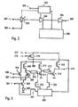
- Figure 2 illustrates an embodiment of an amplification apparatus.
- the amplification apparatus includes a signal input 201 for receiving a radio frequency signal to be transmitted.
- the radio frequency signal is fed by the signal input 201 into a variable gain amplifier stage 202.
- the amplification apparatus includes a second input 203 connected to the variable gain amplifier 202.
- the second input 203 is receiving a gain setting signal fed into the variable gain amplifier stage 202 so as to set a gain of the variable gain amplifier stage 202.
- An output of the variable gain amplifier stage 202 is connected to an input of a pre-amplifier stage 204.
- An output of the pre-amplifier stage 204 is connected to an input of an output stage 205.
- An output of the output stage 205 is connected to a signal output 206.
- the series of the variable gain amplifier stage 202, the pre-amplifier stage 204, and the output stage 205 forms a transmission chain to boost the power of the radio frequency signal received at the signal input 201 to a power level of an outgoing transmission signal disposed at the signal output 206.
- the transmission chain may include solely a pre-amplifier stage and an output stage.
- Other embodiments may include one or more additional amplifier stages to boost the signal.
- the amplification apparatus includes a supply voltage circuitry 207 that is coupled to the pre-amplifier stage 204 to provide a supply voltage thereto.
- the supply voltage is variable and is regulated by the supply voltage circuitry 207.
- the supply voltage circuitry 207 is disconnected from the output stage 205 and the output stage 205 receives a constant supply voltage. This is particularly advantageous if most of the power of the transmission chain is realized in the output stage 205.
- the supply voltage circuitry can be regarded as a regulator regulating the output power level. A part of the power input in the amplification apparatus is dissipated in the supply voltage circuitry 207. If the regulation of the output power level is performed in the pre-amplifier stage 204 and not in the output stage 205 the efficiency of the amplification apparatus is higher than compared to an embodiment using supply voltage circuitry 207 to regulate the supply voltage of the output stage 205.
- the supply voltage circuitry feeds a first supply voltage to the pre-amplifier stage 204 and a second supply voltage to the output stage 205, and the first supply voltage and the second supply voltage differ in value. This is particularly advantageous if the output stage 205 is inserting a larger part of the power level into the transmission chain and regulating the output power level is also performed in the output stage, e.g. so to achieve a larger dynamic range.
- the first supply voltage and the second supply voltage are identical in value.
- the supply voltage circuitry 207 is connected to a bias voltage circuitry 208 that is included in the amplification apparatus.
- the bias voltage circuitry 208 is coupled to the pre-amplifier stage 204 and to the output stage 205. It feeds a respective bias voltage thereto. In various embodiments this bias voltage sets an operating point of the pre-amplifier stage 204 and/or the output stage 205.
- the bias voltage circuitry 208 is coupled to the supply voltage circuitry 207 and receives a supply voltage signal or a signal derived from or being in a relation to the supply voltage signal by the supply voltage circuitry 207. In accordance with that supply voltage signal the bias voltage circuitry 208 produces the bias voltage fed to the output stage 205.
- the bias voltage fed into the pre-amplifier stage 204 remains unchanged.
- the transmission chain is linear. This is particularly advantageous in a transmission system using an amplitude modulation such as GSM-EDGE or UMTS.
- the bias voltage fed into the pre-amplifier stage 204 is changed as a function of the supply voltage. This might be performed in a transmission system like GSM-GMSK, WDCT or DECT where no linearity is required in the transmission chain.
- the amplification apparatus further includes a supply voltage control input 209 connected to the supply voltage circuitry 207.
- a supply voltage control signal is fed into the supply voltage control input 209.
- the supply voltage control signal is provided by a baseband unit that includes a microcontroller, a DSP or any other suitable processing element.
- the supply voltage control signal is provided by a transformer and/or by a ramping control unit as shown e.g. in the transmitter of Figure 1 .
- the supply voltage control signal may be used to control a ramping up and/or ramping down process of the amplification apparatus.
- the supply voltage control signal may also be used to imprint an amplitude modulation onto the signal processed by the amplification apparatus.
- the supply voltage control signal may correspond to the amplitude information signal shown in Figure 1 .
- the supply voltage control signal may be used to regulate the power level of the outgoing signal during a transmission interval.
- the gain setting signal fed into the variable gain amplifier stage 202 is used to imprint an amplitude modulation onto the signal processed by the amplification apparatus.
- the gain setting signal is used to regulate the power level of the outgoing signal during a transmission interval.
- the gain setting signal corresponds to the amplitude information signal shown in Figure 1 .
- Figure 3 is a circuitry representation illustrating one embodiment of an amplification apparatus.
- the amplification apparatus includes a signal input 301 connected to a first voltage node.
- the first voltage node is connected to a base of a first npn-transistor 303.
- An emitter of the first npn-transistor 303 is coupled via a first resistor 302 to ground.
- a collector of the first npn-transistor 303 is connected to each of respective emitters of a differential pair of a second npn-transistor 304 and a third npn-transistor 305.
- a base of the second npn-transistor 304 is connected to a first gain setting voltage input 306 and a base of the third npn-transistor 305 is connected to a second gain setting voltage input 307.
- a collector of the second npn-transistor 304 is connected to a local supply voltage node 308.
- a collector of the third npn-transistor 305 is connected via a first inductor 309 to the local supply voltage node 308.
- the first npn-transistor 303 and the differential pair of the second npn-transistor 304 and the third npn-transistor 305 thus form a differential amplifier with variable gain.
- the gain is set by a gain setting voltage disposed at the first gain setting voltage input 306 and the second gain setting voltage input 307.
- a radio frequency signal to be amplified is received at the signal input 301.
- a first amplified signal being the radio frequency signal amplified by a gain determined by the gain setting voltage is disposed at the collector of the third npn-transistor 305.
- the collector of the third npn-transistor 305 is connected via a first matching network 310 to a base of a fourth npn-transistor 311.
- An emitter of the fourth npn-transistor 311 is connected to ground.
- a collector of the fourth npn-transistor 311 is coupled via a second inductor 312 to the local supply voltage node 308.
- a second amplified signal derived from the first amplified signal is disposed.
- the fourth npn-transistor 311 being a grounded emitter amplifier represents a pre-amplifier stage, which amplifies the first amplified signal to produce the second amplified signal.
- the gain of the pre-amplifier is set by regulating the voltage disposed at the local supply voltage node 308.
- the first matching network 310 may be a low pass filtering element comprising a series inductor and a shunt capacitor. In another embodiment the first matching network 310 is a high pass filtering element comprising a series capacitor and a shunt inductor.
- the collector of the fourth npn-transistor 311 is connected via a second matching network 313 to a base of a fifth npn-transistor 314.
- An emitter of the fifth npn-transistor 314 is connected to ground.
- a collector of the fifth npn-transistor 314 is connected to a signal output 315.
- the fifth npn-transistor 314 being a grounded emitter amplifier represents an output stage, which amplifies the second amplified signal to produce an output signal.
- the collector of the fifth npn-transistor 314 is furthermore connected via a third inductor 316 to a supply voltage input 317.
- a global supply voltage disposed at the supply voltage input 317 sets the gain of the fifth npn-transistor 314, i.e. the output stage.
- the second matching network 313 may be a low pass filtering element comprising a series inductor and a shunt capacitor.
- the second matching network 313 is a high pass filtering element comprising a series capacitor and a shunt inductor.
- the amplification apparatus includes a supply voltage control input 318 connected to a gate of a PMOS-transistor 319.
- a drain of the PMOS-transistor 319 is connected to the supply voltage input 317.
- a source of the PMOS-transistor 319 is connected to the local supply voltage node 308.
- the PMOS-transistor 319 thus represents a linear regulator regulating the voltage disposed at the local supply voltage node 308; said voltage being derived from the supply voltage in dependence of a supply voltage control signal received at the supply voltage control input 318.
- the voltage disposed at the local supply voltage node 308 represents a supply voltage to the variable gain amplifier stage and the pre-amplifier stage.
- the PMOS-transistor 319 and the circuitry, which connects it to the supply voltage input 317, the supply voltage control input 318, and to the local supply voltage node 308 correspond to a supply voltage circuitry.
- the amplification apparatus includes a bias voltage circuitry 320, which is connected to the supply voltage control input 318.
- the bias voltage circuitry 320 is connected via the local supply voltage node 308 to the supply voltage control input 318.
- the bias voltage circuitry 320 is connected via a fourth inductor 321 and via the first voltage node to the base of the first npn-transistor 303; the bias voltage circuitry 320 is connected via a fifth inductor 322 to the base of the fourth npn-transistor 311; and the bias voltage circuitry 320 is connected via a sixth inductor 323 to the base of the fifth npn-transistor 314.
- the embodiment is implemented in a bipolar semiconductor technology, while the regulator is realized as the PMOS-transistor 319.
- the amplification apparatus is realized in a CMOS (Complementary Metal-Oxide Semiconductor) technology. Other semiconductor technology may be suitable as well.
- the PMOS-transistor 319 may be replaced by a bipolar transistor, by an NMOS-transistor or a regulation circuitry.
- the PMOS-transistor 319 is replaced by a switched regulator.
- the amplitude information may be imprinted on the outgoing signal by means of the gain setting voltage or by means of a supply voltage control signal received by the supply voltage control input 318. The two of the gain setting voltage or the supply voltage control signal may also be used together or separately for a ramping process or an adjustment of the power level of the outgoing signal during transmission.
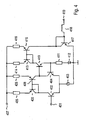
- Figure 4 illustrates an embodiment of a bias voltage circuitry.
- the bias voltage circuitry includes a reference voltage input 401 coupled to a base of a sixth npn-transistor 402.
- An emitter of the sixth npn-transistor 402 is connected to a constant current source 403.
- the emitter of the sixth npn-transistor 402 is also connected to an emitter of a seventh npn-transistor 404.
- a collector of the sixth transistor 402 is connected to a collector and a base of a first pnp-transistor 405.
- the base and the collector of the first pnp-transistor 405 are directly coupled so that the first pnp-transistor 405 is diode-connected.
- An emitter of the first pnp-transistor 405 is connected via a second resistor 406 to a second constant supply voltage input 407.
- the base of the first pnp-transistor 405 is connected to a base of a second pnp-transistor 408.
- An emitter of the second pnp-transistor 408 is connected via a third resistor 409 to the second constant supply voltage input 407.
- a collector of the second pnp-transistor 408 is connected to a collector of the seventh npn-transistor 404.
- the sixth npn-transistor 402 and the seventh npn-transistor 404 form a differential pair, while the first pnp-transistor 405 and the second pnp-transistor 408 are current-mirror-coupled. All these elements are connected as a differential amplifier with an active load.
- the current mirror formed by the first pnp-transistor 405 and the second pnp-transistor 408 may be considered as active load.
- the collector of the seventh npn-transistor 404 and the collector of the second pnp-transistor 408 are both connected to a base of an eighth npn-transistor 410.
- An emitter of the eighth npn-transistor 410 and a base of the seventh npn-transistor 404 are both connected via a fourth resistor 411 and a diode 412 coupled in series to ground.
- a collector of the eighth npn-transistor 410 is connected to a collector and a base of a third pnp-transistor 413.
- An emitter of the third pnp-transistor 413 is connected via a fifth resistor 414 to the constant supply voltage input 407.
- the base and the collector of the third pnp-transistor 413 are directly connected so that the third pnp-transistor 413 is diode-connected.
- the base of the third pnp-transistor 413 is connected to a base of a fourth pnp-transistor 415.
- the emitter of the fourth pnp-transistor 415 is connected via a sixth resistor 416 to the constant supply voltage input 407.
- the third pnp-transistor 413 and the fourth pnp-transistor 415 form a current mirror.
- a collector of the fourth pnp-transistor 415 is connected to a collector and a base of a ninth npn-transistor 417.
- An emitter of the ninth npn-transistor 417 is grounded.
- the collector and the base of the ninth npn-transistor 417 are directly coupled so that the ninth npn-transistor is diode-connected.
- the collector and the base of the ninth npn-transistor 417 are connected via a seventh inductor 418 to a bias voltage output 419.
- the bias voltage circuitry of Figure 4 calculates a bias voltage provided at the bias voltage output 419 from a reference voltage fed into the reference voltage input 401.
- the relation of the bias voltage with respect to the reference voltage is taking into account a temperature dependence of the diode 412.
- the diode 412 is replaced by a diode coupled to the reference voltage input 401 to get a relation between bias voltage and reference voltage that is temperature dependent.
- the diode 412 i.e. an explicit temperature dependence, is completely omitted.
- the reference voltage could be the supply voltage fed into a first amplifier such as the pre-amplifier stage shown in Figure 2 or Figure 3 . It could be any derivative thereof or it could correspond to a supply voltage control signal fed into a supply voltage circuitry.
- the bias voltage provided at the bias voltage output 419 could be fed directly or indirectly via a resistor or an inductor into a second amplifier such as the output stage shown in Figure 2 or Figure 3 . It could as well be fed either directly or indirectly in another amplifier, such as the first amplifier.
Landscapes
- Engineering & Computer Science (AREA)
- Power Engineering (AREA)
- Amplifiers (AREA)
- Control Of Electrical Variables (AREA)
Claims (27)
- Verstärkervorrichtung (106), aufweisend:- einen Verstärker (202, 204, 205);- wobei der Verstärker eine Vorverstärkerstufe (204) und eine Endstufe (205) aufweist, wobei die Vorverstärkerstufe (204) mit der Endstufe (205) seriell gekoppelt ist;- eine Vorspannungsschaltung (208), die mit der Vorverstärkerstufe (204) und der Endstufe (205) gekoppelt ist, um der Vorverstärkerstufe (204) und der Endstufe (205) eine Vorspannung bereitzustellen;- eine Versorgungsspannungsschaltung (207), die mit der Vorverstärkerstufe (204) gekoppelt ist, um ihr eine Versorgungsspannung zu liefern;wobei die Versorgungsspannungsschaltung (207) mit der Vorspannungsschaltung (208) gekoppelt ist, und
wobei die Vorspannungsschaltung (208) dazu ausgestaltet ist, die Biasspannung der Vorverstärkerstufe (204) und der Endstufe (205) in Abhängigkeit von der Versorgungsspannung bereitzustellen. - Verstärkervorrichtung (106) nach Anspruch 1,
wobei der Verstärker (202, 204, 205) ferner eine dritte Verstärkerstufe (202) aufweist, die mit der ersten Verstärkerstufe (204) und der zweiten Verstärkerstufe (205) seriell gekoppelt ist. - Verstärkervorrichtung (106) nach Anspruch 2,
wobei die dritte Verstärkerstufe (202) eine variable Verstärkerstufe (202) ist. - Verstärkervorrichtung (106) nach Anspruch 1,
ferner aufweisend einen Versorgungsspannungssteuersignaleingang (209), der mit der Versorgungsspannungsschaltung (207) gekoppelt ist, um die Versorgungsspannungsschaltung (207) mit einem Versorgungsspannungssteuersignal zu versorgen. - Verstärkervorrichtung (106) nach Anspruch 1,
wobei die Versorgungsspannung von einer allgemeinen Versorgungsspannung in Abhängigkeit von dem Versorgungsspannungssteuersignal abgeleitet ist. - Verstärkervorrichtung (106) nach Anspruch 1,
wobei die Versorgungsspannungsschaltung (207) einen linearen Regler (319) aufweist, um eine von einer konstanten Versorgungsspannung abgeleitete Versorgungsspannung bereitzustellen. - Verstärkervorrichtung (106) nach Anspruch 1,
wobei die Biasspannungsschaltung (208) eine spannungsgesteuerte Stromquelle (401-412) aufweist. - Verstärkervorrichtung (106) nach Anspruch 7,
wobei die spannungsgesteuerte Stromquelle (401-412) dazu ausgestaltet ist, die Versorgungsspannung oder eine Ableitung davon zu empfangen. - Verstärkervorrichtung (106) nach Anspruch 7,
wobei die spannungsgesteuerte Stromquelle (401-412) dazu ausgestaltet ist, ein Versorgungsspannungssteuersignal zu empfangen. - Verstärkervorrichtung (106) nach Anspruch 7,
wobei die spannungsgesteuerte Stromquelle (401-412) eine Rückkopplung durch einen Widerstand (411, 412) aufweist. - Verstärkervorrichtung (106) nach Anspruch 10,
wobei der Widerstand (411, 412) ein temperaturabhängiges Element (412) aufweist. - Verstärkervorrichtung (106) nach Anspruch 11,
wobei das temperaturabhängige Element (412) eine Diode (412) ist. - Verstärkervorrichtung (106) nach Anspruch 1,- wobei die Vorverstärkerstufe (204) dazu ausgestaltet ist, ein Eingangssignal zu empfangen und ein Ausgangssignal bereitzustellen;- wobei die Versorgungsspannungsschaltung (207) einen Leistungsregler (207) aufweist, der an die Vorverstärkerstufe (204) angeschlossen ist, wobei der Leistungsregler (207) dazu ausgestaltet ist, der Vorverstärkerstufe (204) ein Leistungssteuersignal bereitzustellen, um eine Ausgangsleistung des Ausgangssignals zu regeln;- wobei die Endstufe (205) dazu ausgestaltet ist, das Ausgangssignal zu empfangen und ein Übertragungssignal bereitzustellen;- einen Kontroller (208), der an die Vorverstärkerstufe (204) und die Endstufe (205) angeschlossen ist, der ein Betriebssteuersignal der Vorverstärkerstufe (204) und der Endstufe (205) bereitstellt, um deren Arbeitspunkt zu steuern;wobei der Kontroller (208) an den Leistungsregler (207) angeschlossen ist, um das Leistungssteuersignal zu empfangen; und wobei die Vorspannungsschaltung (208) einen Kontroller (208) aufweist, der dazu ausgestaltet ist, das Betriebsteuersignal an die Endstufe (205) als eine Funktion des Leistungssteuersignals zu berechnen.
- Verstärkervorrichtung (106) nach Anspruch 13,
ferner aufweisend einen Spannungsverstärker (202), der dazu ausgestaltet ist, ein Funkfrequenzsignal zu empfangen und das Eingangssignal bereitzustellen. - Verstärkervorrichtung (106) nach Anspruch 14,
wobei der Spannungsverstärker (202) einen Verstärkungseinstelleingang (203) aufweist, um ein Verstärkungseinstellsignal zu empfangen. - Verstärkervorrichtung (106) nach Anspruch 15,
wobei das Verstärkungseinstellsignal eine Amplitudeninformation des Übertragungssignals darstellt. - Verstärkervorrichtung (106) nach Anspruch 15,
wobei das Verstärkungseinstellsignal eine Anstiegsinformation des Übertragungssignals darstellt. - Verstärkervorrichtung (106) nach Anspruch 13,
wobei der Leistungsregler (207) einen Linearregler (319) aufweist, der dazu ausgestaltet ist, ein zweites Verstärkungseinstellsignal zu empfangen. - Verstärkervorrichtung (106) nach Anspruch 15,
wobei das zweite Verstärkungseinstellsignal eine Amplitudeninformation des Übertragungssignals darstellt. - Verstärkervorrichtung (106) nach Anspruch 15,
wobei das zweite Verstärkungseinstellsignal eine Anstiegsinformation des Übertragungssignals darstellt. - Verfahren zum Regeln einer Verstärkervorrichtung (106) nach einem der Ansprüche 1 bis 20, wobei das Verfahren aufweist:- Bereitstellen eines ersten Signals;- Einstellen einer Versorgungsspannung der Vorverstärkerstufe (204) gemäß dem ersten Signal;- Bereitstellen eines zweiten Signals in Abhängigkeit von der Versorgungsspannung;- Einstellen einer Vorspannung des Ausgangsverstärkers (205) in Abhängigkeit von dem zweiten Signal.
- Verfahren für die Leistungsanpassung eines Verstärkers (202, 204, 205) nach einem der Ansprüche 1 bis 20, wobei das Verfahren aufweist:- Bereitstellen eines Leistungssignals;- Einstellen einer Verstärkung der Vorverstärkerstufe (204) gemäß dem Leistungssignal;- Berechnen eines Betriebssteuersignals in Abhängigkeit von dem Leistungssignal;- Einstellen eines Arbeitspunkts der Endstufe (205) in Abhängigkeit von dem Betriebssteuersignal.
- Verfahren nach Anspruch 22, ferner aufweisend:- Einstellen eines zweiten Arbeitspunkts der Vorverstärkerstufe (204) in Abhängigkeit von dem Betriebssteuersignal.
- Verfahren nach Anspruch 22, ferner aufweisend:- Empfangen eines ersten Eingangssignals an einem Eingang der Vorverstärkerstufe (204);- Verstärken des ersten Eingangssignals; und- Zuführen des verstärkten Signals der Endstufe (205), um ein Übertragungssignal bereitzustellen.
- Verfahren nach Anspruch 22,
wobei das Leistungssignal eine Amplitudeninformation des Übertragungssignals aufweist. - Verfahren nach Anspruch 22, ferner aufweisend:- Bereitstellen des ersten Eingangssignals als Ausgangssignal eines Verstärkers (202) mit variabler Verstärkung.
- Verfahren nach Anspruch 26, ferner aufweisend:- Einstellen einer Amplitudeninformation des Übertragungssignals durch Variieren der Verstärkung des Verstärkers (202) mit variabler Verstärkung.
Applications Claiming Priority (1)
| Application Number | Priority Date | Filing Date | Title |
|---|---|---|---|
| US11/479,075 US7456693B2 (en) | 2006-06-30 | 2006-06-30 | Regulation of an amplification apparatus |
Publications (3)
| Publication Number | Publication Date |
|---|---|
| EP1876704A2 EP1876704A2 (de) | 2008-01-09 |
| EP1876704A3 EP1876704A3 (de) | 2008-03-26 |
| EP1876704B1 true EP1876704B1 (de) | 2011-03-16 |
Family
ID=38670038
Family Applications (1)
| Application Number | Title | Priority Date | Filing Date |
|---|---|---|---|
| EP07111332A Not-in-force EP1876704B1 (de) | 2006-06-30 | 2007-06-28 | Regulierung einer Verstärkervorrichtung |
Country Status (4)
| Country | Link |
|---|---|
| US (1) | US7456693B2 (de) |
| EP (1) | EP1876704B1 (de) |
| AT (1) | ATE502437T1 (de) |
| DE (1) | DE602007013144D1 (de) |
Families Citing this family (3)
| Publication number | Priority date | Publication date | Assignee | Title |
|---|---|---|---|---|
| KR101753738B1 (ko) * | 2011-09-22 | 2017-07-07 | 한국전자통신연구원 | 아날로그 디지털 변환기 및 그것의 전력 절감 방법 |
| WO2017062427A1 (en) * | 2015-10-05 | 2017-04-13 | Skyworks Solutions, Inc. | Power amplification system with adaptive bias control |
| IL284937B2 (en) | 2021-07-15 | 2024-06-01 | Elbit Security Systems Ltd | Modular combat system and method |
Family Cites Families (24)
| Publication number | Priority date | Publication date | Assignee | Title |
|---|---|---|---|---|
| US3619798A (en) | 1969-11-20 | 1971-11-09 | Canadian Patents Dev | Three-port electrical network |
| CA2017904C (en) | 1989-05-31 | 1993-11-16 | Shinichi Miyazaki | High frequency amplifier circuit capable of optimizing a total power consumption |
| JP2570878B2 (ja) | 1990-02-01 | 1997-01-16 | 日本電気株式会社 | 高周波電力増幅器 |
| US5276917A (en) | 1991-10-22 | 1994-01-04 | Nokia Mobile Phones Ltd. | Transmitter switch-on in a dual-mode mobile phone |
| US5432473A (en) | 1993-07-14 | 1995-07-11 | Nokia Mobile Phones, Limited | Dual mode amplifier with bias control |
| JP2552089B2 (ja) | 1994-05-23 | 1996-11-06 | 埼玉日本電気株式会社 | Fet増幅器の消費電力低減方式 |
| JP3688413B2 (ja) | 1995-12-21 | 2005-08-31 | 株式会社東芝 | 出力回路 |
| US6148220A (en) | 1997-04-25 | 2000-11-14 | Triquint Semiconductor, Inc. | Battery life extending technique for mobile wireless applications |
| US6031417A (en) | 1998-04-01 | 2000-02-29 | Rockwell International | Differential amplifier for multiple supply voltages and biasing device therefore |
| US6008698A (en) | 1998-05-18 | 1999-12-28 | Omnipoint Corporation | Amplifier with dynamically adaptable supply current |
| US6081161A (en) * | 1998-05-18 | 2000-06-27 | Omnipoint Corporation | Amplifier with dynamatically adaptable supply voltage |
| JP2001284998A (ja) | 2000-03-31 | 2001-10-12 | Mitsubishi Electric Corp | 無線送信装置 |
| US6617928B2 (en) * | 2000-10-06 | 2003-09-09 | Skyworks Solutions, Inc. | Configurable power amplifier and bias control |
| US6323731B1 (en) | 2000-10-06 | 2001-11-27 | Tropion, Inc. Corp. | Variable bias control for switch mode RF amplifier |
| JP3844429B2 (ja) * | 2000-12-12 | 2006-11-15 | 富士通テン株式会社 | 走査型レーダ装置 |
| US6701138B2 (en) | 2001-06-11 | 2004-03-02 | Rf Micro Devices, Inc. | Power amplifier control |
| US20050087308A1 (en) * | 2002-07-24 | 2005-04-28 | Vaughan David M. | Office cubicle door |
| US20040169530A1 (en) | 2002-09-27 | 2004-09-02 | Engim, Inc. | Method and apparatus for robust biasing of bipolar and BiCMOS differential architectures |
| JP2004274433A (ja) | 2003-03-10 | 2004-09-30 | Mitsubishi Electric Corp | 高周波集積回路装置 |
| EP1658671A1 (de) | 2003-06-16 | 2006-05-24 | Paragon Communications Ltd. | Verfahren und vorrichtung zur dynamischen regelung der versorgungsspannung eines leistungsverstärkers |
| EP1499016B1 (de) | 2003-07-17 | 2009-05-13 | Palm, Inc. | Schaltungsanordnung und Verfahren zur Erhöhung des Wirkungsgrades eines Leistungsverstärkers |
| US6903608B2 (en) | 2003-10-30 | 2005-06-07 | Sige Semiconductor Inc. | Power level controlling of first amplification stage for an integrated RF power amplifier |
| US7193459B1 (en) * | 2004-06-23 | 2007-03-20 | Rf Micro Devices, Inc. | Power amplifier control technique for enhanced efficiency |
| US7248845B2 (en) | 2004-07-09 | 2007-07-24 | Kyocera Wireless Corp. | Variable-loss transmitter and method of operation |
-
2006
- 2006-06-30 US US11/479,075 patent/US7456693B2/en active Active
-
2007
- 2007-06-28 DE DE602007013144T patent/DE602007013144D1/de active Active
- 2007-06-28 AT AT07111332T patent/ATE502437T1/de not_active IP Right Cessation
- 2007-06-28 EP EP07111332A patent/EP1876704B1/de not_active Not-in-force
Also Published As
| Publication number | Publication date |
|---|---|
| DE602007013144D1 (de) | 2011-04-28 |
| US20080001674A1 (en) | 2008-01-03 |
| US7456693B2 (en) | 2008-11-25 |
| EP1876704A3 (de) | 2008-03-26 |
| ATE502437T1 (de) | 2011-04-15 |
| EP1876704A2 (de) | 2008-01-09 |
Similar Documents
| Publication | Publication Date | Title |
|---|---|---|
| EP1776753B1 (de) | System und verfahren für strommodus-amplitudenmodulation | |
| KR101793733B1 (ko) | 송신기에서 전원변조 교정을 위한 장치 및 방법 | |
| EP1410494B1 (de) | System zur strommodus-amplitudenmodulation , und verfahren dazu | |
| KR100757371B1 (ko) | 고주파 신호의 엔벨롭 변조를 위한 전력 증폭기 회로 및방법 | |
| US7639080B2 (en) | Radio frequency amplifier circuit and mobile communication terminal using the same | |
| US11165392B2 (en) | Variable power amplifier bias impedance | |
| KR101746107B1 (ko) | 적응형 전력증폭기 및 이를 포함하는 rf 송신기 | |
| US20040201418A1 (en) | Power supply processing for power amplifiers | |
| US7315211B1 (en) | Sliding bias controller for use with radio frequency power amplifiers | |
| WO2002101944A2 (en) | Power amplifier control | |
| WO2004027983A2 (en) | Saturated power amplifier with selectable and variable output power levels | |
| US8525595B2 (en) | Vramp limiting using resistors | |
| US8791760B2 (en) | Closed loop bias control | |
| US7616055B2 (en) | Transmitter apparatus with extended gain control | |
| JP2006094076A (ja) | 高周波電力増幅回路および高周波電力増幅用電子部品 | |
| US7027783B2 (en) | Method and apparatus providing reduction in transmitter current consumption using signal derived from rectified input signal | |
| KR20080010569A (ko) | 고주파 신호의 피크 엔벨롭 변조를 위한 전력 증폭기 회로 | |
| EP1876704A2 (de) | Regulierung einer Verstärkervorrichtung | |
| US7782133B2 (en) | Power amplifier with output power control | |
| CN1123114C (zh) | 具有用于通信的多个便携装置的无线通信系统 | |
| US20030169112A1 (en) | Variable gain amplifier with low power consumption | |
| JP2006303850A (ja) | 高周波電力増幅回路および無線通信端末 | |
| JP2005143048A (ja) | 高周波電力増幅器モジュール | |
| KR20060114926A (ko) | 전력증폭모듈 |
Legal Events
| Date | Code | Title | Description |
|---|---|---|---|
| PUAI | Public reference made under article 153(3) epc to a published international application that has entered the european phase |
Free format text: ORIGINAL CODE: 0009012 |
|
| AK | Designated contracting states |
Kind code of ref document: A2 Designated state(s): AT BE BG CH CY CZ DE DK EE ES FI FR GB GR HU IE IS IT LI LT LU LV MC MT NL PL PT RO SE SI SK TR |
|
| AX | Request for extension of the european patent |
Extension state: AL BA HR MK YU |
|
| PUAL | Search report despatched |
Free format text: ORIGINAL CODE: 0009013 |
|
| AK | Designated contracting states |
Kind code of ref document: A3 Designated state(s): AT BE BG CH CY CZ DE DK EE ES FI FR GB GR HU IE IS IT LI LT LU LV MC MT NL PL PT RO SE SI SK TR |
|
| AX | Request for extension of the european patent |
Extension state: AL BA HR MK YU |
|
| 17P | Request for examination filed |
Effective date: 20080424 |
|
| 17Q | First examination report despatched |
Effective date: 20080523 |
|
| AKX | Designation fees paid |
Designated state(s): AT BE BG CH CY CZ DE DK EE ES FI FR GB GR HU IE IS IT LI LT LU LV MC MT NL PL PT RO SE SI SK TR |
|
| RAP1 | Party data changed (applicant data changed or rights of an application transferred) |
Owner name: INFINEON TECHNOLOGIES AG |
|
| GRAJ | Information related to disapproval of communication of intention to grant by the applicant or resumption of examination proceedings by the epo deleted |
Free format text: ORIGINAL CODE: EPIDOSDIGR1 |
|
| GRAP | Despatch of communication of intention to grant a patent |
Free format text: ORIGINAL CODE: EPIDOSNIGR1 |
|
| GRAS | Grant fee paid |
Free format text: ORIGINAL CODE: EPIDOSNIGR3 |
|
| GRAA | (expected) grant |
Free format text: ORIGINAL CODE: 0009210 |
|
| AK | Designated contracting states |
Kind code of ref document: B1 Designated state(s): AT BE BG CH CY CZ DE DK EE ES FI FR GB GR HU IE IS IT LI LT LU LV MC MT NL PL PT RO SE SI SK TR |
|
| REG | Reference to a national code |
Ref country code: GB Ref legal event code: FG4D |
|
| REG | Reference to a national code |
Ref country code: CH Ref legal event code: EP |
|
| REG | Reference to a national code |
Ref country code: IE Ref legal event code: FG4D |
|
| REF | Corresponds to: |
Ref document number: 602007013144 Country of ref document: DE Date of ref document: 20110428 Kind code of ref document: P |
|
| REG | Reference to a national code |
Ref country code: DE Ref legal event code: R096 Ref document number: 602007013144 Country of ref document: DE Effective date: 20110428 |
|
| REG | Reference to a national code |
Ref country code: NL Ref legal event code: VDEP Effective date: 20110316 |
|
| PG25 | Lapsed in a contracting state [announced via postgrant information from national office to epo] |
Ref country code: ES Free format text: LAPSE BECAUSE OF FAILURE TO SUBMIT A TRANSLATION OF THE DESCRIPTION OR TO PAY THE FEE WITHIN THE PRESCRIBED TIME-LIMIT Effective date: 20110627 Ref country code: SE Free format text: LAPSE BECAUSE OF FAILURE TO SUBMIT A TRANSLATION OF THE DESCRIPTION OR TO PAY THE FEE WITHIN THE PRESCRIBED TIME-LIMIT Effective date: 20110316 Ref country code: LV Free format text: LAPSE BECAUSE OF FAILURE TO SUBMIT A TRANSLATION OF THE DESCRIPTION OR TO PAY THE FEE WITHIN THE PRESCRIBED TIME-LIMIT Effective date: 20110316 Ref country code: GR Free format text: LAPSE BECAUSE OF FAILURE TO SUBMIT A TRANSLATION OF THE DESCRIPTION OR TO PAY THE FEE WITHIN THE PRESCRIBED TIME-LIMIT Effective date: 20110617 Ref country code: LT Free format text: LAPSE BECAUSE OF FAILURE TO SUBMIT A TRANSLATION OF THE DESCRIPTION OR TO PAY THE FEE WITHIN THE PRESCRIBED TIME-LIMIT Effective date: 20110316 |
|
| LTIE | Lt: invalidation of european patent or patent extension |
Effective date: 20110316 |
|
| PG25 | Lapsed in a contracting state [announced via postgrant information from national office to epo] |
Ref country code: AT Free format text: LAPSE BECAUSE OF FAILURE TO SUBMIT A TRANSLATION OF THE DESCRIPTION OR TO PAY THE FEE WITHIN THE PRESCRIBED TIME-LIMIT Effective date: 20110316 Ref country code: CY Free format text: LAPSE BECAUSE OF FAILURE TO SUBMIT A TRANSLATION OF THE DESCRIPTION OR TO PAY THE FEE WITHIN THE PRESCRIBED TIME-LIMIT Effective date: 20110316 Ref country code: BG Free format text: LAPSE BECAUSE OF FAILURE TO SUBMIT A TRANSLATION OF THE DESCRIPTION OR TO PAY THE FEE WITHIN THE PRESCRIBED TIME-LIMIT Effective date: 20110616 Ref country code: SI Free format text: LAPSE BECAUSE OF FAILURE TO SUBMIT A TRANSLATION OF THE DESCRIPTION OR TO PAY THE FEE WITHIN THE PRESCRIBED TIME-LIMIT Effective date: 20110316 Ref country code: FI Free format text: LAPSE BECAUSE OF FAILURE TO SUBMIT A TRANSLATION OF THE DESCRIPTION OR TO PAY THE FEE WITHIN THE PRESCRIBED TIME-LIMIT Effective date: 20110316 |
|
| PG25 | Lapsed in a contracting state [announced via postgrant information from national office to epo] |
Ref country code: BE Free format text: LAPSE BECAUSE OF FAILURE TO SUBMIT A TRANSLATION OF THE DESCRIPTION OR TO PAY THE FEE WITHIN THE PRESCRIBED TIME-LIMIT Effective date: 20110316 |
|
| PG25 | Lapsed in a contracting state [announced via postgrant information from national office to epo] |
Ref country code: PT Free format text: LAPSE BECAUSE OF FAILURE TO SUBMIT A TRANSLATION OF THE DESCRIPTION OR TO PAY THE FEE WITHIN THE PRESCRIBED TIME-LIMIT Effective date: 20110718 Ref country code: EE Free format text: LAPSE BECAUSE OF FAILURE TO SUBMIT A TRANSLATION OF THE DESCRIPTION OR TO PAY THE FEE WITHIN THE PRESCRIBED TIME-LIMIT Effective date: 20110316 |
|
| PG25 | Lapsed in a contracting state [announced via postgrant information from national office to epo] |
Ref country code: IS Free format text: LAPSE BECAUSE OF FAILURE TO SUBMIT A TRANSLATION OF THE DESCRIPTION OR TO PAY THE FEE WITHIN THE PRESCRIBED TIME-LIMIT Effective date: 20110716 Ref country code: SK Free format text: LAPSE BECAUSE OF FAILURE TO SUBMIT A TRANSLATION OF THE DESCRIPTION OR TO PAY THE FEE WITHIN THE PRESCRIBED TIME-LIMIT Effective date: 20110316 Ref country code: RO Free format text: LAPSE BECAUSE OF FAILURE TO SUBMIT A TRANSLATION OF THE DESCRIPTION OR TO PAY THE FEE WITHIN THE PRESCRIBED TIME-LIMIT Effective date: 20110316 Ref country code: CZ Free format text: LAPSE BECAUSE OF FAILURE TO SUBMIT A TRANSLATION OF THE DESCRIPTION OR TO PAY THE FEE WITHIN THE PRESCRIBED TIME-LIMIT Effective date: 20110316 |
|
| PG25 | Lapsed in a contracting state [announced via postgrant information from national office to epo] |
Ref country code: MT Free format text: LAPSE BECAUSE OF FAILURE TO SUBMIT A TRANSLATION OF THE DESCRIPTION OR TO PAY THE FEE WITHIN THE PRESCRIBED TIME-LIMIT Effective date: 20110316 Ref country code: NL Free format text: LAPSE BECAUSE OF FAILURE TO SUBMIT A TRANSLATION OF THE DESCRIPTION OR TO PAY THE FEE WITHIN THE PRESCRIBED TIME-LIMIT Effective date: 20110316 |
|
| PLBE | No opposition filed within time limit |
Free format text: ORIGINAL CODE: 0009261 |
|
| STAA | Information on the status of an ep patent application or granted ep patent |
Free format text: STATUS: NO OPPOSITION FILED WITHIN TIME LIMIT |
|
| REG | Reference to a national code |
Ref country code: CH Ref legal event code: PL |
|
| 26N | No opposition filed |
Effective date: 20111219 |
|
| GBPC | Gb: european patent ceased through non-payment of renewal fee |
Effective date: 20110628 |
|
| PG25 | Lapsed in a contracting state [announced via postgrant information from national office to epo] |
Ref country code: DK Free format text: LAPSE BECAUSE OF FAILURE TO SUBMIT A TRANSLATION OF THE DESCRIPTION OR TO PAY THE FEE WITHIN THE PRESCRIBED TIME-LIMIT Effective date: 20110316 Ref country code: PL Free format text: LAPSE BECAUSE OF FAILURE TO SUBMIT A TRANSLATION OF THE DESCRIPTION OR TO PAY THE FEE WITHIN THE PRESCRIBED TIME-LIMIT Effective date: 20110316 |
|
| REG | Reference to a national code |
Ref country code: FR Ref legal event code: ST Effective date: 20120229 |
|
| REG | Reference to a national code |
Ref country code: IE Ref legal event code: MM4A |
|
| REG | Reference to a national code |
Ref country code: DE Ref legal event code: R097 Ref document number: 602007013144 Country of ref document: DE Effective date: 20111219 |
|
| PG25 | Lapsed in a contracting state [announced via postgrant information from national office to epo] |
Ref country code: IE Free format text: LAPSE BECAUSE OF NON-PAYMENT OF DUE FEES Effective date: 20110628 Ref country code: FR Free format text: LAPSE BECAUSE OF NON-PAYMENT OF DUE FEES Effective date: 20110630 Ref country code: LI Free format text: LAPSE BECAUSE OF NON-PAYMENT OF DUE FEES Effective date: 20110630 Ref country code: CH Free format text: LAPSE BECAUSE OF NON-PAYMENT OF DUE FEES Effective date: 20110630 |
|
| PG25 | Lapsed in a contracting state [announced via postgrant information from national office to epo] |
Ref country code: IT Free format text: LAPSE BECAUSE OF FAILURE TO SUBMIT A TRANSLATION OF THE DESCRIPTION OR TO PAY THE FEE WITHIN THE PRESCRIBED TIME-LIMIT Effective date: 20110316 |
|
| PG25 | Lapsed in a contracting state [announced via postgrant information from national office to epo] |
Ref country code: GB Free format text: LAPSE BECAUSE OF NON-PAYMENT OF DUE FEES Effective date: 20110628 |
|
| PG25 | Lapsed in a contracting state [announced via postgrant information from national office to epo] |
Ref country code: MC Free format text: LAPSE BECAUSE OF NON-PAYMENT OF DUE FEES Effective date: 20110630 |
|
| PG25 | Lapsed in a contracting state [announced via postgrant information from national office to epo] |
Ref country code: LU Free format text: LAPSE BECAUSE OF NON-PAYMENT OF DUE FEES Effective date: 20110628 |
|
| PG25 | Lapsed in a contracting state [announced via postgrant information from national office to epo] |
Ref country code: TR Free format text: LAPSE BECAUSE OF FAILURE TO SUBMIT A TRANSLATION OF THE DESCRIPTION OR TO PAY THE FEE WITHIN THE PRESCRIBED TIME-LIMIT Effective date: 20110316 |
|
| PG25 | Lapsed in a contracting state [announced via postgrant information from national office to epo] |
Ref country code: HU Free format text: LAPSE BECAUSE OF FAILURE TO SUBMIT A TRANSLATION OF THE DESCRIPTION OR TO PAY THE FEE WITHIN THE PRESCRIBED TIME-LIMIT Effective date: 20110316 |
|
| REG | Reference to a national code |
Ref country code: DE Ref legal event code: R081 Ref document number: 602007013144 Country of ref document: DE Owner name: INTEL DEUTSCHLAND GMBH, DE Free format text: FORMER OWNER: INFINEON TECHNOLOGIES AG, 85579 NEUBIBERG, DE Ref country code: DE Ref legal event code: R081 Ref document number: 602007013144 Country of ref document: DE Owner name: APPLE INC., CUPERTINO, US Free format text: FORMER OWNER: INFINEON TECHNOLOGIES AG, 85579 NEUBIBERG, DE Ref country code: DE Ref legal event code: R081 Ref document number: 602007013144 Country of ref document: DE Owner name: INTEL MOBILE COMMUNICATIONS GMBH, DE Free format text: FORMER OWNER: INFINEON TECHNOLOGIES AG, 85579 NEUBIBERG, DE |
|
| REG | Reference to a national code |
Ref country code: DE Ref legal event code: R081 Ref document number: 602007013144 Country of ref document: DE Owner name: INTEL DEUTSCHLAND GMBH, DE Free format text: FORMER OWNER: INTEL MOBILE COMMUNICATIONS GMBH, 85579 NEUBIBERG, DE Ref country code: DE Ref legal event code: R081 Ref document number: 602007013144 Country of ref document: DE Owner name: APPLE INC., CUPERTINO, US Free format text: FORMER OWNER: INTEL MOBILE COMMUNICATIONS GMBH, 85579 NEUBIBERG, DE |
|
| REG | Reference to a national code |
Ref country code: DE Ref legal event code: R081 Ref document number: 602007013144 Country of ref document: DE Owner name: APPLE INC., CUPERTINO, US Free format text: FORMER OWNER: INTEL DEUTSCHLAND GMBH, 80336 MUENCHEN, DE |
|
| PGFP | Annual fee paid to national office [announced via postgrant information from national office to epo] |
Ref country code: DE Payment date: 20210602 Year of fee payment: 15 |
|
| REG | Reference to a national code |
Ref country code: DE Ref legal event code: R119 Ref document number: 602007013144 Country of ref document: DE |
|
| PG25 | Lapsed in a contracting state [announced via postgrant information from national office to epo] |
Ref country code: DE Free format text: LAPSE BECAUSE OF NON-PAYMENT OF DUE FEES Effective date: 20230103 |