EP1878694A2 - Verfahren zur Nanostrukturierung der Oberfläche eines Substrats - Google Patents
Verfahren zur Nanostrukturierung der Oberfläche eines Substrats Download PDFInfo
- Publication number
- EP1878694A2 EP1878694A2 EP07112226A EP07112226A EP1878694A2 EP 1878694 A2 EP1878694 A2 EP 1878694A2 EP 07112226 A EP07112226 A EP 07112226A EP 07112226 A EP07112226 A EP 07112226A EP 1878694 A2 EP1878694 A2 EP 1878694A2
- Authority
- EP
- European Patent Office
- Prior art keywords
- substrate
- implants
- process according
- crystalline
- thermally
- Prior art date
- Legal status (The legal status is an assumption and is not a legal conclusion. Google has not performed a legal analysis and makes no representation as to the accuracy of the status listed.)
- Withdrawn
Links
Images



Classifications
-
- B—PERFORMING OPERATIONS; TRANSPORTING
- B81—MICROSTRUCTURAL TECHNOLOGY
- B81C—PROCESSES OR APPARATUS SPECIALLY ADAPTED FOR THE MANUFACTURE OR TREATMENT OF MICROSTRUCTURAL DEVICES OR SYSTEMS
- B81C1/00—Manufacture or treatment of devices or systems in or on a substrate
- B81C1/00436—Shaping materials, i.e. techniques for structuring the substrate or the layers on the substrate
- B81C1/00634—Processes for shaping materials not provided for in groups B81C1/00444 - B81C1/00626
-
- H—ELECTRICITY
- H10—SEMICONDUCTOR DEVICES; ELECTRIC SOLID-STATE DEVICES NOT OTHERWISE PROVIDED FOR
- H10P—GENERIC PROCESSES OR APPARATUS FOR THE MANUFACTURE OR TREATMENT OF DEVICES COVERED BY CLASS H10
- H10P30/00—Ion implantation into wafers, substrates or parts of devices
- H10P30/20—Ion implantation into wafers, substrates or parts of devices into semiconductor materials, e.g. for doping
- H10P30/202—Ion implantation into wafers, substrates or parts of devices into semiconductor materials, e.g. for doping characterised by the semiconductor materials
- H10P30/204—Ion implantation into wafers, substrates or parts of devices into semiconductor materials, e.g. for doping characterised by the semiconductor materials into Group IV semiconductors
-
- H—ELECTRICITY
- H10—SEMICONDUCTOR DEVICES; ELECTRIC SOLID-STATE DEVICES NOT OTHERWISE PROVIDED FOR
- H10P—GENERIC PROCESSES OR APPARATUS FOR THE MANUFACTURE OR TREATMENT OF DEVICES COVERED BY CLASS H10
- H10P30/00—Ion implantation into wafers, substrates or parts of devices
- H10P30/20—Ion implantation into wafers, substrates or parts of devices into semiconductor materials, e.g. for doping
- H10P30/202—Ion implantation into wafers, substrates or parts of devices into semiconductor materials, e.g. for doping characterised by the semiconductor materials
- H10P30/206—Ion implantation into wafers, substrates or parts of devices into semiconductor materials, e.g. for doping characterised by the semiconductor materials into Group III-V semiconductors
-
- H—ELECTRICITY
- H10—SEMICONDUCTOR DEVICES; ELECTRIC SOLID-STATE DEVICES NOT OTHERWISE PROVIDED FOR
- H10P—GENERIC PROCESSES OR APPARATUS FOR THE MANUFACTURE OR TREATMENT OF DEVICES COVERED BY CLASS H10
- H10P30/00—Ion implantation into wafers, substrates or parts of devices
- H10P30/20—Ion implantation into wafers, substrates or parts of devices into semiconductor materials, e.g. for doping
- H10P30/208—Ion implantation into wafers, substrates or parts of devices into semiconductor materials, e.g. for doping of electrically inactive species
-
- H—ELECTRICITY
- H10—SEMICONDUCTOR DEVICES; ELECTRIC SOLID-STATE DEVICES NOT OTHERWISE PROVIDED FOR
- H10P—GENERIC PROCESSES OR APPARATUS FOR THE MANUFACTURE OR TREATMENT OF DEVICES COVERED BY CLASS H10
- H10P32/00—Diffusion of dopants within, into or out of wafers, substrates or parts of devices
- H10P32/10—Diffusion of dopants within, into or out of semiconductor bodies or layers
- H10P32/17—Diffusion of dopants within, into or out of semiconductor bodies or layers characterised by the semiconductor material
- H10P32/171—Diffusion of dopants within, into or out of semiconductor bodies or layers characterised by the semiconductor material being group IV material
-
- H—ELECTRICITY
- H10—SEMICONDUCTOR DEVICES; ELECTRIC SOLID-STATE DEVICES NOT OTHERWISE PROVIDED FOR
- H10P—GENERIC PROCESSES OR APPARATUS FOR THE MANUFACTURE OR TREATMENT OF DEVICES COVERED BY CLASS H10
- H10P32/00—Diffusion of dopants within, into or out of wafers, substrates or parts of devices
- H10P32/10—Diffusion of dopants within, into or out of semiconductor bodies or layers
- H10P32/18—Diffusion lifetime killers
-
- H—ELECTRICITY
- H10—SEMICONDUCTOR DEVICES; ELECTRIC SOLID-STATE DEVICES NOT OTHERWISE PROVIDED FOR
- H10P—GENERIC PROCESSES OR APPARATUS FOR THE MANUFACTURE OR TREATMENT OF DEVICES COVERED BY CLASS H10
- H10P34/00—Irradiation with electromagnetic or particle radiation of wafers, substrates or parts of devices
- H10P34/40—Irradiation with electromagnetic or particle radiation of wafers, substrates or parts of devices with high-energy radiation
- H10P34/42—Irradiation with electromagnetic or particle radiation of wafers, substrates or parts of devices with high-energy radiation with electromagnetic radiation, e.g. laser annealing
-
- B—PERFORMING OPERATIONS; TRANSPORTING
- B81—MICROSTRUCTURAL TECHNOLOGY
- B81B—MICROSTRUCTURAL DEVICES OR SYSTEMS, e.g. MICROMECHANICAL DEVICES
- B81B2203/00—Basic microelectromechanical structures
- B81B2203/03—Static structures
- B81B2203/0323—Grooves
- B81B2203/033—Trenches
-
- B—PERFORMING OPERATIONS; TRANSPORTING
- B81—MICROSTRUCTURAL TECHNOLOGY
- B81C—PROCESSES OR APPARATUS SPECIALLY ADAPTED FOR THE MANUFACTURE OR TREATMENT OF MICROSTRUCTURAL DEVICES OR SYSTEMS
- B81C2201/00—Manufacture or treatment of microstructural devices or systems
- B81C2201/01—Manufacture or treatment of microstructural devices or systems in or on a substrate
- B81C2201/0101—Shaping material; Structuring the bulk substrate or layers on the substrate; Film patterning
- B81C2201/0147—Film patterning
- B81C2201/0154—Film patterning other processes for film patterning not provided for in B81C2201/0149 - B81C2201/015
Definitions
- the present invention relates to a method for nanostructuring the surface of a substrate.
- Many applications in nanotechnology use nanostructures organized for example in microelectronics, optoelectronics or biology. These nanostructures are generally obtained by growth or by deposition on the surface of a substrate. It seeks to control as accurately as possible the density and the period of these nanostructures distributed on the surface of the substrate.
- this nanostructuring can be a pre-engraving as described in the article Controlled arrangement of self-organized Si (001) substrates G. Lin et al. Applied Physics Letters, vol.75, No. 18, pages 2752 to 2754 or for example in the article "Templated Self-Assembly of Block Copolymers: Effect of Substrate Topography” Joy Y. Cheng et al. Advanced Materials 2003, 15, No. 19, October 2, pages 1599-1602 .
- periodic surface nanostructuring it is meant that periodic patterns are produced at the nanoscale at the surface of the host substrate.
- Performing a pre-etching of the host substrate is a simple way of controlling the spatial ordering of the nanostructures during the growth or deposition step.
- This pre-engraving leads to a topographic nanostructuring of the starting substrate, that is to say an embodiment of periodic patterns in relief.
- the bonding is done so as to obtain covalent bonds between the two crystal lattices of the faces to be assembled.
- An arrangement is obtained provided with a grain boundary at the bonding interface and this grain boundary thus causes the appearance of a network of dislocations whose characteristics: orientation, period, type of dislocations, symmetry, depend only on characteristics of the crystalline meshes of the substrate and of the film as well as the angles of disorientation in torsion and bending introduced during bonding. For example, starting from a film and a silicon substrate whose faces to be assembled are oriented in the ⁇ 001> direction, without disorientation of bending and with a twist disorientation of 0.88 °, a network is obtained.
- the object of the present invention is precisely to propose a method of periodic nanostructuring of the surface of a substrate which does not have the disadvantages mentioned above. More precisely, the method of the invention makes it possible to obtain, with great precision, a periodic network of structural patterns on the surface of the substrate. This network is easily produced over large areas and the surface of the nucleation sites is as smooth as possible, which is favorable for the growth or deposition of nanostructures on the patterns.
- Periodic nanostructuring is topographic or thermal.
- irradiating the substrate briefly so as to limit the thermal effects it is possible to ablate at least a portion of the implants resulting in an exfoliation of at least the crystalline material of the crystalline zone in front of the implants, between the implants and the face of the substrate, this ablation and exfoliation helping to form the nanostructuration.
- brief irradiation is in the order of one or more femtoseconds.
- irradiating the substrate more prolonged can cause an increase in temperature of the face by thermal effects.
- This temperature increase can be inhomogeneous at the level of the implants and at the level of the crystalline zone situated between the implants.
- irradiation more prolonged means of the order of one or a few picoseconds or even of the order of one or a few nanoseconds.
- the inhomogeneous increase in temperature can cause plastic deformation or exfoliation of the crystalline material facing the implants, between the implants and the face of the substrate, the deformation or exfoliation contributing to form the nanostructuration.
- the increase in temperature can cause the appearance, on the face of the substrate, of zones more affected thermally compared to the implants, these zones being warmer, these zones more affected thermally bordering zones less affected thermally, that is to say say less warm, these areas more affected thermally and less affected thermally can form the nanostructuration.
- a preferential deposit can be made on the areas more affected thermally vis-à-vis areas less affected thermally, so that the nanostructuration is topographic.
- a deposition based on a phase change material can be made on the face of the substrate before the irradiation, this material this material leading to the nanostructuration.
- the implants can be obtained by thermally diffusing a previously deposited metal material onto one of the faces of the substrate.
- the method consists of removing the remaining metallic material on the deposited surface before irradiation with the electromagnetic wave.
- the metallic material of the implants can be made of gold, titanium, aluminum, platinum, copper, tungsten, nickel, silver.
- the implanted species can be chosen from among gold, titanium, aluminum, copper, platinum, tungsten, nickel, silver or a dopant of the crystalline material.
- a step of homogeneous heating of the substrate before and / or during irradiation, deposition or etching can be carried out to promote the migration of the species and to promote etching.
- the exfoliation can cause a deposition of exfoliated material on the face of the substrate, it is possible to then provide a step of removing the exfoliated material by brushing, chemical cleaning or megasonic.
- the crystalline material of the elements may be selected from silicon, III-V materials such as gallium arsenide, indium arsenide or aluminum nitride, II-VI materials such as cadmium tellurium or aluminum oxide. zinc selenide, or germanium, gallium nitride, silicon germanium Si x Ge y , silicon carbide, indium phosphide, sapphire, quartz, garnet, diamond.
- One of the elements is preferably a film which is on the side of the nanostructured substrate, which allows the dislocations to be close to one of the faces of the substrate.
- the electromagnetic wave can be pulsed or continuous.
- the electromagnetic wave may be monochromatic or almost monochromatic or have one or more wavelengths. When it has several wavelengths, these can be transmitted at the same time or successively, the electromagnetic wave then being subdivided into several parts corresponding to the different wavelengths, these parts having equal or different intensities.
- the method of periodic nanostructuring can be carried out under a controlled atmosphere or in a liquid so as to control the exfoliation and / or facilitate the structuring.
- the present invention also relates to a process for producing nanostructures which comprises a step of depositing a material on a substrate provided with a nanostructuration obtained by the method thus characterized.
- the deposition of the nanostructures can be done for example by molecular jet, taking advantage of a different growth rate between the said zones.
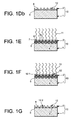
- FIGS. 1A to 1G reference will now be made to an example of a method according to the invention.
- This substrate 10 can be obtained for example as described in the patent application FR-A-2,766,620 .
- the starting substrate 10 is illustrated in FIG. 1A.
- One of the elements 2 may be thinner than the other, it may be preferably a crystalline thin film having for example a thickness less than about 10 micrometers. It is possible that at the time of gluing, the thin film is not available but that it is obtained later by thinning the corresponding element.
- This element can in particular be a composite substrate formed of a stack of a support, a stop layer to thinning, a crystalline thin film. It may be in particular an SOI (semiconductor on insulator or semiconductor on insulator) substrate. It can be provided as in the patent application FR-A-2,819,099 that the thin film has previously been taken from a crystalline base substrate, which remains of the base substrate after the sample has been taken to give the other element. The sampling can be done by producing a buried embrittled zone obtained for example by ion implantation (for example hydrogen), in the base substrate and then fracture at the weakened zone.
- ion implantation for example hydrogen
- the implants 6 will be distributed in the substrate 10 at each dislocation 3 in a material different from that of the crystalline zone 4. in which are the dislocations 3 ( Figure 1B).
- the electromagnetic wave may be delivered by a laser (not shown). It can be continuous or preferably in pulses.
- the pulses may be brief, very advantageously of the order of one or a few femtoseconds or temporally more spread out, of the order of one or a few picoseconds or one or a few nanoseconds. In continuous, we find the same mechanisms as slow pulsed.
- the electromagnetic wave used for the irradiation can be monochromatic or almost monochromatic or on the contrary have several wavelengths.
- these wavelengths can be emitted successively or simultaneously.
- the electromagnetic wave used for the irradiation has several wavelengths, it is subdivided into several parts according to the different wavelengths, these parts having equal or different intensities.
- the implants 6 are atomized and therefore disappear, however it is possible that only a part of the implant disappears causing Exfoliation of what is on it and leave intact what is on it, including some of the implant.
- This removal can be done by conventional techniques in microelectronics such as brushing, chemical cleaning and / or megasonic.
- a step of depositing a sacrificial layer 30 on the substrate 10, on the side of its face which will be irradiated but before irradiation ( Figure 3A). After the irradiation, the exfoliated material 20 will fall on the sacrificial layer 30.
- a detachment step (known by the English name of lift-off), the sacrificial layer 30 and the exfoliated material 20 can be removed. deposited on it.
- the material of the sacrificial layer 30 may for example be silicon oxide.
- the localized absorption of the electromagnetic wave by the implants 6 creates an increase in temperature at the level of the implants 6.
- Localized temperature increase is schematically illustrated in Figure 1E by concentric circles.
- the surface nanostructuring 12 can be caused by the expansion of the material of the implants 6 and / or the material of the crystalline zone 4 which surrounds the implants 6 and consequently by the deformation of the material overlying the implants 6.
- the nanostructuration 12 is then a topographic nanostructuring. Projections 12.1 are formed in front of the implants 6.
- the deformation occurs first, on the face of the substrate closest to the implants, in the example described on the thin film side 2 because its thickness allows the propagation of this deformation.
- This configuration is illustrated in Figure 1F.
- the deformation can in particular be plastic, that is to say permanent or irreversible, it remains after stopping the irradiation with the electromagnetic wave 11.
- the deformation may even lead to exfoliation of the material overlying the implants 6 as shown in FIG. 1G.
- Holes 12.2 are then formed in front of the implants 6.
- the increase in temperature is inhomogeneous at the level of the implants 6 and at the level of the crystalline zone 4 between the implants. More thermally affected areas 7 (i.e., warmer areas) are created adjacent to less thermally affected areas 8 (i.e., less hot areas).
- a deposition step may be by molecular jet, the surface temperature of the host substrate 10 influences the manner in which the atoms of the deposited crystalline material are distributed.
- the deposition is done with different growth rates depending on the temperature of the receiving zone. With this deposit, we obtain a growth of nanostructures 14 as shown in Figure 3E. If a material is deposited on the surface of a substrate having topographic nanostructuring, depending on the affinity between this material and the material on the surface of the substrate, the material will naturally be localized in the hollows if there is a great deal of Affinity and on bumps, if there is little affinity, affine to minimize the energy of the system.
- This material may be a phase change material depending on the temperature such as GeSbTe (germanium antimony tellurium).
- a juxtaposition of amorphous zones 13.1 and crystalline zones 13.2 will be obtained as shown in FIG. 3D.
- the location of the amorphous zones depends in fact on the thermal history of the location, the initial state of the phase-change material. In general, amorphous material is obtained when the cooling after the rise in temperature is rapid and the crystalline material when the cooling is slow.
- phase-change material in crystalline form, to raise locally at the level of the implants 6 the temperature to a temperature sufficient to ensure the transition and to fall rapidly in temperature so as to obtain at the level of the implants amorphous areas.
- Other configurations are of course possible.
- the substrate 10 Before and / or during the growth, deposition, etching or irradiation, it is possible to heat the substrate 10 in a homogeneous manner. This can be done in an oven, the temperature increase can be for example between about 100 ° C and 600 ° C. This increase in temperature takes place globally. The local temperature gradients generated by the irradiation are added to the temperature obtained by the homogeneous heating. This step is not representable. This step makes it possible, for example, in the case of the phase-change material, to locate before irradiation in the vicinity of the transition temperature of the material. It also helps to promote the attack.
- the crystalline material of these two elements may be the same for example silicon or be different.
- This substrate 10 can be called "twisted” because of the rotational disorientation angle often called “twist” angle.
- FIG. 2A which shows the "twisted" substrate 10 having the ordered network of dislocations 3 within a crystalline zone 4 located in the vicinity of bonding interface 5. It is assumed, in the example described, that the crystalline faces of the two elements 1, 2 are made of silicon.
- One of the elements 1 can be a solid silicon substrate and the other element 2 a thin film.
- the other element 2 may be thicker at least at the time of assembly, it will include crystalline material on its face to assemble. It can be composite as illustrated in Figure 2A. It will undergo a thinning step to keep a thin film 2 whose thickness will be for example about 10 nanometers. Thinning to retain only the thin film 2 can be done immediately after assembly or later after the implanting step. This thinning step can for example be rectified, by mechanical abrasion or even by chemical abrasion.
- Silicon can be used as a crystalline material for either element 1, 2. It is of course possible to use other materials such as III-V materials such as gallium arsenide, indium arsenide or aluminum nitride, materials II-VI such as cadmium tellurium or zinc selenide or germanium, gallium nitride, germanium silicon Si x Ge y , silicon carbide, indium phosphide, sapphire, quartz, garnets, diamond.
- III-V materials such as gallium arsenide, indium arsenide or aluminum nitride, materials II-VI such as cadmium tellurium or zinc selenide or germanium, gallium nitride, germanium silicon Si x Ge y , silicon carbide, indium phosphide, sapphire, quartz, garnets, diamond.
- the implants 6 at the level of the dislocations 3 it is possible to deposit on the surface of the substrate 10, preferably on the side of the thin film 2, a layer 19 of metallic material capable of diffusing in the crystalline material of the thin film 2 to the dislocation network 3 and capable of strongly absorbing an electromagnetic wave used thereafter. It may be a chemical vapor deposition, an electrolytic deposition or a sputtering. We can refer to Figure 2B.
- the deposit could quite well be made on the side of the solid substrate 1 insofar as the deposited metallic material is capable of diffusing up to the dislocation network 3.
- the metallic material employed can be made from gold but others Materials are also suitable such as titanium, aluminum, platinum, copper, tungsten, nickel, silver.
- the thickness of the layer 19 will be equal to or less than about 15 nanometers if it is gold.
- the deposited metallic material is then thermally diffused in the crystalline material of the crystalline zone 4 so that it reaches the dislocations 6 by means of the application of a thermal budget with a temperature of between approximately 100 ° C. and 1000 ° C. , and for example of the order of 500 ° C for a period of time between about 1 minute and 10 hours, for example for 5 hours. By diffusing to dislocations 3, the metallic material forms the implants 6.
- the remainder of the layer 19 of metallic material is removed from the surface as shown in FIG. 2C.
- This removal can be done for example, when it is gold or platinum, by a wet chemical attack with aqua regia.
- aqua regia is a highly oxidizing liquid formed of a mixture of hydrochloric and nitric acids. She has the property of attacking gold and all the metals of the platinum family. A dry attack of ionic type could also be used.
- the implants 6 can also be obtained by performing at least one ion implantation of the selected species to achieve them, followed by thermal diffusion.
- the implantation will preferably be on the side of the thin film 2.
- the implanted species may be chosen in particular from gold, titanium, aluminum, copper, platinum, tungsten, nickel, silver or dopants of the thin film material 2 (in the example of silicon), for example boron, arsenic.
- This figure shows five successive gold implantations with energies of 3 KeV, 5 KeV, 7 KeV, 10 KeV, 12 KeV.
- the implantation profile or profiles may lie less deeply, at the same level or deeper than the dislocations 3.
- a heat treatment step then makes it possible to diffuse the implanted species which naturally come to locate at the level of the dislocations to form the implants. .
- Figs. 2C may very well illustrate the implants 6 obtained by ion implantation.
- the substrate 10 is irradiated from one of its main faces with the pulsed electromagnetic wave 11, the pulse duration of which may be longer or shorter.
- thermal effects By using a continuous or pulsed electromagnetic wave of long pulse duration (of the order of one or a few nanoseconds), the absorption of the energy of the laser and the relaxation of this energy within the implants and crystalline materials will be done by classical processes of absorption and relaxation of electrons-phonons on time scales of the order of one picosecond, known generically as "thermal effects". These thermal effects lead to an increase in temperature, which can reach the vaporization temperature of the material of the implants or even the crystalline material. This vaporization of the material can occur on time scales of a few nanoseconds, depending on the physical and optical properties of the irradiated material and the characteristics of the laser beam used.
- temperature gradients may be localized to the surface. Nanostructuring of the surface can be induced by these temperature gradients or by the vaporization of the implants. Due to the diffusion of heat to the surface of the material, it is advantageous to have a large distance between the implants in order to distinguish on the surface of the thermally affected areas of the less heat-affected areas. This distance is typically between about 0.1 to 1 micrometer.
- the energy of the laser will be absorbed, in the case of metal implants, by the free electrons, while that for the semiconductor crystalline material between the implants, the electrons will be excited from the valence band, which requires that the photon energy of the laser be greater than the energy gap between the valence band and the band of conduction of the crystalline material.
- the ultrashort pulse duration laser Following the irradiation of the surface by the ultrashort pulse duration laser, in particular by using not too high power densities, for which free carriers can not be created within the crystalline semiconductor material between implants 6 by photoionization processes or ionization by electron-electron impact, hot electrons, ie an electronic plasma, will be created in the implants 6, which will lead to a preferential ablation of these implants 6, where the free carrier density is the highest and therefore the exfoliation of the crystalline areas overlying the implants 6.
- the plasma can be created, preferentially in the zone where will result a high density of free electrons, following the appearance of a significant charge density which will induce an avalanche of ionization then a breakdown.
- the electrons will be carried at very high temperature by the absorption of the electromagnetic wave of ultra-short duration, in comparison with the crystalline lattice much less absorbing on these time scales. This may lead to the formation of a shock wave of hot electrons and thus the ejection of localized material in the areas where the electromagnetic wave has been preferentially absorbed. It should be noted that this technique makes it possible to minimize the coupling between the electrons and the phonons of the substrate. There is therefore little or no increase in the average temperature of the semiconductor substrate.
- FIG. 2E This nanostructuration 12 which is topographic is illustrated in FIG. 2E, it has hollows 12.2 facing the implants 6. It corresponds to the case where the irradiation was carried out with very short pulses.
- a silicon oxide layer 30 may be deposited on the surface of the substrate 10, after the implants 6 have been made, but before irradiation as illustrated in FIG. 3A.
- the hollows 12.2 are oxide-free but there are oxide-coated areas 12.3.
- TMAH a solution to Based on TMAH
- the process for producing the nanostructration that has just been described can take place under a controlled atmosphere, for example based on vacuum, oxygen O 2 , nitrogen N 2 , argon Ar, helium He, hydrogen H 2 or in a liquid such as water or any other liquid that does not absorb the wavelength of the laser. This allows, for example, to promote the attack, to control the exfoliation.
Landscapes
- Engineering & Computer Science (AREA)
- Manufacturing & Machinery (AREA)
- Microelectronics & Electronic Packaging (AREA)
- Crystals, And After-Treatments Of Crystals (AREA)
- Micromachines (AREA)
- Materials For Medical Uses (AREA)
Applications Claiming Priority (1)
| Application Number | Priority Date | Filing Date | Title |
|---|---|---|---|
| FR0652981A FR2903810B1 (fr) | 2006-07-13 | 2006-07-13 | Procede de nanostructuration de la surface d'un substrat |
Publications (2)
| Publication Number | Publication Date |
|---|---|
| EP1878694A2 true EP1878694A2 (de) | 2008-01-16 |
| EP1878694A3 EP1878694A3 (de) | 2008-12-17 |
Family
ID=37688477
Family Applications (1)
| Application Number | Title | Priority Date | Filing Date |
|---|---|---|---|
| EP07112226A Withdrawn EP1878694A3 (de) | 2006-07-13 | 2007-07-11 | Verfahren zur Nanostrukturierung der Oberfläche eines Substrats |
Country Status (4)
| Country | Link |
|---|---|
| US (1) | US7655578B2 (de) |
| EP (1) | EP1878694A3 (de) |
| JP (1) | JP2008034843A (de) |
| FR (1) | FR2903810B1 (de) |
Families Citing this family (3)
| Publication number | Priority date | Publication date | Assignee | Title |
|---|---|---|---|---|
| FR2982853B1 (fr) * | 2011-11-22 | 2018-01-12 | Ecole Polytechnique | Procede de fabrication de film de graphene |
| JP6819093B2 (ja) * | 2016-06-29 | 2021-01-27 | 株式会社Ihi | 材料製造装置、および、材料製造方法 |
| CN109326712B (zh) * | 2018-10-23 | 2023-03-21 | 京东方科技集团股份有限公司 | 一种柔性基板的制备方法、柔性基板和显示面板 |
Family Cites Families (10)
| Publication number | Priority date | Publication date | Assignee | Title |
|---|---|---|---|---|
| FR2766620B1 (fr) * | 1997-07-22 | 2000-12-01 | Commissariat Energie Atomique | Realisation de microstructures ou de nanostructures sur un support |
| FR2815121B1 (fr) | 2000-10-06 | 2002-12-13 | Commissariat Energie Atomique | Procede de revelation de defauts cristallins et/ou de champs de contraintes a l'interface d'adhesion moleculaire de deux materiaux solides |
| FR2819099B1 (fr) | 2000-12-28 | 2003-09-26 | Commissariat Energie Atomique | Procede de realisation d'une structure empilee |
| US6831017B1 (en) * | 2002-04-05 | 2004-12-14 | Integrated Nanosystems, Inc. | Catalyst patterning for nanowire devices |
| FR2839505B1 (fr) * | 2002-05-07 | 2005-07-15 | Univ Claude Bernard Lyon | Procede pour modifier les proprietes d'une couche mince et substrat faisant application du procede |
| ITTO20030730A1 (it) * | 2003-09-23 | 2005-03-24 | Infm Istituto Naz Per La Fisi Ca Della Mater | Procedimento per la fabbricazione di strutture tridimensionali complesse su scala sub-micrometrica mediante litografia combinata di due resist. |
| KR100666564B1 (ko) * | 2004-08-04 | 2007-01-09 | 삼성에스디아이 주식회사 | 박막트랜지스터의 제조 방법 |
| US7820064B2 (en) * | 2005-05-10 | 2010-10-26 | The Regents Of The University Of California | Spinodally patterned nanostructures |
| US7276424B2 (en) * | 2005-06-29 | 2007-10-02 | Hewlett-Packard Development Company, L.P. | Fabrication of aligned nanowire lattices |
| FR2895419B1 (fr) * | 2005-12-27 | 2008-02-22 | Commissariat Energie Atomique | Procede de realisation simplifiee d'une structure epitaxiee |
-
2006
- 2006-07-13 FR FR0652981A patent/FR2903810B1/fr not_active Expired - Fee Related
-
2007
- 2007-07-03 US US11/773,082 patent/US7655578B2/en not_active Expired - Fee Related
- 2007-07-11 EP EP07112226A patent/EP1878694A3/de not_active Withdrawn
- 2007-07-12 JP JP2007183637A patent/JP2008034843A/ja active Pending
Also Published As
| Publication number | Publication date |
|---|---|
| EP1878694A3 (de) | 2008-12-17 |
| US20080280419A1 (en) | 2008-11-13 |
| FR2903810B1 (fr) | 2008-10-10 |
| JP2008034843A (ja) | 2008-02-14 |
| FR2903810A1 (fr) | 2008-01-18 |
| US7655578B2 (en) | 2010-02-02 |
Similar Documents
| Publication | Publication Date | Title |
|---|---|---|
| EP0801419B1 (de) | Herstellungsverfahren von einem dünnen Halbleiterfilm, der elektronische Anordnungen enthält | |
| EP1285461B1 (de) | Herstellungsverfahren einer dünnschicht | |
| EP2237698B1 (de) | Mit einem graphischen element auf einem träger versehenes objekt und verfahren zur herstellung des objekts | |
| EP0660140B1 (de) | Herstellungsverfahren für eine Reliefstruktur auf einem Substrat aus Halbleitermaterial | |
| EP1697975B1 (de) | Verfahren zum versiegeln zweier platten mit ausbildung eines ohmschen kontakts dazwischen | |
| EP2175478B1 (de) | Verfahren zum Übertragen eines Dünnfilms mit einem Einschlüsse erzeugenden Schritt | |
| EP0994503B1 (de) | Verfahren zur Herstellung einer Struktur mit einer dünnen Schicht aus einem aus elektrisch leitfähigen und isolierenden Zonen zusammengesetztem Material | |
| EP2468931B1 (de) | Verfahren zur Aufspaltung eines Substrats und Substrat-Struktur Zusammenbau der diese Aufspaltung ermöglicht | |
| EP2342744B1 (de) | Verfahren zur herstellung einer einkristallschicht in der mikroelektronik | |
| FR2978604A1 (fr) | Procede de guerison de defauts dans une couche semi-conductrice | |
| EP1268884B1 (de) | Verfahren und vorrichtung zur herstellung von substraten | |
| FR2896913A1 (fr) | Procede de fabrication d'une tranche de quasi-substrat et corps semi-conducteur produit en utilisant une tranche de quasi-substrat de ce genre | |
| FR2818010A1 (fr) | Procede de realisation d'une couche mince impliquant l'introduction d'especes gazeuses | |
| FR2924273A1 (fr) | Procede de moderation de deformation | |
| WO2018142061A1 (fr) | Procede de fabrication d'un film bidimensionnel de structure cristalline hexagonale | |
| EP1631982A1 (de) | Verfahren zur herstellung einer sehr dünnen schicht durch provozierte selbstragung | |
| EP1878694A2 (de) | Verfahren zur Nanostrukturierung der Oberfläche eines Substrats | |
| EP1337683B1 (de) | Verfahren zur selbstorganisation von mikro- oder nanostrukuren und dazugehörige vorrichtung | |
| EP4060716A1 (de) | Verfahren zur veränderung eines spannungszustandes von mindestens einer halbleiterschicht | |
| EP4480001B1 (de) | Verfahren zum übertragen eines dünnfilms auf ein trägersubstrat | |
| EP1861873A1 (de) | Verfahren zur herstellung einer heterostruktur mit mindestens einer dicken schicht aus halbleitermaterial |
Legal Events
| Date | Code | Title | Description |
|---|---|---|---|
| PUAI | Public reference made under article 153(3) epc to a published international application that has entered the european phase |
Free format text: ORIGINAL CODE: 0009012 |
|
| AK | Designated contracting states |
Kind code of ref document: A2 Designated state(s): AT BE BG CH CY CZ DE DK EE ES FI FR GB GR HU IE IS IT LI LT LU LV MC MT NL PL PT RO SE SI SK TR |
|
| AX | Request for extension of the european patent |
Extension state: AL BA HR MK YU |
|
| PUAL | Search report despatched |
Free format text: ORIGINAL CODE: 0009013 |
|
| AK | Designated contracting states |
Kind code of ref document: A3 Designated state(s): AT BE BG CH CY CZ DE DK EE ES FI FR GB GR HU IE IS IT LI LT LU LV MC MT NL PL PT RO SE SI SK TR |
|
| AX | Request for extension of the european patent |
Extension state: AL BA HR MK RS |
|
| 17P | Request for examination filed |
Effective date: 20090605 |
|
| AKX | Designation fees paid |
Designated state(s): AT BE BG CH CY CZ DE DK EE ES FI FR GB GR HU IE IS IT LI LT LU LV MC MT NL PL PT RO SE SI SK TR |
|
| STAA | Information on the status of an ep patent application or granted ep patent |
Free format text: STATUS: THE APPLICATION IS DEEMED TO BE WITHDRAWN |
|
| 18D | Application deemed to be withdrawn |
Effective date: 20110201 |