EP1879172A1 - Compensation de vieillissement des tableaux d'affichage comprenant des éléments émettant de la lumière - Google Patents
Compensation de vieillissement des tableaux d'affichage comprenant des éléments émettant de la lumière Download PDFInfo
- Publication number
- EP1879172A1 EP1879172A1 EP07013567A EP07013567A EP1879172A1 EP 1879172 A1 EP1879172 A1 EP 1879172A1 EP 07013567 A EP07013567 A EP 07013567A EP 07013567 A EP07013567 A EP 07013567A EP 1879172 A1 EP1879172 A1 EP 1879172A1
- Authority
- EP
- European Patent Office
- Prior art keywords
- light emitting
- display board
- emitting elements
- emitting element
- array
- Prior art date
- Legal status (The legal status is an assumption and is not a legal conclusion. Google has not performed a legal analysis and makes no representation as to the accuracy of the status listed.)
- Withdrawn
Links
Images


Classifications
-
- G—PHYSICS
- G09—EDUCATION; CRYPTOGRAPHY; DISPLAY; ADVERTISING; SEALS
- G09G—ARRANGEMENTS OR CIRCUITS FOR CONTROL OF INDICATING DEVICES USING STATIC MEANS TO PRESENT VARIABLE INFORMATION
- G09G3/00—Control arrangements or circuits, of interest only in connection with visual indicators other than cathode-ray tubes
- G09G3/20—Control arrangements or circuits, of interest only in connection with visual indicators other than cathode-ray tubes for presentation of an assembly of a number of characters, e.g. a page, by composing the assembly by combination of individual elements arranged in a matrix no fixed position being assigned to or needed to be assigned to the individual characters or partial characters
- G09G3/22—Control arrangements or circuits, of interest only in connection with visual indicators other than cathode-ray tubes for presentation of an assembly of a number of characters, e.g. a page, by composing the assembly by combination of individual elements arranged in a matrix no fixed position being assigned to or needed to be assigned to the individual characters or partial characters using controlled light sources
- G09G3/30—Control arrangements or circuits, of interest only in connection with visual indicators other than cathode-ray tubes for presentation of an assembly of a number of characters, e.g. a page, by composing the assembly by combination of individual elements arranged in a matrix no fixed position being assigned to or needed to be assigned to the individual characters or partial characters using controlled light sources using electroluminescent panels
- G09G3/32—Control arrangements or circuits, of interest only in connection with visual indicators other than cathode-ray tubes for presentation of an assembly of a number of characters, e.g. a page, by composing the assembly by combination of individual elements arranged in a matrix no fixed position being assigned to or needed to be assigned to the individual characters or partial characters using controlled light sources using electroluminescent panels semiconductive, e.g. using light-emitting diodes [LED]
- G09G3/3208—Control arrangements or circuits, of interest only in connection with visual indicators other than cathode-ray tubes for presentation of an assembly of a number of characters, e.g. a page, by composing the assembly by combination of individual elements arranged in a matrix no fixed position being assigned to or needed to be assigned to the individual characters or partial characters using controlled light sources using electroluminescent panels semiconductive, e.g. using light-emitting diodes [LED] organic, e.g. using organic light-emitting diodes [OLED]
-
- G—PHYSICS
- G09—EDUCATION; CRYPTOGRAPHY; DISPLAY; ADVERTISING; SEALS
- G09G—ARRANGEMENTS OR CIRCUITS FOR CONTROL OF INDICATING DEVICES USING STATIC MEANS TO PRESENT VARIABLE INFORMATION
- G09G2300/00—Aspects of the constitution of display devices
- G09G2300/02—Composition of display devices
- G09G2300/026—Video wall, i.e. juxtaposition of a plurality of screens to create a display screen of bigger dimensions
-
- G—PHYSICS
- G09—EDUCATION; CRYPTOGRAPHY; DISPLAY; ADVERTISING; SEALS
- G09G—ARRANGEMENTS OR CIRCUITS FOR CONTROL OF INDICATING DEVICES USING STATIC MEANS TO PRESENT VARIABLE INFORMATION
- G09G2320/00—Control of display operating conditions
- G09G2320/02—Improving the quality of display appearance
- G09G2320/029—Improving the quality of display appearance by monitoring one or more pixels in the display panel, e.g. by monitoring a fixed reference pixel
-
- G—PHYSICS
- G09—EDUCATION; CRYPTOGRAPHY; DISPLAY; ADVERTISING; SEALS
- G09G—ARRANGEMENTS OR CIRCUITS FOR CONTROL OF INDICATING DEVICES USING STATIC MEANS TO PRESENT VARIABLE INFORMATION
- G09G2320/00—Control of display operating conditions
- G09G2320/04—Maintaining the quality of display appearance
- G09G2320/043—Preventing or counteracting the effects of ageing
- G09G2320/045—Compensation of drifts in the characteristics of light emitting or modulating elements
-
- G—PHYSICS
- G09—EDUCATION; CRYPTOGRAPHY; DISPLAY; ADVERTISING; SEALS
- G09G—ARRANGEMENTS OR CIRCUITS FOR CONTROL OF INDICATING DEVICES USING STATIC MEANS TO PRESENT VARIABLE INFORMATION
- G09G2320/00—Control of display operating conditions
- G09G2320/06—Adjustment of display parameters
- G09G2320/0693—Calibration of display systems
-
- G—PHYSICS
- G09—EDUCATION; CRYPTOGRAPHY; DISPLAY; ADVERTISING; SEALS
- G09G—ARRANGEMENTS OR CIRCUITS FOR CONTROL OF INDICATING DEVICES USING STATIC MEANS TO PRESENT VARIABLE INFORMATION
- G09G2360/00—Aspects of the architecture of display systems
- G09G2360/14—Detecting light within display terminals, e.g. using a single or a plurality of photosensors
- G09G2360/145—Detecting light within display terminals, e.g. using a single or a plurality of photosensors the light originating from the display screen
-
- G—PHYSICS
- G09—EDUCATION; CRYPTOGRAPHY; DISPLAY; ADVERTISING; SEALS
- G09G—ARRANGEMENTS OR CIRCUITS FOR CONTROL OF INDICATING DEVICES USING STATIC MEANS TO PRESENT VARIABLE INFORMATION
- G09G3/00—Control arrangements or circuits, of interest only in connection with visual indicators other than cathode-ray tubes
- G09G3/20—Control arrangements or circuits, of interest only in connection with visual indicators other than cathode-ray tubes for presentation of an assembly of a number of characters, e.g. a page, by composing the assembly by combination of individual elements arranged in a matrix no fixed position being assigned to or needed to be assigned to the individual characters or partial characters
Definitions
- the present invention relates to display boards comprising light emitting elements and methods of constructing and operating these. More particularly, the p resent invention relates to aging of the light emitting elements of such display boards and methods of operating these taking into account aging.
- Electronic displays can use transmissive or emissive materials to generate pictures or light.
- Emissive materials are usually phosphorescent or electroluminescent materials.
- examples are inorganic electroluminescent materials such as applied in thin film and thick film electroluminescent displays (EL-displays, for example thin film TFEL displays as manufactured by Sharp, Planar, L iteArray or iFire/Westaim) or light emitting diodes (LEDs),.
- EL-displays for example thin film TFEL displays as manufactured by Sharp, Planar, L iteArray or iFire/Westaim
- LEDs light emitting diodes
- organic electroluminescent materials such as Organic Light Emitting Diode or OLED materials
- OLED materials Organic Light Emitting Diode
- phosphors commonly used in the well-established cathode ray tubes (CRT) or plasma displays (PDP) and even in emerging technologies like laser diode projection displays where the laser beam is used to excite a phosphor imbedded in a projection screen.
- CTR cathode ray tubes
- PDP plasma displays
- laser diode projection displays where the laser beam is used to excite a phosphor imbedded in a projection screen.
- Fixed format displays which comprise a matrix or array of "cells” or “pixels” that are individually addressable, each producing or controlling light over a small area, and displays without such a fixed format, such as scanning electron beam displays, e.g. a CRT display.
- Fixed format relates to pixelation of the display as well as to the fact that individual parts of the image signal are assigned to specific pixels in the display.
- Tiled displays may comprise modules made up of tiled arrays which are themselves tiled into supermodules.
- Modular or tiled emissive displays such as e.g. tiled LED or OLED displays, are made from smaller modules or display boards that are then combined into larger tiles. These tiled emissive displays or display tiles are manufactured as a complete unit that can be further combined with other display tiles to create displays of any size and shape.
- All light emitting elements on display boards and display tiles can be formed from different batches, can have different production dates, different run times, etc, i.e. they can have different properties.
- In the factory i.e. before real use, all light emitting element products are calibrated under controlled circumstances. However, there is one parameter which can only be compensated based on statistical data and not on actual data, and that is the aging or degradation of the light emitting elements when they are being used. Age differences occur, for example, due to the varying ON times of the individual light emitting elements (i.e., the amount of time that the light emitting elements have been active) and due to temperature variations within a given display area.
- the display may consist of a set of tiled display boards
- one display will age at a faster rate than another, because of varying ON times of its light emitting elements and/or because of temperature differences.
- a tiled display is manufactured, it is calibrated for a uniform image.
- the challenge in a display comprising light emitting elements is to make its light output uniform, i.e. to make all light emitting elements on the display board to have the same brightness, even after having been used.
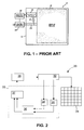
- EP 1 158 483 a system 10 is described which corrects for the aging of the pixels in a display.
- the system 10 comprises a solid-state display device 12.
- the system 10 uses reference pixels 14 to enable the measurement of pixel performance and a feedback mechanism responsive to the measured pixel performance to modify the operating characteristics of the display device 10 (see Fig. 1).
- the characteristics of the reference pixels 14 are measured by a measurement circuit 18 and the information gathered thereby is connected to an analysis circuit 20.
- the analysis circuit 20 produces a feedback signal that is supplied to a control circuit 22.
- the control circuit 22 modifies the operating characteristics of the image display 10 through control lines 24.
- the measurement circuit 18 monitors the performance of the reference pixel 14.
- the measured performance values are compared to the expected or desired performance by the analysis circuit 20. These comparisons can be based on a priori knowledge of the characteristics of the device 12 or simply compared to some arbitrary value empirically shown to give good performance. In either case, once a determination is made that the performance of the device 12 needs to be modified, the analysis circuitry 20 signals the feedback and control mechanism which then initiates the change.
- the present invention provides a display board comprising an array of addressable light emitting elements and driving means for driving the light emitting elements with image data.
- the display board furthermore comprises aging determination means comprising:
- Light representative of the light emitted by the light emitting elements may be light emitted by the light emitting elements themselves. Alternatively, this may be light emitted by a reference light emitting element.
- the light emitting elements and the at least one reference light emitting element may be of different types, i.e. light emitting elements having different performance properties.
- the light emitting elements of the display board may be power LEDs and the at least one reference light emitting element may be a cheaper type of LEDs such as SMD LEDs.
- the light emitting elements of the display board and the at least one reference light emitting element may be of the same type, i.e. have same performance properties. They may for example be both power LEDs, or they may both be SMD LEDs.
- the present invention provides a display board comprising an array of addressable light emitting elements and driving means for driving the light emitting elements with image data.
- the display board furthermore comprises aging determination means comprising:
- first moments in time is meant the moments at which the display is running, in other words, when the light emitting elements of the array are driven with image data.
- second moments in time is meant the moments at which intermediate calibrations are performed.
- An advantage of the display board according to embodiments of the invention is that both the reference and the aged value are determined on a same display board. This leads to more reliable and more correct determination of aging with respect to prior art devices where the aged value is compared to pre-determined values.
- the value derived from the image data may be an average value of the image data.
- the display board may furthermore comprise compensation means for compensating the light emitting elements in the array for aging based on the decision on aging.
- the compensation means may also be located outside the display board.
- An advantage hereof is that at every moment in time, compensation for aging differences between the light emitting elements of the array can be performed.
- the display board may furthermore comprise a controller for controlling the driving means.
- the array of flight emitting elements may be provided at a first side of the display board and the first and second reference light emitting elements may be provided at a second side of the display board, the second side being opposite to the first side.
- An advantage hereof is that adding the first and second reference light emitting elements does not alter the size of the display board a nd does not disturb the image as it is not part of the array of display elements.
- the array of light emitting elements may be provided at a first side of the display board and the first reference light emitting element may be provided at the first side of the display board and the second reference light emitting element may be provided at a second side of the display board, the second side being opposite to the first side.
- the first and second reference light emitting elements may be provided at a same side of the display board as the array of light emitting elements.
- the first reference light emitting device may be part of the array of light emitting devices.
- the first and second reference light emitting elements may be coupled to a same light measurement means.
- An advantage hereof is that there is not only compensated for aging of the display light emitting elements, but that there is also compensated for aging drift of the light measurement means, e.g. photodiode or phototransistor. This is because if the difference is made between the measurements both performed by a same light measurement means, possible errors emanating from the light measurement means can be exclude excluded.
- the light measurement means e.g. photodiode or phototransistor.
- the light measurement means may comprise at least one photodetector or phototransistor.
- the display board may comprise light emitting elements of different colours and a first and a second reference light emitting element may be provided for each colour.
- the display board may comprise multi-coloured light emitting elements and the aging determination means may comprise one first and one second reference light emitting element, the first and second light emitting elements being multi-coloured light emitting elements.
- the light emitting elements of the array may be LEDs.
- the display board according to embodiments of the invention may be incorporated in a display tile.
- a plurality of display tiles may form a display.
- the present invention provides a method for determining aging of a display board, the display board comprising an array of light emitting elements, driving means for driving the light emitting elements with image data, and at least one reference light emitting element.
- the method comprises:
- a reference light emitting element essentially not driven, so not showing ageing effect is on-board of the display board.
- Such reference light emitting element may be of the same type or of different type compared to the light emitting elements of the display board.
- Measuring light representative of the light emitted by the light emitting elements may comprise measuring light emitted by the light emitting elements themselves.
- measuring light representative of the light emitted by the light emitting elements may comprise measuring light emitted by a reference light emitting element.
- a method for determining aging of a display board, the display board comprising an array of light emitting elements, driving means for driving the light emitting elements with image data and at least a first and second reference light emitting elements. The method comprises:
- An advantage of the method according to embodiments of the invention is that both the reference and the aged value are determined on a same display board. This leads to more reliable and more correct determination of aging with respect to prior art devices where the aged value is compared to pre-determined values.
- the first calibration data may be equal to or may be different from the second calibration data.
- the method may comprise before driving the first and second reference light emitting elements with first and second reference data respectively, driving the light emitting elements of the display board with image data and driving the first reference light emitting element with a value derived from the image data.
- the value derived from the image data may be an average value of image data.
- a method for calibrating a display board comprising an array of light emitting elements.
- the method comprises:
- Compensating the light emitting element in the array for aging may be performed by adapting a driving parameter of the light emitting elements of the array.
- the driving parameter may be a voltage
- the driving parameter may be a current.
- light in the present invention is meant electromagnetic radiation with a wavelength between 375 and 1 000 nm, i.e. visible light, IR radiation, near IR and UV radiation.
- the present invention in embodiments thereof, provides a display board comprising an array of light emitting elements, e.g. LEDs, and age determination means, as well as a method for detecting aging of a display board.
- the method according to embodiments of the present invention yields data which can then be used for adapting the driving of the light emitting elements of the array, e.g. LEDs, so as to correct for decreasing light intensity because of aging of the light emitting elements, e.g. LEDs, of the array.
- Embodiments of the present invention may be applied to passive or active matrix displays and to monochrome or colour displays.
- the displays may be flat or curved displays.
- the boards and/or tiles optionally used in such displays may be flat or curved themselves as well.
- an array of light emitting elements e.g. LEDs
- a structure in which the light emitting elements, e.g. LEDs, are logically organised in rows and columns.
- the terms “column” and “row” are used to describe sets of the array of light emitting elements, e.g. LEDs, which are linked together.
- the linking can be in the form of a Cartesian array of rows and columns however the present invention is not limited thereto. As will be understood by those skilled in the art, columns and rows can be easily interchanged and it is intended in this disclosure that these terms be interchangeable. Also, non-Cartesian arrays may be constructed and are included within the scope of the invention.
- Each display element e.g. LED
- display boards may comprise current addressed or voltage addressed light emitting elements, e.g. LEDs.
- ELs electrostatic devices
- TFELs thin films ELs
- LEDs light emitting diodes
- OLEDs organic light emitting diodes
- PLEDs polymeric light emitting diodes
- the present invention will mainly be described with reference to LED's but the present invention is not limited thereto.
- An embodiment of the present invention provides a display board 30 comprising an array of light emitting elements such as LEDs 31, driving means 32 for driving the LEDs 31 with image data and aging determination means 33.
- the aging determination means 33 comprises at least a first reference LED 34 and a second reference LED 35.
- the first and second reference LED 34, 35 may most preferably be from a same batch as the LEDs 31 of the array on the display board 30.
- the first reference LED 34 is, during functioning of the display board 30, driven with reference data equal to a value derived from the image data for driving the LEDs 31 of the array e.g. by means of an algorithm on the display board 30.
- the algorithm may comprise deriving an average value of the image data.
- the algorithm may comprise deriving a peak value of the image data.
- the algorithm may comprise deriving a combination of a peak value and an average value, or in other words off-setting an average value of the image data with a peak value of the image data.
- reference data for driving the first reference LED 34 will be referred to as being equal to an average of the image data for driving the LEDs 31 of the array.
- the first reference LED 34 has substantially the same usage, and thus shows substantially the same aging, as the LEDs 31 of the array on the display board 30.
- the first reference LED 34 may also be called an average LED. This first reference LED 34 corresponds, throughout the useful life of the display board 30, with the average actual history of the LEDs 31.
- the first reference LED 34 is driven with first calibration data.
- the second reference LED 35 is normally not used. This LED 35 corresponds with a LED with the initial state of the LEDs 31 of the display board 30. This means that, during functioning of the display board 30, when the LEDs 31 of the array on the display board 30 are in use and thus when the first reference LED 34 is driven with reference data equal to a value derived from the image data for driving the LEDs 31 of the array by means of an algorithm, the second reference LED 35 is not driven.
- the second reference LED 35 is only used at intermediate calibration time and is then driven with second calibration data.
- the second reference LED 35 is a LED which corresponds with the "new state" of the LEDs 31 of the array on the display board 30 at the time of factory calibration.
- the first and second calibration data may be the same or may be different.
- the outputs of the first and second reference LED 34, 35 can be different.
- This difference is a calibration difference and is not attributed to aging, but should be corrected for when determining aging of the LEDs 31 of the array. Correction for the calibration difference can be done by means of specific software.
- the aging determination means 33 furthermore comprises light measurement means 36 for, during intermediate calibration, measuring light emitted by the first and second reference LED 34, 35 and comparison means 37 for comparing light emitted by the first reference LED 34 with light emitted by the second reference LED 35 and for, based on the comparison result, deciding on aging of the LEDs 31 of the array on the display board 30.
- the light measurement means 36 are adapted for measuring the brightness levels of the first and second reference LEDs 34, 35.
- the light measurement means 36 may be photodiodes.
- the light measurement means preferably have an optical transfert curve which is as flat as possible over the spectrum to be measured. The measurement resolution is preferably high enough to measure small enough differences between radiated light of the first and second reference LEDs 34, 35.
- Fig. 7 schematically illustrates the principle of embodiments of the present invention.
- the display board 30 comprising an array of LEDs 31 is driven with image data by driving means 32.
- driving means 32 also drives the first reference LED 34 with reference data which equals to an average of the image data for driving the LEDs 31 of the array.
- an intermediate calibration of the LEDs 31 of the array on the display board 30 may be performed.
- the first reference LED 34 is driven with first calibration data and light emitted by the first reference LED 34 is measured by a first light measurement means 36, which may, for example, be a photodetector, a phototransistor, a photoelectric cell, a photodiode, ....
- a first light measurement means 36 which may, for example, be a photodetector, a phototransistor, a photoelectric cell, a photodiode, ....
- the second reference LED 35 is driven with second calibration data and light emitted by the second reference LED 35 is measured by a second light measurement means, which may, for example, be a photodetector, a phototransistor, a photoelectric cell, a photodiode, ....
- the first calibration data is equal to the second calibration data, although in principle both could be different.
- the first and second light measurement means may be the same.
- the first and second reference LED 34, 35 may each be coupled to a different light measurement means. It has to be noted that when, according to embodiments of the invention, the outputs of the first and second reference LED 34, 35 is measured with a different light measurement means 36, the steps of driving and measuring the first reference LED 34 may be done in parallel to the steps of driving and measuring the second reference LED 35.
- the steps of driving and measuring the first and second reference LED 34, 35 cannot be done in parallel and the driving and measuring the first reference LED 34 may be performed before driving and measuring the second reference LED 35 or vice versa.
- the light emitted by the first reference LED 34 is compared to the light emitted by the second reference LED 35 by comparison means 37.
- the difference between the light emitted by the first reference LED 34 and the light emitted by the second reference LED 35 is an indication for the aging status of the LEDs 31 of the array on the display board 30.
- the difference between the light emitted by the first reference LED 34 and the light emitted by the second reference LED 35 obtained as described above may then be used to correct overall calibration values for adapting the driving parameter of the LEDs 31, bringing the actual LED aging into account.
- This can be done by changing the driving parameter of the driving means 32 by means of controller 38.
- correction for aging may be done by adapting the voltage the LEDs 31 are driven with based on the calibration values, such that no loss of brightness occurs because of aging of the LEDs 31.
- the current the LEDs 31 are driven with may be adapted based on the calibration values, such that no loss of brightness occurs because of aging of the LEDs 31.
- An advantage of the display board 30 and method according to embodiments of the present invention is that both the light emitted by the first reference LED 34 and the light emitted by the second reference LED 35 are determined on a same display board 30 or in other words, are both measured under the same circumstances. Therefore, compared to the prior art where the light emitted by a reference LED is compared with an a priori knowledge of the characteristics of the device or simply compared to some arbitrary value empirically shown to give good performance, embodiments of the present invention may lead to more reliable and up to date determination and thus of subsequent compensation for the aging problem of the LEDs 31.
- An additional advantage of particular embodiments i.e. the embodiments where the light emitted by the first reference LED 34 is measured by the same light measurement means 36 as the light emitted by the second reference LED 35 is that also can be compensated for aging drift of the light measurement means 36, e.g. photodetector, phototransistor, photoelectric cell, photodiode, ..., because the drift on this component is always re-normalized by making the difference between the light emitted by the first reference LED 34 and measured by the light measurement means 36 and light emitted by the second reference LED 35 and measured by the same light measurement means 36.
- drift on this component is always re-normalized by making the difference between the light emitted by the first reference LED 34 and measured by the light measurement means 36 and light emitted by the second reference LED 35 and measured by the same light measurement means 36.
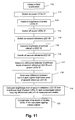
- Phase 1 is the initial phase, illustrated in the flow chart of Fig. 8. This is the measurement and calibration phase (color and brightness) of the board 30.
- the first and second reference light emitting elements, e.g. LEDs 34, 35 are driven at a same level as the display light emitting elements, e.g. LEDs 31.
- the initial brightness of the first and second reference LEDs 34, 35 is measured, steps 82 and 83, and optionally stored. From the measured initial brightness values, an optical coupling difference between both measurements is determined as a constant error value, step 84.
- This process determines the initial difference between the first and second reference LEDs 34, 35, which includes brightness differences between first and second reference LEDs 34, 35 at the same drive parameters and the difference measured by the measurement means 36 because of different optical coupling from the first reference LED 34 to the measurement means 36 and the second reference LED 35 to the measurement means 36, step 84.
- Phase 2 is the normal life of the display board 30.
- the first reference LED 34 is driven with reference data equal to a value derived from the image data for driving the LEDs 31 of the array e.g. is driven at the average value of the display LEDs 31.
- the second reference LED 35 is not driven. This second reference LED will only be used when field recalibration is executed.
- Phase 3 is the in-field recalibration phase, illustrated in the flow chart of Fig. 9.
- the display LEDs 31 have aged significantly, because of usage/runtime of the display board 30 up to the level of visibility.
- An aim of embodiments of the present invention is to get the display LEDs 31 back to their initial factory performance.
- Phase 3 of the process the in-field recalibration process, can be initiated, step 90.
- the first and second reference LEDs 34, 35 are driven in the same way for the different colours, e.g. R, G, B and W.
- the first reference LED 34 is switched on, step 91, and its brightness is measured, step 92, after which the first reference LED is switched off, step 93.
- the second reference LED 35 is switched on, step 94, and its brightness is measured, step 95, after which the first reference LED is switched off, step 96.
- the brightness of first and second reference LEDs 34, 35 may be measured one after the other, either of these being measured first. Alternatively, if two separate measurement means 36 are used for measuring brightness of first and second reference LEDs 34, 35, the measurements can be performed in parallel.
- the difference between the brightness levels of first and second reference LEDs 34, 35 is determined, step 97. Since the second reference LED 35 has never been used, it intrinsically represents the initial state of the display LEDs 31 at 0-hours life. Since the first reference LED 34 has been driven with reference data equal to a value derived from the image data for driving the LEDs 31 of the array e.g.
- the reference LED 34 has substantially the same usage, and thus shows substantially the same aging as the LEDs 31 of the array on the display board 30.
- the difference between the light emitted by the first reference LED 34 and the light emitted by the second reference LED 35 is an indication for the aging status of the LEDs 31 of the array on the display board 30.
- measurement means 36 can change property over time and temperature. Since the initial difference between first and second reference LEDs 34, 35 is known from phase 1, as well as the optical measurement difference of the measurement values of the measurement means 36 for the first and second reference LEDs 34, 35, a compensation for the optical differences of the measurement device 36 can be made, step 98, and the resulting aging can be calculated.
- the driving parameters of display LEDs 31 can be compensated for the determined ageing.
- a concept of embodiments of the method is that the actual initial reference is on board of the display board 30 (by means of the second reference LED 35) and by re-measuring the second reference LED 35 during an in-field recalibration, the electrical drift of the measurement means 36 is eliminated.
- the only difference between measurements is then the optical difference caused by the difference in light coupling between first reference LED 34 / optical measurement means 36 and second reference LED 35 / optical measurement means 36. Since the latter is constant, the difference in aging between first and second reference LEDs 34, 35 remains.
- the adjustment results in a level 1 adjustment on the display board 30 LEDs 31 and the drive levels of the first and second reference LEDs 34, 35.
- the at least first and second reference LED 34, 35 may be provided at a side of the display board 30 opposite to the side of the display board 30 where the image is shown intended to be looked at. This is illustrated in Figs. 3A and 3B which respectively show a front side and a back side of a display board 30 according to embodiments of the invention. In Fig. 3B, for reasons of simplicity, only the first and second reference LED 34, 35 and the light measurement means 36 are illustrated. Most preferably, as already discussed above, the first and second reference LED 34, 35 may be coupled to a same light measurement means 36 which is for measuring light emitted by the first and second reference LED 34, 35 when driven by respectively first and second calibration data. According to other embodiments, however, the first and second reference LED 34, 35 may each be coupled to a different light measurement means 36.
- An advantage of the example illustrated in Fig. 3A and 3B is that the provision of aging determination means 33 does not alter the size of the display board 30 because it is provided at the backside of the display board 30. Furthermore, the provision of at least a first and second reference LED 34, 35 does not disturb the image provided at the display board 30 because none of the at least first and second reference LEDs 34, 35 is part of the array of LEDs 31 on the display board 30.
- FIG. 3A and 3B Another advantage of the embodiments illustrated in Figs. 3A and 3B is that they can more easily be used in tiled displays.
- the first reference LED 34 may be a LED which is part of the array of LEDs 31 at the front side of the display board 30 and may thus also be provided at the front side of the display board 30 (see Fig. 4A).
- the second reference LED 35 may be provided at the side opposite to the side where the first reference LED 34 is provided and may thus be provided at the back of the display board 30 (see Fig. 4B).
- both the first and second reference LED 34, 35 may most preferably be coupled to a same light measurement means 36, which preferably is located at the backside of the display board 30.
- the first reference LED 35 may be coupled to the light measurement means 36 by, for example, a light pipe (not shown in the figures) for coupling the light emitted by the first reference LED 34 from the front side of the display board 30 to the backside of the display board 30.
- the first and second reference LED 34, 35 may each be coupled to a different light measurement means 36 which may be located at the front side or the back side of the display.
- the first and second reference LED 34, 35 may both be provided at the same side of the display board 30 as the array of LEDs 31.
- the first reference LED 34 may, similarly to the embodiment illustrated in Fig. 4A and 4B, be formed by a LED which is part of the array of L EDs 31 on the display board 3 0.
- the second reference LED 35 may be provided next to the array of LEDs 31, also at the front side of the display board 30.
- the part next to the array of LEDs 31 where the second reference LED 35 is provided may, according to embodiments of the invention, be covered so as to hide the reference LED 35 (not shown).
- both the first and second reference LED 34, 35 are coupled to a same light measurement means 36 which may preferably be provided next to the array of LEDs 31, as illustrated in Fig. 5. According to other embodiments, the first and second reference LED 34, 35 may each be coupled to a different light measurement means 36.
- the first reference LED 34 which is driven by reference data equal to an average of the image data the LEDs 31 of the array are driven with, is formed by a LED which is part of the array. Hence, this may disturb the image formed on the display board 30. In order to avoid this, the first reference LED 34 could be hidden from direct view, e.g. by a non-transparent covering means.
- both the first and second reference LED 34, 35 may be provided at the front side of the display board 30 next to the array of LEDs 31, as illustrated in Fig. 6. Most preferably, both the first and second reference LED 34, 35 may be coupled to a same light measurement means 36. According to other embodiments, the first and second reference LED 34, 35 may each be coupled to another light measurement means 36.
- the display board 30 according to the embodiment illustrated in Fig. 6 has the disadvantage that the provision of aging determination means 33 to the display board 30 alters the size of the display board 30. However, because none of the first or second reference LED 34, 35 is part of the array of LEDs 31, the provision of the age determination means 32 will not disturb in any way the image provided by the display board 30.
- the edges of the display board 30 may be covered by a cover 39, as illustrated in Fig. 6. In that way, the first and second reference LED 34, 35 and the light measurement means 36 may be covered and thus may be hidden and may be protected against environmental influences.
- the above-described embodiments all relate to display boards 30 comprising one kind of LEDs, i.e. all the LEDs on the display board 30 are of a same colour and thus the above-described embodiments relate to monochrome display boards and thus only require one first and one second reference LED 34, 35.
- the display board 30 may comprise LEDs 31 of different colours. It is known that LEDs 31 with different colours age in a different way. Therefore, the aging determination means 33 may comprise a first reference LED 34 and a second reference LED 35 for each colour. For example, if the display board 30 comprises red, green and blue LEDs the aging determination means 33 may comprise a red first and second reference LED, a green first and second reference LED and a blue first and second reference LED.
- the display board 3 0 m ay comprise multi-colour LEDs, each LED comprising e.g. three colours.
- the first and second reference LEDs 34, 35 being the same multi-colour LEDs as the multi-colour LEDs 31 of the array on the display board 30.
- the display LEDs 31 may be power LEDs, as typically applied in display applications, e.g. outdoor display applications, where LEDs are used to form the pixels of the display board 30. Most often it is too expensive to provide, on top of the display LEDs 31 also first and second reference LEDs 34, 35 as power LEDs, as such power LEDs are much more expensive than other LEDs. Of course, if there is no objection to extend the display board 30 to carry first and second reference "power LEDs" 34, 35, the basic principle of aging compensation as in embodiments of the present invention set o ut a bove can be applied.
- first and second reference LEDs 34, 35 under the form of a power LED would add a significant cost to the display board 30. Therefore, first and second reference LEDs 34, 35, according to embodiments of the present invention, can be replaced by a cheaper alternative. Only one cheap reference LED needs to be provided; however, a plurality of reference LEDs may be provided. The one or more reference LEDs should show the same ageing characteristics as the display LEDs 31. This embodiment requires that the measurement means 36 can sample the light of the power LEDs 31 and also the light of the cheaper reference LED 35. The process again comprises 3 phases:
- the measurement result of the second reference LED 35 is compared with the original value, step 118, which may have been stored in a memory. The difference between these values determines the drift of the measurement means 36, which can also be used for the power LED measurements.
- the difference between brightness levels of the second reference LED 35 and power LEDs 31 is determined, step 117.
- the brightness level of the second reference LED 35 is compared to the brightness level of the power LEDs 31, step 119.
- a compensation for optical coupling differences may be made. Measuring both values of the power LEDs 31 and the second reference LEDs 35 with the same measurement means 36 fully eliminates drifts of the measurement means 36.
- the optical coupling difference is known and constant over life, and is taken into account in the compensation calculation, yielding a correction of the drive of the power LEDs 31 in order to compensate for their aging (and thus run-time), step 120.
Landscapes
- Engineering & Computer Science (AREA)
- Physics & Mathematics (AREA)
- Computer Hardware Design (AREA)
- General Physics & Mathematics (AREA)
- Theoretical Computer Science (AREA)
- Control Of Indicators Other Than Cathode Ray Tubes (AREA)
- Electroluminescent Light Sources (AREA)
Priority Applications (1)
| Application Number | Priority Date | Filing Date | Title |
|---|---|---|---|
| EP07013567A EP1879172A1 (fr) | 2006-07-14 | 2007-07-11 | Compensation de vieillissement des tableaux d'affichage comprenant des éléments émettant de la lumière |
Applications Claiming Priority (2)
| Application Number | Priority Date | Filing Date | Title |
|---|---|---|---|
| EP06014750A EP1879169A1 (fr) | 2006-07-14 | 2006-07-14 | Compensation de vieillissement des tableaux d'affichage comprenant des éléments émettant de la lumière |
| EP07013567A EP1879172A1 (fr) | 2006-07-14 | 2007-07-11 | Compensation de vieillissement des tableaux d'affichage comprenant des éléments émettant de la lumière |
Publications (1)
| Publication Number | Publication Date |
|---|---|
| EP1879172A1 true EP1879172A1 (fr) | 2008-01-16 |
Family
ID=38820113
Family Applications (1)
| Application Number | Title | Priority Date | Filing Date |
|---|---|---|---|
| EP07013567A Withdrawn EP1879172A1 (fr) | 2006-07-14 | 2007-07-11 | Compensation de vieillissement des tableaux d'affichage comprenant des éléments émettant de la lumière |
Country Status (1)
| Country | Link |
|---|---|
| EP (1) | EP1879172A1 (fr) |
Cited By (58)
| Publication number | Priority date | Publication date | Assignee | Title |
|---|---|---|---|---|
| CN102665366A (zh) * | 2012-04-17 | 2012-09-12 | 四川新力光源有限公司 | Led照明灯具的故障检测系统 |
| EP2531996A4 (fr) * | 2010-02-04 | 2013-09-04 | Ignis Innovation Inc | Système et procédés pour extraire des courbes de corrélation d'un dispositif électroluminescent organique |
| WO2014079131A1 (fr) | 2012-11-21 | 2014-05-30 | Lighthouse Technologies Limited | Réglage automatique de couleur sur un écran vidéo à del |
| US8743096B2 (en) | 2006-04-19 | 2014-06-03 | Ignis Innovation, Inc. | Stable driving scheme for active matrix displays |
| US8816946B2 (en) | 2004-12-15 | 2014-08-26 | Ignis Innovation Inc. | Method and system for programming, calibrating and driving a light emitting device display |
| US8907991B2 (en) | 2010-12-02 | 2014-12-09 | Ignis Innovation Inc. | System and methods for thermal compensation in AMOLED displays |
| USRE45291E1 (en) | 2004-06-29 | 2014-12-16 | Ignis Innovation Inc. | Voltage-programming scheme for current-driven AMOLED displays |
| US8922544B2 (en) | 2012-05-23 | 2014-12-30 | Ignis Innovation Inc. | Display systems with compensation for line propagation delay |
| US8941697B2 (en) | 2003-09-23 | 2015-01-27 | Ignis Innovation Inc. | Circuit and method for driving an array of light emitting pixels |
| US8994617B2 (en) | 2010-03-17 | 2015-03-31 | Ignis Innovation Inc. | Lifetime uniformity parameter extraction methods |
| US9059117B2 (en) | 2009-12-01 | 2015-06-16 | Ignis Innovation Inc. | High resolution pixel architecture |
| US9093028B2 (en) | 2009-12-06 | 2015-07-28 | Ignis Innovation Inc. | System and methods for power conservation for AMOLED pixel drivers |
| US9093029B2 (en) | 2011-05-20 | 2015-07-28 | Ignis Innovation Inc. | System and methods for extraction of threshold and mobility parameters in AMOLED displays |
| US9111485B2 (en) | 2009-06-16 | 2015-08-18 | Ignis Innovation Inc. | Compensation technique for color shift in displays |
| US9125278B2 (en) | 2006-08-15 | 2015-09-01 | Ignis Innovation Inc. | OLED luminance degradation compensation |
| US9171500B2 (en) | 2011-05-20 | 2015-10-27 | Ignis Innovation Inc. | System and methods for extraction of parasitic parameters in AMOLED displays |
| US9171504B2 (en) | 2013-01-14 | 2015-10-27 | Ignis Innovation Inc. | Driving scheme for emissive displays providing compensation for driving transistor variations |
| US9275579B2 (en) | 2004-12-15 | 2016-03-01 | Ignis Innovation Inc. | System and methods for extraction of threshold and mobility parameters in AMOLED displays |
| US9280933B2 (en) | 2004-12-15 | 2016-03-08 | Ignis Innovation Inc. | System and methods for extraction of threshold and mobility parameters in AMOLED displays |
| US9305488B2 (en) | 2013-03-14 | 2016-04-05 | Ignis Innovation Inc. | Re-interpolation with edge detection for extracting an aging pattern for AMOLED displays |
| US9311859B2 (en) | 2009-11-30 | 2016-04-12 | Ignis Innovation Inc. | Resetting cycle for aging compensation in AMOLED displays |
| US9324268B2 (en) | 2013-03-15 | 2016-04-26 | Ignis Innovation Inc. | Amoled displays with multiple readout circuits |
| US9336717B2 (en) | 2012-12-11 | 2016-05-10 | Ignis Innovation Inc. | Pixel circuits for AMOLED displays |
| US9343006B2 (en) | 2012-02-03 | 2016-05-17 | Ignis Innovation Inc. | Driving system for active-matrix displays |
| US9384698B2 (en) | 2009-11-30 | 2016-07-05 | Ignis Innovation Inc. | System and methods for aging compensation in AMOLED displays |
| US9437137B2 (en) | 2013-08-12 | 2016-09-06 | Ignis Innovation Inc. | Compensation accuracy |
| US9466240B2 (en) | 2011-05-26 | 2016-10-11 | Ignis Innovation Inc. | Adaptive feedback system for compensating for aging pixel areas with enhanced estimation speed |
| US9530349B2 (en) | 2011-05-20 | 2016-12-27 | Ignis Innovations Inc. | Charged-based compensation and parameter extraction in AMOLED displays |
| CN104470162B (zh) * | 2012-04-17 | 2017-01-25 | 四川新力光源股份有限公司 | Led照明灯具的故障检测方法 |
| US9741282B2 (en) | 2013-12-06 | 2017-08-22 | Ignis Innovation Inc. | OLED display system and method |
| US9747834B2 (en) | 2012-05-11 | 2017-08-29 | Ignis Innovation Inc. | Pixel circuits including feedback capacitors and reset capacitors, and display systems therefore |
| US9761170B2 (en) | 2013-12-06 | 2017-09-12 | Ignis Innovation Inc. | Correction for localized phenomena in an image array |
| US9773439B2 (en) | 2011-05-27 | 2017-09-26 | Ignis Innovation Inc. | Systems and methods for aging compensation in AMOLED displays |
| US9786209B2 (en) | 2009-11-30 | 2017-10-10 | Ignis Innovation Inc. | System and methods for aging compensation in AMOLED displays |
| US9786223B2 (en) | 2012-12-11 | 2017-10-10 | Ignis Innovation Inc. | Pixel circuits for AMOLED displays |
| US9799246B2 (en) | 2011-05-20 | 2017-10-24 | Ignis Innovation Inc. | System and methods for extraction of threshold and mobility parameters in AMOLED displays |
| US9830857B2 (en) | 2013-01-14 | 2017-11-28 | Ignis Innovation Inc. | Cleaning common unwanted signals from pixel measurements in emissive displays |
| US9881532B2 (en) | 2010-02-04 | 2018-01-30 | Ignis Innovation Inc. | System and method for extracting correlation curves for an organic light emitting device |
| US9947293B2 (en) | 2015-05-27 | 2018-04-17 | Ignis Innovation Inc. | Systems and methods of reduced memory bandwidth compensation |
| US10012678B2 (en) | 2004-12-15 | 2018-07-03 | Ignis Innovation Inc. | Method and system for programming, calibrating and/or compensating, and driving an LED display |
| US10013907B2 (en) | 2004-12-15 | 2018-07-03 | Ignis Innovation Inc. | Method and system for programming, calibrating and/or compensating, and driving an LED display |
| US10019941B2 (en) | 2005-09-13 | 2018-07-10 | Ignis Innovation Inc. | Compensation technique for luminance degradation in electro-luminance devices |
| US10074304B2 (en) | 2015-08-07 | 2018-09-11 | Ignis Innovation Inc. | Systems and methods of pixel calibration based on improved reference values |
| US10078984B2 (en) | 2005-02-10 | 2018-09-18 | Ignis Innovation Inc. | Driving circuit for current programmed organic light-emitting diode displays |
| US10089921B2 (en) | 2010-02-04 | 2018-10-02 | Ignis Innovation Inc. | System and methods for extracting correlation curves for an organic light emitting device |
| US10089924B2 (en) | 2011-11-29 | 2018-10-02 | Ignis Innovation Inc. | Structural and low-frequency non-uniformity compensation |
| US10163401B2 (en) | 2010-02-04 | 2018-12-25 | Ignis Innovation Inc. | System and methods for extracting correlation curves for an organic light emitting device |
| US10176736B2 (en) | 2010-02-04 | 2019-01-08 | Ignis Innovation Inc. | System and methods for extracting correlation curves for an organic light emitting device |
| US10181282B2 (en) | 2015-01-23 | 2019-01-15 | Ignis Innovation Inc. | Compensation for color variations in emissive devices |
| US10192479B2 (en) | 2014-04-08 | 2019-01-29 | Ignis Innovation Inc. | Display system using system level resources to calculate compensation parameters for a display module in a portable device |
| US10235933B2 (en) | 2005-04-12 | 2019-03-19 | Ignis Innovation Inc. | System and method for compensation of non-uniformities in light emitting device displays |
| US10311780B2 (en) | 2015-05-04 | 2019-06-04 | Ignis Innovation Inc. | Systems and methods of optical feedback |
| US10319307B2 (en) | 2009-06-16 | 2019-06-11 | Ignis Innovation Inc. | Display system with compensation techniques and/or shared level resources |
| US10388221B2 (en) | 2005-06-08 | 2019-08-20 | Ignis Innovation Inc. | Method and system for driving a light emitting device display |
| US10439159B2 (en) | 2013-12-25 | 2019-10-08 | Ignis Innovation Inc. | Electrode contacts |
| US10573231B2 (en) | 2010-02-04 | 2020-02-25 | Ignis Innovation Inc. | System and methods for extracting correlation curves for an organic light emitting device |
| US10867536B2 (en) | 2013-04-22 | 2020-12-15 | Ignis Innovation Inc. | Inspection system for OLED display panels |
| US10996258B2 (en) | 2009-11-30 | 2021-05-04 | Ignis Innovation Inc. | Defect detection and correction of pixel circuits for AMOLED displays |
Citations (6)
| Publication number | Priority date | Publication date | Assignee | Title |
|---|---|---|---|---|
| EP0425210A2 (fr) * | 1989-10-27 | 1991-05-02 | Eev Limited | Commande des propriétés visuelles d'un affichage à cristaux liquides |
| EP1158483A2 (fr) * | 2000-05-24 | 2001-11-28 | Eastman Kodak Company | Affichage à l'état solide avec pixel de référence |
| WO2002097774A2 (fr) * | 2001-06-01 | 2002-12-05 | Printable Field Emitters Limited | Electronique de commande pour dispositifs d'affichage |
| EP1335430A1 (fr) * | 2002-02-12 | 2003-08-13 | Eastman Kodak Company | Pixel pour un écran plat avec rétroaction de luminosité |
| WO2004025615A1 (fr) * | 2002-09-16 | 2004-03-25 | Koninklijke Philips Electronics N.V. | Dispositif d'affichage |
| US20060119592A1 (en) * | 2004-12-06 | 2006-06-08 | Jian Wang | Electronic device and method of using the same |
-
2007
- 2007-07-11 EP EP07013567A patent/EP1879172A1/fr not_active Withdrawn
Patent Citations (6)
| Publication number | Priority date | Publication date | Assignee | Title |
|---|---|---|---|---|
| EP0425210A2 (fr) * | 1989-10-27 | 1991-05-02 | Eev Limited | Commande des propriétés visuelles d'un affichage à cristaux liquides |
| EP1158483A2 (fr) * | 2000-05-24 | 2001-11-28 | Eastman Kodak Company | Affichage à l'état solide avec pixel de référence |
| WO2002097774A2 (fr) * | 2001-06-01 | 2002-12-05 | Printable Field Emitters Limited | Electronique de commande pour dispositifs d'affichage |
| EP1335430A1 (fr) * | 2002-02-12 | 2003-08-13 | Eastman Kodak Company | Pixel pour un écran plat avec rétroaction de luminosité |
| WO2004025615A1 (fr) * | 2002-09-16 | 2004-03-25 | Koninklijke Philips Electronics N.V. | Dispositif d'affichage |
| US20060119592A1 (en) * | 2004-12-06 | 2006-06-08 | Jian Wang | Electronic device and method of using the same |
Cited By (131)
| Publication number | Priority date | Publication date | Assignee | Title |
|---|---|---|---|---|
| US9472138B2 (en) | 2003-09-23 | 2016-10-18 | Ignis Innovation Inc. | Pixel driver circuit with load-balance in current mirror circuit |
| US9472139B2 (en) | 2003-09-23 | 2016-10-18 | Ignis Innovation Inc. | Circuit and method for driving an array of light emitting pixels |
| US9852689B2 (en) | 2003-09-23 | 2017-12-26 | Ignis Innovation Inc. | Circuit and method for driving an array of light emitting pixels |
| US8941697B2 (en) | 2003-09-23 | 2015-01-27 | Ignis Innovation Inc. | Circuit and method for driving an array of light emitting pixels |
| US10089929B2 (en) | 2003-09-23 | 2018-10-02 | Ignis Innovation Inc. | Pixel driver circuit with load-balance in current mirror circuit |
| USRE45291E1 (en) | 2004-06-29 | 2014-12-16 | Ignis Innovation Inc. | Voltage-programming scheme for current-driven AMOLED displays |
| USRE47257E1 (en) | 2004-06-29 | 2019-02-26 | Ignis Innovation Inc. | Voltage-programming scheme for current-driven AMOLED displays |
| US8994625B2 (en) | 2004-12-15 | 2015-03-31 | Ignis Innovation Inc. | Method and system for programming, calibrating and driving a light emitting device display |
| US8816946B2 (en) | 2004-12-15 | 2014-08-26 | Ignis Innovation Inc. | Method and system for programming, calibrating and driving a light emitting device display |
| US10013907B2 (en) | 2004-12-15 | 2018-07-03 | Ignis Innovation Inc. | Method and system for programming, calibrating and/or compensating, and driving an LED display |
| US9275579B2 (en) | 2004-12-15 | 2016-03-01 | Ignis Innovation Inc. | System and methods for extraction of threshold and mobility parameters in AMOLED displays |
| US10012678B2 (en) | 2004-12-15 | 2018-07-03 | Ignis Innovation Inc. | Method and system for programming, calibrating and/or compensating, and driving an LED display |
| US9970964B2 (en) | 2004-12-15 | 2018-05-15 | Ignis Innovation Inc. | Method and system for programming, calibrating and driving a light emitting device display |
| US10699624B2 (en) | 2004-12-15 | 2020-06-30 | Ignis Innovation Inc. | Method and system for programming, calibrating and/or compensating, and driving an LED display |
| US9280933B2 (en) | 2004-12-15 | 2016-03-08 | Ignis Innovation Inc. | System and methods for extraction of threshold and mobility parameters in AMOLED displays |
| US10078984B2 (en) | 2005-02-10 | 2018-09-18 | Ignis Innovation Inc. | Driving circuit for current programmed organic light-emitting diode displays |
| US10235933B2 (en) | 2005-04-12 | 2019-03-19 | Ignis Innovation Inc. | System and method for compensation of non-uniformities in light emitting device displays |
| US10388221B2 (en) | 2005-06-08 | 2019-08-20 | Ignis Innovation Inc. | Method and system for driving a light emitting device display |
| US10019941B2 (en) | 2005-09-13 | 2018-07-10 | Ignis Innovation Inc. | Compensation technique for luminance degradation in electro-luminance devices |
| US9842544B2 (en) | 2006-04-19 | 2017-12-12 | Ignis Innovation Inc. | Stable driving scheme for active matrix displays |
| US10453397B2 (en) | 2006-04-19 | 2019-10-22 | Ignis Innovation Inc. | Stable driving scheme for active matrix displays |
| US10127860B2 (en) | 2006-04-19 | 2018-11-13 | Ignis Innovation Inc. | Stable driving scheme for active matrix displays |
| US9633597B2 (en) | 2006-04-19 | 2017-04-25 | Ignis Innovation Inc. | Stable driving scheme for active matrix displays |
| US8743096B2 (en) | 2006-04-19 | 2014-06-03 | Ignis Innovation, Inc. | Stable driving scheme for active matrix displays |
| US9125278B2 (en) | 2006-08-15 | 2015-09-01 | Ignis Innovation Inc. | OLED luminance degradation compensation |
| US9530352B2 (en) | 2006-08-15 | 2016-12-27 | Ignis Innovations Inc. | OLED luminance degradation compensation |
| US10325554B2 (en) | 2006-08-15 | 2019-06-18 | Ignis Innovation Inc. | OLED luminance degradation compensation |
| US9111485B2 (en) | 2009-06-16 | 2015-08-18 | Ignis Innovation Inc. | Compensation technique for color shift in displays |
| US9418587B2 (en) | 2009-06-16 | 2016-08-16 | Ignis Innovation Inc. | Compensation technique for color shift in displays |
| US10319307B2 (en) | 2009-06-16 | 2019-06-11 | Ignis Innovation Inc. | Display system with compensation techniques and/or shared level resources |
| US9117400B2 (en) | 2009-06-16 | 2015-08-25 | Ignis Innovation Inc. | Compensation technique for color shift in displays |
| US10553141B2 (en) | 2009-06-16 | 2020-02-04 | Ignis Innovation Inc. | Compensation technique for color shift in displays |
| US9311859B2 (en) | 2009-11-30 | 2016-04-12 | Ignis Innovation Inc. | Resetting cycle for aging compensation in AMOLED displays |
| US10304390B2 (en) | 2009-11-30 | 2019-05-28 | Ignis Innovation Inc. | System and methods for aging compensation in AMOLED displays |
| US10699613B2 (en) | 2009-11-30 | 2020-06-30 | Ignis Innovation Inc. | Resetting cycle for aging compensation in AMOLED displays |
| US9786209B2 (en) | 2009-11-30 | 2017-10-10 | Ignis Innovation Inc. | System and methods for aging compensation in AMOLED displays |
| US9384698B2 (en) | 2009-11-30 | 2016-07-05 | Ignis Innovation Inc. | System and methods for aging compensation in AMOLED displays |
| US10996258B2 (en) | 2009-11-30 | 2021-05-04 | Ignis Innovation Inc. | Defect detection and correction of pixel circuits for AMOLED displays |
| US10679533B2 (en) | 2009-11-30 | 2020-06-09 | Ignis Innovation Inc. | System and methods for aging compensation in AMOLED displays |
| US9059117B2 (en) | 2009-12-01 | 2015-06-16 | Ignis Innovation Inc. | High resolution pixel architecture |
| US9093028B2 (en) | 2009-12-06 | 2015-07-28 | Ignis Innovation Inc. | System and methods for power conservation for AMOLED pixel drivers |
| US9262965B2 (en) | 2009-12-06 | 2016-02-16 | Ignis Innovation Inc. | System and methods for power conservation for AMOLED pixel drivers |
| US10176736B2 (en) | 2010-02-04 | 2019-01-08 | Ignis Innovation Inc. | System and methods for extracting correlation curves for an organic light emitting device |
| US10089921B2 (en) | 2010-02-04 | 2018-10-02 | Ignis Innovation Inc. | System and methods for extracting correlation curves for an organic light emitting device |
| US10971043B2 (en) | 2010-02-04 | 2021-04-06 | Ignis Innovation Inc. | System and method for extracting correlation curves for an organic light emitting device |
| US8589100B2 (en) | 2010-02-04 | 2013-11-19 | Ignis Innovation Inc. | System and methods for extracting correlation curves for an organic light emitting device |
| US10163401B2 (en) | 2010-02-04 | 2018-12-25 | Ignis Innovation Inc. | System and methods for extracting correlation curves for an organic light emitting device |
| US11200839B2 (en) | 2010-02-04 | 2021-12-14 | Ignis Innovation Inc. | System and methods for extracting correlation curves for an organic light emitting device |
| US10573231B2 (en) | 2010-02-04 | 2020-02-25 | Ignis Innovation Inc. | System and methods for extracting correlation curves for an organic light emitting device |
| EP2531996A4 (fr) * | 2010-02-04 | 2013-09-04 | Ignis Innovation Inc | Système et procédés pour extraire des courbes de corrélation d'un dispositif électroluminescent organique |
| US10032399B2 (en) | 2010-02-04 | 2018-07-24 | Ignis Innovation Inc. | System and methods for extracting correlation curves for an organic light emitting device |
| US9881532B2 (en) | 2010-02-04 | 2018-01-30 | Ignis Innovation Inc. | System and method for extracting correlation curves for an organic light emitting device |
| US10395574B2 (en) | 2010-02-04 | 2019-08-27 | Ignis Innovation Inc. | System and methods for extracting correlation curves for an organic light emitting device |
| EP3324391A1 (fr) * | 2010-02-04 | 2018-05-23 | Ignis Innovation Inc. | Système et procédés pour extraire des courbes de corrélation destinés à un dispositif électroluminescent organique |
| US9430958B2 (en) | 2010-02-04 | 2016-08-30 | Ignis Innovation Inc. | System and methods for extracting correlation curves for an organic light emitting device |
| US9773441B2 (en) | 2010-02-04 | 2017-09-26 | Ignis Innovation Inc. | System and methods for extracting correlation curves for an organic light emitting device |
| US8994617B2 (en) | 2010-03-17 | 2015-03-31 | Ignis Innovation Inc. | Lifetime uniformity parameter extraction methods |
| US9997110B2 (en) | 2010-12-02 | 2018-06-12 | Ignis Innovation Inc. | System and methods for thermal compensation in AMOLED displays |
| US9489897B2 (en) | 2010-12-02 | 2016-11-08 | Ignis Innovation Inc. | System and methods for thermal compensation in AMOLED displays |
| US10460669B2 (en) | 2010-12-02 | 2019-10-29 | Ignis Innovation Inc. | System and methods for thermal compensation in AMOLED displays |
| US8907991B2 (en) | 2010-12-02 | 2014-12-09 | Ignis Innovation Inc. | System and methods for thermal compensation in AMOLED displays |
| US9530349B2 (en) | 2011-05-20 | 2016-12-27 | Ignis Innovations Inc. | Charged-based compensation and parameter extraction in AMOLED displays |
| US9799246B2 (en) | 2011-05-20 | 2017-10-24 | Ignis Innovation Inc. | System and methods for extraction of threshold and mobility parameters in AMOLED displays |
| US10580337B2 (en) | 2011-05-20 | 2020-03-03 | Ignis Innovation Inc. | System and methods for extraction of threshold and mobility parameters in AMOLED displays |
| US10127846B2 (en) | 2011-05-20 | 2018-11-13 | Ignis Innovation Inc. | System and methods for extraction of threshold and mobility parameters in AMOLED displays |
| US9093029B2 (en) | 2011-05-20 | 2015-07-28 | Ignis Innovation Inc. | System and methods for extraction of threshold and mobility parameters in AMOLED displays |
| US10032400B2 (en) | 2011-05-20 | 2018-07-24 | Ignis Innovation Inc. | System and methods for extraction of threshold and mobility parameters in AMOLED displays |
| US9799248B2 (en) | 2011-05-20 | 2017-10-24 | Ignis Innovation Inc. | System and methods for extraction of threshold and mobility parameters in AMOLED displays |
| US9589490B2 (en) | 2011-05-20 | 2017-03-07 | Ignis Innovation Inc. | System and methods for extraction of threshold and mobility parameters in AMOLED displays |
| US9171500B2 (en) | 2011-05-20 | 2015-10-27 | Ignis Innovation Inc. | System and methods for extraction of parasitic parameters in AMOLED displays |
| US10475379B2 (en) | 2011-05-20 | 2019-11-12 | Ignis Innovation Inc. | Charged-based compensation and parameter extraction in AMOLED displays |
| US9355584B2 (en) | 2011-05-20 | 2016-05-31 | Ignis Innovation Inc. | System and methods for extraction of threshold and mobility parameters in AMOLED displays |
| US10325537B2 (en) | 2011-05-20 | 2019-06-18 | Ignis Innovation Inc. | System and methods for extraction of threshold and mobility parameters in AMOLED displays |
| US9978297B2 (en) | 2011-05-26 | 2018-05-22 | Ignis Innovation Inc. | Adaptive feedback system for compensating for aging pixel areas with enhanced estimation speed |
| US10706754B2 (en) | 2011-05-26 | 2020-07-07 | Ignis Innovation Inc. | Adaptive feedback system for compensating for aging pixel areas with enhanced estimation speed |
| US9640112B2 (en) | 2011-05-26 | 2017-05-02 | Ignis Innovation Inc. | Adaptive feedback system for compensating for aging pixel areas with enhanced estimation speed |
| US9466240B2 (en) | 2011-05-26 | 2016-10-11 | Ignis Innovation Inc. | Adaptive feedback system for compensating for aging pixel areas with enhanced estimation speed |
| US10417945B2 (en) | 2011-05-27 | 2019-09-17 | Ignis Innovation Inc. | Systems and methods for aging compensation in AMOLED displays |
| US9773439B2 (en) | 2011-05-27 | 2017-09-26 | Ignis Innovation Inc. | Systems and methods for aging compensation in AMOLED displays |
| US10380944B2 (en) | 2011-11-29 | 2019-08-13 | Ignis Innovation Inc. | Structural and low-frequency non-uniformity compensation |
| US10089924B2 (en) | 2011-11-29 | 2018-10-02 | Ignis Innovation Inc. | Structural and low-frequency non-uniformity compensation |
| US9343006B2 (en) | 2012-02-03 | 2016-05-17 | Ignis Innovation Inc. | Driving system for active-matrix displays |
| US9792857B2 (en) | 2012-02-03 | 2017-10-17 | Ignis Innovation Inc. | Driving system for active-matrix displays |
| US10453394B2 (en) | 2012-02-03 | 2019-10-22 | Ignis Innovation Inc. | Driving system for active-matrix displays |
| US10043448B2 (en) | 2012-02-03 | 2018-08-07 | Ignis Innovation Inc. | Driving system for active-matrix displays |
| CN104470162B (zh) * | 2012-04-17 | 2017-01-25 | 四川新力光源股份有限公司 | Led照明灯具的故障检测方法 |
| CN102665366A (zh) * | 2012-04-17 | 2012-09-12 | 四川新力光源有限公司 | Led照明灯具的故障检测系统 |
| CN102665366B (zh) * | 2012-04-17 | 2014-12-17 | 四川新力光源股份有限公司 | Led照明灯具的故障检测系统 |
| US9747834B2 (en) | 2012-05-11 | 2017-08-29 | Ignis Innovation Inc. | Pixel circuits including feedback capacitors and reset capacitors, and display systems therefore |
| US9536460B2 (en) | 2012-05-23 | 2017-01-03 | Ignis Innovation Inc. | Display systems with compensation for line propagation delay |
| US9368063B2 (en) | 2012-05-23 | 2016-06-14 | Ignis Innovation Inc. | Display systems with compensation for line propagation delay |
| US9940861B2 (en) | 2012-05-23 | 2018-04-10 | Ignis Innovation Inc. | Display systems with compensation for line propagation delay |
| US10176738B2 (en) | 2012-05-23 | 2019-01-08 | Ignis Innovation Inc. | Display systems with compensation for line propagation delay |
| US9741279B2 (en) | 2012-05-23 | 2017-08-22 | Ignis Innovation Inc. | Display systems with compensation for line propagation delay |
| US8922544B2 (en) | 2012-05-23 | 2014-12-30 | Ignis Innovation Inc. | Display systems with compensation for line propagation delay |
| EP2923353A4 (fr) * | 2012-11-21 | 2016-08-24 | Lighthouse Technologies Ltd | Réglage automatique de couleur sur un écran vidéo à del |
| WO2014079131A1 (fr) | 2012-11-21 | 2014-05-30 | Lighthouse Technologies Limited | Réglage automatique de couleur sur un écran vidéo à del |
| US9526141B2 (en) | 2012-11-21 | 2016-12-20 | Lighthouse Technologies Limited | Automatic color adjustment on LED screens |
| US9336717B2 (en) | 2012-12-11 | 2016-05-10 | Ignis Innovation Inc. | Pixel circuits for AMOLED displays |
| US10140925B2 (en) | 2012-12-11 | 2018-11-27 | Ignis Innovation Inc. | Pixel circuits for AMOLED displays |
| US10311790B2 (en) | 2012-12-11 | 2019-06-04 | Ignis Innovation Inc. | Pixel circuits for amoled displays |
| US9786223B2 (en) | 2012-12-11 | 2017-10-10 | Ignis Innovation Inc. | Pixel circuits for AMOLED displays |
| US9685114B2 (en) | 2012-12-11 | 2017-06-20 | Ignis Innovation Inc. | Pixel circuits for AMOLED displays |
| US9830857B2 (en) | 2013-01-14 | 2017-11-28 | Ignis Innovation Inc. | Cleaning common unwanted signals from pixel measurements in emissive displays |
| US11875744B2 (en) | 2013-01-14 | 2024-01-16 | Ignis Innovation Inc. | Cleaning common unwanted signals from pixel measurements in emissive displays |
| US9171504B2 (en) | 2013-01-14 | 2015-10-27 | Ignis Innovation Inc. | Driving scheme for emissive displays providing compensation for driving transistor variations |
| US10847087B2 (en) | 2013-01-14 | 2020-11-24 | Ignis Innovation Inc. | Cleaning common unwanted signals from pixel measurements in emissive displays |
| US9305488B2 (en) | 2013-03-14 | 2016-04-05 | Ignis Innovation Inc. | Re-interpolation with edge detection for extracting an aging pattern for AMOLED displays |
| US9536465B2 (en) | 2013-03-14 | 2017-01-03 | Ignis Innovation Inc. | Re-interpolation with edge detection for extracting an aging pattern for AMOLED displays |
| US9818323B2 (en) | 2013-03-14 | 2017-11-14 | Ignis Innovation Inc. | Re-interpolation with edge detection for extracting an aging pattern for AMOLED displays |
| US10198979B2 (en) | 2013-03-14 | 2019-02-05 | Ignis Innovation Inc. | Re-interpolation with edge detection for extracting an aging pattern for AMOLED displays |
| US9997107B2 (en) | 2013-03-15 | 2018-06-12 | Ignis Innovation Inc. | AMOLED displays with multiple readout circuits |
| US9721512B2 (en) | 2013-03-15 | 2017-08-01 | Ignis Innovation Inc. | AMOLED displays with multiple readout circuits |
| US10460660B2 (en) | 2013-03-15 | 2019-10-29 | Ingis Innovation Inc. | AMOLED displays with multiple readout circuits |
| US9324268B2 (en) | 2013-03-15 | 2016-04-26 | Ignis Innovation Inc. | Amoled displays with multiple readout circuits |
| US10867536B2 (en) | 2013-04-22 | 2020-12-15 | Ignis Innovation Inc. | Inspection system for OLED display panels |
| US9437137B2 (en) | 2013-08-12 | 2016-09-06 | Ignis Innovation Inc. | Compensation accuracy |
| US10600362B2 (en) | 2013-08-12 | 2020-03-24 | Ignis Innovation Inc. | Compensation accuracy |
| US9990882B2 (en) | 2013-08-12 | 2018-06-05 | Ignis Innovation Inc. | Compensation accuracy |
| US10186190B2 (en) | 2013-12-06 | 2019-01-22 | Ignis Innovation Inc. | Correction for localized phenomena in an image array |
| US9761170B2 (en) | 2013-12-06 | 2017-09-12 | Ignis Innovation Inc. | Correction for localized phenomena in an image array |
| US10395585B2 (en) | 2013-12-06 | 2019-08-27 | Ignis Innovation Inc. | OLED display system and method |
| US9741282B2 (en) | 2013-12-06 | 2017-08-22 | Ignis Innovation Inc. | OLED display system and method |
| US10439159B2 (en) | 2013-12-25 | 2019-10-08 | Ignis Innovation Inc. | Electrode contacts |
| US10192479B2 (en) | 2014-04-08 | 2019-01-29 | Ignis Innovation Inc. | Display system using system level resources to calculate compensation parameters for a display module in a portable device |
| US10181282B2 (en) | 2015-01-23 | 2019-01-15 | Ignis Innovation Inc. | Compensation for color variations in emissive devices |
| US10311780B2 (en) | 2015-05-04 | 2019-06-04 | Ignis Innovation Inc. | Systems and methods of optical feedback |
| US10403230B2 (en) | 2015-05-27 | 2019-09-03 | Ignis Innovation Inc. | Systems and methods of reduced memory bandwidth compensation |
| US9947293B2 (en) | 2015-05-27 | 2018-04-17 | Ignis Innovation Inc. | Systems and methods of reduced memory bandwidth compensation |
| US10074304B2 (en) | 2015-08-07 | 2018-09-11 | Ignis Innovation Inc. | Systems and methods of pixel calibration based on improved reference values |
| US10339860B2 (en) | 2015-08-07 | 2019-07-02 | Ignis Innovation, Inc. | Systems and methods of pixel calibration based on improved reference values |
Similar Documents
| Publication | Publication Date | Title |
|---|---|---|
| US8106858B2 (en) | Aging compensation for display boards comprising light emitting elements | |
| EP1879172A1 (fr) | Compensation de vieillissement des tableaux d'affichage comprenant des éléments émettant de la lumière | |
| EP1194013B1 (fr) | Ecran plat avec circuit de contrôle | |
| US8264431B2 (en) | LED array with photodetector | |
| JP5535627B2 (ja) | ピクセルの輝度劣化を補償する方法及びディスプレイ | |
| CN1682267A (zh) | 显示装置 | |
| US20050083323A1 (en) | Light emitting display device | |
| KR20060012276A (ko) | 개별적인 led 휘도 감시 능력을 갖는 led조명소스/디스플레이 및 교정 방법 | |
| US20050174309A1 (en) | Colour calibration of emissive display devices | |
| EP1565902A2 (fr) | Procede pour ameliorer l'uniformite de sortie d'un dispositif d'affichage | |
| CN101523471A (zh) | 显示器驱动系统 | |
| JP2012068659A (ja) | Oledディスプレイの経時変化補償 | |
| EP2676259B1 (fr) | Détection de variation d'émission de lumière électroluminescente | |
| KR20100015772A (ko) | 유기 el 패널의 표시 보정 회로, 표시 보정 회로 및 표시 장치 | |
| KR20060049617A (ko) | 자기 발광형 디스플레이 및 스펙트럼 내용물 조정 방법 | |
| EP2923353B1 (fr) | Réglage automatique de couleur sur un écran vidéo à del | |
| KR20040029009A (ko) | 유기 전자발광 장치에서 칼라 보정을 위한 방법 및 구동수단 | |
| WO2002097774A2 (fr) | Electronique de commande pour dispositifs d'affichage | |
| US20110169414A1 (en) | Calibration of light elements within a display | |
| US20050104821A1 (en) | Display arrangement | |
| HK1117628A (en) | Aging compensation for display boards comprising light emitting elements | |
| US20030053044A1 (en) | Color balance control in organic light emitting diode displays | |
| WO2005104075A2 (fr) | Dispositifs d'affichage, pilotes et procedes associes | |
| KR20170062571A (ko) | 표시 장치 및 그 구동 방법 | |
| JP2010026406A (ja) | 自発光型表示装置 |
Legal Events
| Date | Code | Title | Description |
|---|---|---|---|
| PUAI | Public reference made under article 153(3) epc to a published international application that has entered the european phase |
Free format text: ORIGINAL CODE: 0009012 |
|
| AK | Designated contracting states |
Kind code of ref document: A1 Designated state(s): AT BE BG CH CY CZ DE DK EE ES FI FR GB GR HU IE IS IT LI LT LU LV MC MT NL PL PT RO SE SI SK TR |
|
| AX | Request for extension of the european patent |
Extension state: AL BA HR MK YU |
|
| 17P | Request for examination filed |
Effective date: 20080612 |
|
| AKX | Designation fees paid |
Designated state(s): AT BE BG CH CY CZ DE DK EE ES FI FR GB GR HU IE IS IT LI LT LU LV MC MT NL PL PT RO SE SI SK TR |
|
| REG | Reference to a national code |
Ref country code: HK Ref legal event code: DE Ref document number: 1117628 Country of ref document: HK |
|
| 17Q | First examination report despatched |
Effective date: 20110120 |
|
| REG | Reference to a national code |
Ref country code: HK Ref legal event code: WD Ref document number: 1117628 Country of ref document: HK |
|
| STAA | Information on the status of an ep patent application or granted ep patent |
Free format text: STATUS: EXAMINATION IS IN PROGRESS |
|
| STAA | Information on the status of an ep patent application or granted ep patent |
Free format text: STATUS: THE APPLICATION IS DEEMED TO BE WITHDRAWN |
|
| 18D | Application deemed to be withdrawn |
Effective date: 20171125 |