EP1879222A2 - Verfahren zur Herstellung von Gruppe-3-Nitridsubstrat-Wafern und Gruppe-3-Nitridsubstrat-Wafer - Google Patents
Verfahren zur Herstellung von Gruppe-3-Nitridsubstrat-Wafern und Gruppe-3-Nitridsubstrat-Wafer Download PDFInfo
- Publication number
- EP1879222A2 EP1879222A2 EP07008346A EP07008346A EP1879222A2 EP 1879222 A2 EP1879222 A2 EP 1879222A2 EP 07008346 A EP07008346 A EP 07008346A EP 07008346 A EP07008346 A EP 07008346A EP 1879222 A2 EP1879222 A2 EP 1879222A2
- Authority
- EP
- European Patent Office
- Prior art keywords
- wafers
- group
- nitride substrate
- polishing plate
- wafer
- Prior art date
- Legal status (The legal status is an assumption and is not a legal conclusion. Google has not performed a legal analysis and makes no representation as to the accuracy of the status listed.)
- Withdrawn
Links
- 0 CC(CCC*)=CCC(C(CCCCCC(CCCCCCCC*)N)=C)N Chemical compound CC(CCC*)=CCC(C(CCCCCC(CCCCCCCC*)N)=C)N 0.000 description 1
Images

Classifications
-
- H—ELECTRICITY
- H10—SEMICONDUCTOR DEVICES; ELECTRIC SOLID-STATE DEVICES NOT OTHERWISE PROVIDED FOR
- H10P—GENERIC PROCESSES OR APPARATUS FOR THE MANUFACTURE OR TREATMENT OF DEVICES COVERED BY CLASS H10
- H10P52/00—Grinding, lapping or polishing of wafers, substrates or parts of devices
-
- H—ELECTRICITY
- H10—SEMICONDUCTOR DEVICES; ELECTRIC SOLID-STATE DEVICES NOT OTHERWISE PROVIDED FOR
- H10P—GENERIC PROCESSES OR APPARATUS FOR THE MANUFACTURE OR TREATMENT OF DEVICES COVERED BY CLASS H10
- H10P90/00—Preparation of wafers not covered by a single main group of this subclass, e.g. wafer reinforcement
- H10P90/12—Preparing bulk and homogeneous wafers
- H10P90/123—Preparing bulk and homogeneous wafers by grinding or lapping
-
- B—PERFORMING OPERATIONS; TRANSPORTING
- B24—GRINDING; POLISHING
- B24B—MACHINES, DEVICES, OR PROCESSES FOR GRINDING OR POLISHING; DRESSING OR CONDITIONING OF ABRADING SURFACES; FEEDING OF GRINDING, POLISHING, OR LAPPING AGENTS
- B24B37/00—Lapping machines or devices; Accessories
- B24B37/04—Lapping machines or devices; Accessories designed for working plane surfaces
- B24B37/042—Lapping machines or devices; Accessories designed for working plane surfaces operating processes therefor
-
- H—ELECTRICITY
- H10—SEMICONDUCTOR DEVICES; ELECTRIC SOLID-STATE DEVICES NOT OTHERWISE PROVIDED FOR
- H10D—INORGANIC ELECTRIC SEMICONDUCTOR DEVICES
- H10D62/00—Semiconductor bodies, or regions thereof, of devices having potential barriers
- H10D62/10—Shapes, relative sizes or dispositions of the regions of the semiconductor bodies; Shapes of the semiconductor bodies
- H10D62/117—Shapes of semiconductor bodies
-
- H—ELECTRICITY
- H10—SEMICONDUCTOR DEVICES; ELECTRIC SOLID-STATE DEVICES NOT OTHERWISE PROVIDED FOR
- H10P—GENERIC PROCESSES OR APPARATUS FOR THE MANUFACTURE OR TREATMENT OF DEVICES COVERED BY CLASS H10
- H10P14/00—Formation of materials, e.g. in the shape of layers or pillars
- H10P14/20—Formation of materials, e.g. in the shape of layers or pillars of semiconductor materials
-
- H—ELECTRICITY
- H10—SEMICONDUCTOR DEVICES; ELECTRIC SOLID-STATE DEVICES NOT OTHERWISE PROVIDED FOR
- H10P—GENERIC PROCESSES OR APPARATUS FOR THE MANUFACTURE OR TREATMENT OF DEVICES COVERED BY CLASS H10
- H10P72/00—Handling or holding of wafers, substrates or devices during manufacture or treatment thereof
- H10P72/70—Handling or holding of wafers, substrates or devices during manufacture or treatment thereof for supporting or gripping
- H10P72/74—Handling or holding of wafers, substrates or devices during manufacture or treatment thereof for supporting or gripping using temporarily an auxiliary support
-
- H—ELECTRICITY
- H10—SEMICONDUCTOR DEVICES; ELECTRIC SOLID-STATE DEVICES NOT OTHERWISE PROVIDED FOR
- H10P—GENERIC PROCESSES OR APPARATUS FOR THE MANUFACTURE OR TREATMENT OF DEVICES COVERED BY CLASS H10
- H10P90/00—Preparation of wafers not covered by a single main group of this subclass, e.g. wafer reinforcement
- H10P90/12—Preparing bulk and homogeneous wafers
- H10P90/14—Preparing bulk and homogeneous wafers by setting crystal orientation
-
- H—ELECTRICITY
- H10—SEMICONDUCTOR DEVICES; ELECTRIC SOLID-STATE DEVICES NOT OTHERWISE PROVIDED FOR
- H10W—GENERIC PACKAGES, INTERCONNECTIONS, CONNECTORS OR OTHER CONSTRUCTIONAL DETAILS OF DEVICES COVERED BY CLASS H10
- H10W46/00—Marks applied to devices, e.g. for alignment or identification
-
- H—ELECTRICITY
- H10—SEMICONDUCTOR DEVICES; ELECTRIC SOLID-STATE DEVICES NOT OTHERWISE PROVIDED FOR
- H10P—GENERIC PROCESSES OR APPARATUS FOR THE MANUFACTURE OR TREATMENT OF DEVICES COVERED BY CLASS H10
- H10P72/00—Handling or holding of wafers, substrates or devices during manufacture or treatment thereof
- H10P72/70—Handling or holding of wafers, substrates or devices during manufacture or treatment thereof for supporting or gripping
- H10P72/74—Handling or holding of wafers, substrates or devices during manufacture or treatment thereof for supporting or gripping using temporarily an auxiliary support
- H10P72/7422—Handling or holding of wafers, substrates or devices during manufacture or treatment thereof for supporting or gripping using temporarily an auxiliary support used to protect an active side of a device or wafer
-
- H—ELECTRICITY
- H10—SEMICONDUCTOR DEVICES; ELECTRIC SOLID-STATE DEVICES NOT OTHERWISE PROVIDED FOR
- H10W—GENERIC PACKAGES, INTERCONNECTIONS, CONNECTORS OR OTHER CONSTRUCTIONAL DETAILS OF DEVICES COVERED BY CLASS H10
- H10W46/00—Marks applied to devices, e.g. for alignment or identification
- H10W46/201—Marks applied to devices, e.g. for alignment or identification located on the periphery of wafers, e.g. orientation notches or lot numbers
Definitions
- This invention relates to a method of sticking as-grown GaN, AlN or AlGaN substrate wafers to a polishing plate and grinding, lapping, and polishing the as-grown wafers into mirror wafers.
- GaN, AlN and AlGaN wafers are now collectively called "group 3 nitride" wafers. All the group 3 nitride crystals cannot be grown from liquid phase.
- As-grown substrate crystals of the group 3 nitrides are produced by growing a thick film on an undersubstrate in vapor phase, eliminating the undersubstrate and obtaining a freestanding wafer.
- Silicon (Si) substrate wafers are rich in toughness. Grinding, lapping and polishing are easy for silicon wafers. GaN is more rigid than Si, but is more fragile than Si. GaN is subject to external shock far more than Si. GaN is endowed with chemical endurance higher than Si. It is difficult to etch GaN with alkalis or acids. Grinding, lapping and polishing of group 3 nitride substrate wafers are not done in a manner similar to silicon wafers. Grinding, lapping and polishing of group 3 nitride substrate wafers require special whetstones, whetting granules, polishing cloths, polishing liquids and so on.
- a one-side polishing polishes bottom surfaces of wafers by gluing object wafers on a bottom surface of a disc polishing plate (or named as a polishing holder), pushing the polishing plate on a polishing cloth of a whetting turntable, supplying a polishing liquid on the whetting turntable, rotating the polishing plate and revolving the whetting turntable.
- both surfaces should be polished by the one-side polishing, the same process shall be repeated on both surfaces of the wafers by reversing surfaces.
- Circular wafers are allotted with orientation flats (OFs) or identification flats (IFs) for designating crystallographic orientation and obverse/reverse distinction.
- orientation flats OFs
- identification flats IFs
- a plurality of GaN wafers are obtained by slicing the thick GaN ingot in the direction vertical to the growing direction.
- As-grown wafers having rugged surfaces should be finished with mirror wafers through the surface planar processing consisting of grinding, lapping and polishing.
- the present invention aims at proposing a method of grinding, lapping and polishing as-grown group 3 nitride substrate wafers.
- polishing is sometimes used as a collective word signifying planar processing including grinding, lapping and polishing briefly.
- This invention is directed to the single-surface polishing which sticks wafers on a polishing plate, pushes the polishing plate to a polishing cloth on a turntable, rotates the polishing plate, revolves the turntable and polishes the bottom surfaces of the wafers.
- An appropriate method of polishing is unknown yet, because GaN freestanding substrate wafers are novel themselves.
- GaN is more rigid than Si. Grinding, lapping and polishing of harder GaN wafers are more difficult than the planar processing of Si wafers. GaN wafers are more fragile than Si wafers, which makes more difficulty with the planar processing of GaN wafers. Small GaN crystals are useless for making devices. Wide GaN wafers are available for making devices.
- the present invention aims at wide group 3 nitride substrate wafers with a diameter of 40mm or more. GaN wafers with a 50mm diameter are especially important in the present invention.
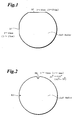
- An orientation flat is a flat edge which is produced by eliminating a bow segment from an edge of a circular wafer in order to indicate crystallographical orientation of the wafer.
- a single orientation flat is sufficient to denote the orientation.
- a one-surface mirror wafer has a rugged bottom surface, the difference of surface roughness teaches the top/bottom discrimination.
- a one-surface mirror wafer is allotted with an OF alone.
- the wafer requires two different flats for designating the orientation and the obverse/reverse discrimination.
- a longer flat is named an orientation flat (OF).
- OF is called a main flat and IF is called a sub flat.
- the eliminated parts are bow-shaped segments.
- OF and IF can be defined by lengths y, central angles T or eliminated width h alternatively, since the diameter of a circular wafer is predetermined.
- the present invention allots a 50mm diameter wafer with an OF and an IF of the following lengths.
- OF should be determined to be a (11-20) plane and IF should be determined to be a (1-100) plane in the present invention.
- a cleavage plane is (1-100) in GaN, which is parallel with IF.
- An inequality OF>IF should be kept for the lengths of OF and IF. This is the condition for discerning OF from IF. If OF were longer than or equal to 30mm and IF were longer than or equal to 20mm, the effective area of products (wafers) would be too narrow. On the contrary if OF and IF were shorter than or equal to 2mm, OF and IF would be indiscernible.
- the abovementioned restriction can be rewritten as an equivalent restriction of center angles T.
- the abovecited restrictions can further be rewritten as a restriction imposed on the eliminated arc width (h).
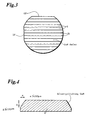
- Fig.2 shows an example of a wafer having notches N 1 and N2.
- N1 N2 in depth. If the depths of the notches N1 and N2 were more than or equal to 10mm and the angles of the notches N1 and N2 were more than or equal to 120 degrees, effective area of products (wafers) would be too narrow. When the depths and angles of the notches N1 and N2 were less than or equal to 2mm and 30 degrees respectively, the notches would be indiscernible.
- Bevel denotes a blunt inclination of an edge of a wafer which is caused by grinding, lapping and polishing. Elastic deformation of a polishing cloth wears out a sharp peripheral edge into a blunt slant and lowers the peripheral edge.
- the size of a bevel is represented by two components (e) and (g). One is a horizontal (width) component (e). The other is a vertical (depth) component (g).
- the bevel is an obstacle to devices made on the wafer by photolithography, since the surface is not flat at the periphery. Bevels are invited by a plurality of causes in the course of the surface processing (grinding, lapping and polishing).
- polishing is a collective concept including grinding and lapping.
- One is a single-surface polishing machine, which polishes only one surface of wafers.
- the other is a both-surface polishing machine, which polishes both surfaces at a stroke.
- This invention is related to an improvement of the single-surface polishing.
- the single surface polishing requires an operator to paste an object wafer to a polishing plate.
- a hot-melting type adhesive is employed for pasting a wafer to a polishing plate.
- the hot-melting type adhesive means such an adhesive that is softened by heating and is solidified by cooling.
- a wafer is stuck to a polishing plate by heating the plate, rubbing the plate with the hot-melting type adhesive, pasting a wafer on the adhesive-painted plate and cooling the plate.
- the hot-melting type adhesive is sometimes called a thermoplastic wax.
- the thermoplastic wax includes paraffine as a main component.
- the wax is heated up and molten at a temperature of Tm+20°C to Tm+50°C, where Tm is a softening temperature of the wax, and Tm+20°C is a temperature of Tm plus 20°C.
- Wax is actually painted on a bottom surface of a polishing plate by heating the plate up to a temperature between Tm+20°C and Tm+50°C and rubbing the hot plate with a solid wax by hand or painting a liquidized wax with brush. Wax is molten and is extended on the plate. When the wax is heated at a temperature of Tm+20°C or below, adhesion of the wax is insufficient.
- the thickness of the wax sandwiched between the polishing plate and the wafer should be 0.5 ⁇ m to 10 ⁇ m. A more suitable range of the wax thickness is 1 ⁇ m to 5 ⁇ m.
- An operator paints the polishing plate with the heated, softened wax by a brush or sprays liquidized wax on the polishing plate. The operator pastes wafers to the polishing plate by pushing the wafers on the wax coated plate. Pushing sometimes causes deformation of wafers due to air bubbles remaining. It is preferable to make a vacuum and eliminate air bubbles from the wax for suppressing the wafers from deforming. The reason why the wafers are glued to the polishing plate with the wax is that the wax painting is feasible for operation and the wax is excellent in adhesion strength.
- Inter-wafer fluctuation of the wax thickness among different wafers stuck to the same polishing plate should be less than or equal to 7 ⁇ m.
- a preferable range of the inter-wafer fluctuation of the wax thickness is 1 ⁇ m to 5 ⁇ m.
- the polished wafers have differences in thickness.
- a wax thickness fluctuation more than or equal to 7 ⁇ m should be forbidden, because the over 7 ⁇ m wax fluctuation causes serious fluctuation of wafer thicknesses.
- Distribution of wax thicknesses can be measured by a dial guage.
- the dial guage is a device of measuring the thickness of an object. When the initial distribution of wafer thicknesses has been measured, the wax thickness distribution can be obtained by the measurement with the dial guage.
- In-wafer fluctuation of the wax thickness within a wafer should be 5 ⁇ m or below.
- the in-wafer wax thickness fluctuation should be 3 ⁇ m or less.
- the wax thickness fluctuation is transcribed to the thickness fluctuation of the wafers after grinding, lapping and polishing.
- the wax thickness fluctuation of more than 5 ⁇ m induces large wafer thickness fluctuation and a large TTV (Total Thickness Variation) after grinding, lapping and polishing.
- a wafer after grinding is called a "postgrind” wafer.
- a wafer after lapping is called a "postlap” wafer hereafter.
- a wafer after polishing is called a "postpolish” wafer.
- a postpolish wafer is called a "mirror wafer", since the polished surface is flat and smooth like a mirror.
- More than 5 ⁇ m wax thickness fluctuation inhibits photolithography from depicting a correct pattern on the postpolish wafer.
- the postpolish wafers are removed from the polishing plate by heating the polishing plate, melting the wax and separating the wafers from the polishing plate. Otherwise, the postpolish wafers are separated by a sharp blade from the polishing plate.
- Another method for separation is to solve the wax with isopropyl alcohol or other organic solvents and to peel the wafers off the polishing plate.
- the direction of OFs or notches of wafers glued on a polishing plate is important.
- the OF (or notch) direction is a main problem of the surface planar processes of the present invention. When two flats or two notches are assigned, the larger flat or the larger notch is taken into consideration hereafter.
- the OF (or notch) direction has a great influence upon the result of the surface planar processes (grinding, lapping and polishing). If a wafer has an OF and an IF, the larger OF should be taken into account for determining the wafer direction on the plate.
- Fig.5 denotes a bottom view of a polishing plate 6 and wafers W1, W2, W3 and W4 glued on the polishing plate 6.
- Directions are defined with the rotation direction (arrow) of the polishing plate 6.
- forward angular direction in which the plate 6 runs
- backward b
- a centripetal radial direction from a wafer toward the plate center is named inward (u).
- a centrifugal radial direction from the plate center toward wafers is named outward (s).
- the result of surface planar processing depends upon the OF direction on the plate. In Fig.5, all the four wafers have OFs facing outward (s). This is the worst direction of OFs.
- OF-outward facing incurs bad results.
- This invention denies the outward facing OF.
- This invention favors inward (u), backward (b) and forward (f).
- a wafer has two flats (OF, IF) or two notches (N1, N2), both marks should not face outward (s).
- Wafer surface planar processing includes grinding, lapping and polishing. The three processes should be discriminated.
- Grinding, lapping and polishing are three different processes for wafer surface planar processing. Hitherto sometimes the word "polishing" is used as a collective concept for representing three different processes. Grinding is a step of roughly rubbing wafer surfaces with gross fixed whetting granules. Grinding eliminates large ruggedness, produces a flatter wafer surface and reduces a wafer thickness into a predetermined scope of thickness. Grinding is fastest in the speed of reducing a wafer thickness.
- Lapping employs either free whetting granules or fixed whetting granules.
- the granules of lapping are smaller than the whetting granules of grinding. Lapping further reduces surface ruggedness and eliminates grinding-induced degenerated superficial layers.
- Polishing which uses free whetting granules, is the final step of the planar processing steps. Polishing aims at decreasing surface roughness and removing grind/lapping-induced degenerated superficial layers.
- a polishing machine processes wafers glued on the polishing plate by supplying the wafers with a polishing liquid, rubbing the surfaces of the wafers with a whetting cloth and polishing the surfaces with fine free granules. Free granules are exchanged from larger sized granules via medium sized granules to fine sized granules at several steps. Surface evenness of wafers is increased step by step.
- OF-outward facing (s) of the wafers W1, W2, W3 and W4 is bad.
- the OF-outward facing (s) induces cracks, deep scars and damage on the wafers in the grinding step.
- the OF-outward facing (s) causes bruises and increase roughness on the wafers in the lapping step.
- the OF-outward facing (s) invites an increment of surface roughness and deep bevels (blunt edge slanting) on the wafers in the polishing step.
- wafers should be pasted on the polishing plate in the directions in which the orientation flats OF should not face outward (s).
- W5's OF faces forward (f).
- Forward (f) facing OF does not induce a large bevel.
- W6's OF faces inward (u).
- W7's OF faces inward (u).
- Inward (u) facing is also good.
- W8's OF faces backward (b).
- Backward (b) facing does not cause a big bevel. It is not necessary to equalize the OF-facing of all the wafers in a lot. It is important to paste wafers in the directions of facing the OFs backward (b), forward (f) or inward (u). Outward facing (s) is forbidden in the present invention.
- OF outward facing (s) of wafer directions induces a large bevel in polishing steps.
- the reason why the OF outward facing (s) invites a big bevel has not clearly been known yet by the inventors.
- OF outward facing (s) is assumed to reduce the effective diameter of pasted wafers due to the width of the orientation flats OF. Reduction of the effective contacting diameter will induce a sway motion in the polishing plate.
- OF outward facing (s) increases the pressure of the polishing cloth at the orientation flat (OF). Excess pressure will probably force grinding to cause scars and damage, lapping to increase surface roughness and polishing to cause bevels. Otherwise, OF outward facing (s) may induce disadvantageous flow in a polishing liquid or unfavorable deformation in a polishing cloth.
- the degree of OF-direction induced differences of qualities in grinding, lapping and polishing processes depends on the size of the OF.
- An OF length of more than or equal to 11mm (y ⁇ 11mm) invites conspicuous differences due to the difference of the OF-directions.
- FIG.7 shows an example of determining the pasting position of wafers.
- G is the center of a polishing plate 6.
- An edge circle of the polishing plate 6 is denoted by (q).
- the radius of the polishing plate 6 is denoted by (r).
- a half circle (v) (dotted line) is defined as a circle having the center G and a radius (r/2) which is a half of the plate radius (r).
- the half circle (v) is concentric with the plate edge circle (q) of the polishing plate 6. Centers of the wafers W9, W10 and W11 are denoted by C9, C10 and C11. The wafer centers should be out of the half circle (v). Namely the wafers should be allocated on the plate 6 under the conditions of GC9 > r/2, GC10>r/2 and GC11>r/2.
- a wafer circle (c) is defined as a circle passing the centers C9, C10 and C11 of the wafers W9, W10 and W11.
- the wafer circle (c) has a center at (G).
- the wafer circle (c) is concentric with the plate edge circle (q).
- the above conditions can be rewritten that the wafer circle (c) should be larger than the half circle (v).
- the outer wafer fixation condition stabilizes the rotation of polishing plate during the processing and improves the performance of the surface planar processing.
- An inner contact circle (j) (double dotted line) is defined as a circle being in contact with inner sides of the wafers W9, W10, and W11.
- the radius of a wafer is denoted by "w”.
- the diameter of the inner contact circle (j) is denoted by J.
- the other restriction is that the diameter J of the inner contact circle (j) should be larger than or equal to a length which is 0.35 times as long as the wafer diameter 2w. Namely J ⁇ 0.7w should be maintained. More favorably, the diameter J of the inner contact circle (j) should be longer than or equal to another length which is 0.4 times as long as the wafer diameter 2w.
- the more favorable condition is J ⁇ 0.8w. If the inner contact circle (j) were too narrow, the flow of a polishing liquid would be stagnated within the inner contact circle (j). Non-uniform flow of the polishing liquid would induce non-uniform grinding, lapping and polishing in the wafers. Thus the above inner restriction J ⁇ 0.7w (more favorably J ⁇ 0.8w) is imposed upon the position of the inner sides of the wafers on the polishing plate.
- an outer limit of the wafer pasting positions is given by the following consideration. As shown in Fig.7, the outer margin (p) between outermost sides of wafers and the plate edge (q) should be more than or equal to 1mm (p ⁇ 1mm).
- An outer contact circle (k), which is in contact with outer sides of wafers W9, W10 and W11, is depicted as a double-dotted circle in Fig.7. K denotes a diameter of the outer contact circle(k) (p r-K/2). The above means K/2 + 1mm ⁇ r. If the outer side of wafers were too close to the plate edge (q), the supply of a polishing liquid to the outer side of wafers would be insufficient and the outer sides would not be fully polished.
- the wafers should be pasted at inner points which are distanced from the plate edge (q) by at least 1mm. On the contrary, if wafers were stuck at too inner points, the previous inner contact circle (j) condition would not be satisfied.
- the margin (p) should have a preferable range of 3mm ⁇ p ⁇ 8mm.
- FIG.8 shows an example of two concentric circle allocation of wafers on a polishing plate.
- An inner wafer circle with a radius M and an outer wafer circle with a radius N are assumed concentrically on the polishing plate.
- Wafers W12, W 13, W14, W 15 and W16 are stuck along the inner wafer circle to the polishing plate with an equal distance M to the center.
- Wafers W17, W 18, W19, W20 and W21 are stuck along the outer wafer circle to the polishing plate with an equal distance N to the center.
- the inner circle group wafers should not align with the outer circle group wafers in radial directions.
- the inner circle group wafer W13 should be laid on a bisector of a top angle of an isosceles triangle which is formed by connecting centers of the neighboring outer circle wafers W21 and W17 to the plate center G. W13 is pasted on a bisector of ⁇ W21GW17 in Fig.8. The same relation should be maintained among other sets of the inner/outer group wafers.
- Such an allocation can equalize gaps between neighboring wafers. Uniform distribution of gaps forms uniform flow of polishing liquids on the polishing cloths. Uniform distribution of wafers equalizes the pressure acting on the wafers from the polishing cloth. Uniform pressure and uniform liquid flow bring stable rotation and low vibration of the polishing plate and the polishing turntable.
- This invention is available for groups 3 nitride wafers with uniform property without inner structure. In addition to the uniform wafers, this invention is also applicable to groups 3 nitride wafers with non-uniform property with inner structure.
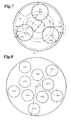
- This invention allows object nitride wafers to have a stripe structure. Such a stripe structure is inherent to nitride wafers. There are neither stripe structure Si wafer nor stripe structure GaAs wafer.
- the stripe structure is a special structure which appears on group 3 nitride crystal substrates by a particular method.
- a striped wafer means an anisotropic wafer having repetitions of parallel parts extending in a direction. Parallel sets of a linear dislocation accumulating region having many dislocations and a linear low defect single crystal region having a few dislocations align in the direction vertical to the extension.
- the facet-growth method enables the inventors to produce a freestanding low dislocation density GaN substrate wafer with a 50mm diameter.
- the facet-growth method is a novel method of making a rugged, facetted surface of growing film, growing the film with the facetted surface in vapor phase and maintaining the facetted surface till the end.
- a stripe mask or dot mask is formed on an undersubstrate.
- a nitride film is grown on the mask-carrying undersubstrate in vapor phase.
- Plenty of pits or valleys composed of facets are produced on the growing surface due to the mask.
- An orientation flat (OF) or a notch is made at a point on a circle edge of a group 3 nitride circular wafer for indicating orientation.
- the present invention pastes group 3 nitride wafers with a thermoplastic wax of a thickness less than or equal to 10 ⁇ m on a polishing plate with OFs (or notches) facing forward (f), inward (u) or backward (b) with regard to the rotation direction.
- This invention can make mirror wafers with low surface roughness and small bevels.
- the present invention enables the surface planar wafers to make epitaxial layers endowed with excellent crystallography and morphology and to make devices excellent in quality and yield.
- a polishing plate of an alumina (Al 2 O 3 ) disc with a 135mm diameter and a 30mm thickness is prepared.
- Sample wafers of grinding, lapping and polishing are HVPE as-grown GaN circular wafers with a 50mm diameter and a 0.5mm thickness.
- An as-grown GaN ingot is obtained by growing a GaN crystal on a GaAs undersubstrate and eliminating the GaAs undersubstrate.
- a plurality of as-grown GaN substrate wafers are produced by slicing the GaN ingot by a wire-saw.
- Each as-grown wafer has an orientation flat (OF) of a 16mm length.
- the central angle (T) of OF is 18 degrees.
- the eliminated width h for OF is 0.6mm.
- Each sample is a set of three as-grown wafers with an OF.
- Each Sample consists of three wafers. All the three wafers belonging to the same Sample are glued on the plate in the same facing u, f, b or s.
- the wax thickness distribution is calculated by measuring the wax thickness ⁇ of the wafers.
- An in-wafer wax distribution is the maximum of the differences ( ⁇ max - ⁇ min ) by subtracting the minimum wax thickness ( ⁇ min ) from the maximum wax thickness ( ⁇ max ) within each wafer glued on the plate.
- Samples 1, 2, 3 and 4 have in-wafer wax distributions of 3 ⁇ m, 3 ⁇ m, 2 ⁇ m and 2 ⁇ m respectively.
- An inter-wafer wax distribution is a difference ( ⁇ max - ⁇ min ) by subtracting the minimum wax thickness ( ⁇ min ) from the maximum wax thickness ( ⁇ max ) within all the wafers glued to the same plate.
- Samples 1, 2, 3 and 4 have inter-wafer wax distributions of 5 ⁇ m, 5 ⁇ m, 4 ⁇ m and 3 ⁇ m respectively.
- Samples 1, 2, 3 and 4 each of which consists of three wafers glued on a polishing plate, are ground, lapped and polished.
- a diamond whetting turntable which has fixed diamond whetting granules grinds the Samples.
- a metallic whetting turntable which has a flat metallic surface, laps the Samples with supplying a polishing liquid including diamond free whetting granules.
- a resin-polishing pad carrying turntable polishes the Samples with supplying another polishing liquid including free colloidal silica granules.
- a photointerference roughness tester examines surface roughness Rms of the postlap GaN wafers.
- a "postlap" wafer means a wafer which has experienced the lapping step.
- Five points are employed for examining Rms. Five examination points correspond to a center and four corners of an imaginary square having a center coinciding with the center of the wafer. Ranges of measured Rms at the five examination points are listed on Table 1. Table 1, line 6 denotes the ranges of Rms measured at five points on postlap Samples 1-4.
- Bevels of the postlap GaN wafers are measured.
- a bevel means an inclining round edge caused by polishing. Since photolithography depicts patterns on a wafer by light, it is ideal that the wafer should be flat till the peripheral edge. Edge bevels will cause deformation of patterns at the periphery of the wafer.
- Bevel is estimated by a horizontal width A, which is a vertical projection of the bevel on a horizontal plane, and by a vertical depth B, which is a horizontal projection on a vertical plane.
- the size of a bevel is expressed by a bevel width A and a bevel depth B.
- Fig.4 the edge slants are bevels.
- the horizontal width A is e.
- the vertical depth B is g.
- Postlapping bevel widths A of Samples 1, 2, 3 and 4 are all less than 10 ⁇ m, as shown in Table 1.
- the postlapping bevel depths B are also less than 10 ⁇ m.
- the above relates to the postlap wafers which have been lapped but have not been polished yet. Then the lapped GaN wafers are polished into mirror wafers.
- postpolish (mirror) wafers are described.
- Surface roughness Rms of the postpolish wafers is measured at five points, one center point and four peripheral points. The five examination spots correspond to a center and four corners of a square supposed on the wafer.
- Measured roughness of the postpolish Sample 1 is Rms 1.2nm to Rms 1.5nm at the five points, as listed in Table 1.
- Sample 4 is the largest also in four Samples 1-4 with regard to the postpolish roughness.
- Polishing enlarges bevels because elastic resin pads press the surfaces of wafers and deformed pads wear out the edges of wafers.
- Postpolish bevels of the wafers of Samples 1-4 after polishing are measured.
- Sample 1 shows a 140 ⁇ m postpolish bevel width A and a 43 ⁇ m postpolish bevel depth B.
- Sample 2 shows a 170 ⁇ m postpolish bevel width A and a 72 ⁇ m postpolish bevel depth B.
- Sample 3 denotes a 90 ⁇ m postpolish bevel width A and a 30 ⁇ m postpolish bevel depth B.
- Sample 4 shows a 360 ⁇ m postpolish bevel width A and a 120 ⁇ m postpolish bevel depth B.
- Sample 4 has a large vertical bevel B and horizontal bevel A.
- Sample 4 has wafers having outward (s) facing OFs. Large surface roughness and big bevel accompany the wafers with outward (s) facing OFs on the polishing plate.
- Wafer thickness fluctuation is defined as a difference of thicknesses of wafers glued on a polishing plate.
- the wafer thickness fluctuation is a difference by subtracing the minimum wafer thickness from the maximum wafer thickness. Large wafer thickness fluctuation of the postpolished wafers indicates poor polishing.
- Sample 1, 2, 3 and 4 show wafer thickness fluctuation of 7 ⁇ m, 8 ⁇ m, 6 ⁇ m and 6 ⁇ m respectively.
- the standard thickness of the wafers is 500 ⁇ m.
- LEDs Light emitting diodes
- n-GaN layer an InGaN layer and a p-GaN layer on the mirror wafers of Samples 1-4.
- the LEDs are examined and are classified into approved products and rejects.
- the yield which is a ratio of approved/total products, is shown on the Table 1 for Sample 1-4.
- a 50 mm diameter wafer can make about 2000 LEDs with a 400 ⁇ m square.
- LED yields of Samples 1-4 are 60%, 52%, 68% and 38%.
- Sample 4 which is annoyed with a large bevel and large postpolish surface roughness Rms, has a drawback of a low LED yield.
- Embodiment 2 employs a polishing plate of an alumina (Al 2 O 3 ) disc with a 155mm diameter and a 30mm thickness.
- Object GaN wafers of grinding, lapping and polishing processes are sets of stripe structure HVPE-as-grown GaN wafers with a 50mm diameter and a 0.5mm thickness.
- the stripe structure means a non-uniform GaN crystal having reciprocally alternating sets of parallel low density single crystal regions and parallel defect accumulating regions.
- the stripe structure GaN wafers have been made by preparing a GaAs undersubstrate, producing a stripe mask on the GaAs undersubstrate, growing a GaN film crystal on the stripe-masked undersubstrate by an HVPE method, producing facets and maintaining the facet till the end.
- HVPE-as-grown GaN/GaAs complex wafers are made.
- An as-grown GaN freestanding wafer is obtained by removing the GaAs undersubstrate and chamfering an edge.
- a tall GaN crystal is grown on a GaAs undersubstrate for a long time by the HVPE method
- a plurality of freestanding GaN wafers are made by vertically slicing the GaN ingot with a wire-saw into a plurality of as-grown GaN wafers.
- Five as-grown GaN wafers are chosen as a set of sample wafers for grinding, lapping and polishing at a lot.
- a notch is allotted to an edge of each GaN wafer for indicating orientation. The notch has a 5mm depth and a 60 degree angle.
- Five as-grown GaN wafers are glued with a thermoplastic solid wax on a polishing plate.
- the polishing plate is heated up to Tm+30°C, where Tm is the softening temperature.
- Tm is the softening temperature.
- Wax thickness distribution is examined by gluing wafers to a polishing plate, measuring thicknesses ( ⁇ ) of the wax layer at plenty of points aligning two-dimensionally on the wafers and calculating fluctuation of the wax thicknesses.
- In-wafer wax thickness fluctuation is defined as a difference ( ⁇ max - ⁇ min ) between the wax thickness maximum ( ⁇ max ) within a wafer and the wax thickness minimum ( ⁇ min ) within the same wafer.
- Samples 5, 6, 7, and 8 reveal 3 ⁇ m, 3 ⁇ m, 7 ⁇ m and 8 ⁇ m respectively of the in-wafer wax thickness fluctuation.
- Inter-wafer wax thickness distribution means the fluctuation of the wax thicknesses of a lot of the wafers glued on the same polishing plate.
- the inter-wafer is defined as a difference between the maximum wax thickness and the minimum wax thickness of the wafers stuck on a common polishing plate.
- Measured inter-wax thickness fluctuation is 5 ⁇ m, 5 ⁇ m, 9 ⁇ m and 11 ⁇ m for Samples 5, 6, 7 and 8
- Wafer thickness fluctuation denotes the fluctuation of the thicknesses of a wafer.
- the wafer thickness fluctuation is defined as a difference (d max -d min ) between the wafer thickness maximum (d max ) and the wafer thickness minimum (d min ).
- Wafer thickness fluctuation measured is 7 ⁇ m, 8 ⁇ m, 13 ⁇ m and 18 ⁇ m for Samples 5, 6, 7 and 8 respectively.
- Each sample consists of five wafers stuck to a polishing plate.
- Samples 5, 6, 7 and 8, which are sets of five wafers glued on the polishing plate, are ground, lapped and polished.
- the Samples 5-8 are ground by a diamond fixed granule whetting turntable.
- the Samples 5-8 ground are lapped by a metallic whetting turntable with supplying free diamond granules containing liquid.
- the Samples 5-8 lapped are polished by a resin-pad covered turntable with supplying a liquid including free colloidal silica granules.
- Surface roughness of postlap GaN wafers is measured by a photointerference roughness tester. Roughness is measured at five points which are a center and four corners of a square whose center coincides with the center of the postlap wafer. The range of the postlap roughness measured at the five points is listed on Table 2 for Samples 5, 6, 7 and 8.
- Sample 8 reveals the highest surface roughness of postlap wafers.
- the large wax thickness fluctuation may invite large postlap surface roughness.
- the lapped wafers of Samples 5-8 are polished into mirror wafers.
- Surface roughness of postpolish GaN wafers is measured by the same photointerference roughness tester. Roughness is measured at five points which are a center and four corners of a square whose center coincides with the center of the postpolish wafer. The ranges of the postpolish roughness measured at the five points are listed on Table 2 for Samples 5, 6, 7 and 8.
- Sample 8 reveals the highest surface roughness of postpolish wafers.
- the large wax thickness fluctuation may invite large postpolish surface roughness.
- Epitaxial wafers are produced by epitaxially grow n-type GaN films, InGaN films and p-type GaN films on the polished GaN wafers.
- P-electrodes and n-electrodes are formed on the epitaxial wafers.
- LEDs are produced by dividing the processed wafers into chips and packaging the chips. Light power and spectrum of LEDs are examined by supplying current, making LEDs lighten and testing emission power and emission spectrum. The LEDs are judged to be approved products or rejects. Yields, which are defined as a ratio of the number of the approved products to the total number, are shown every Sample.
- a 50mm diameter wafer can produce about 2000 LED chips of a 400 ⁇ m square.
- the yields are listed on Table 2.
- the yields of Samples 5, 6, 7 and 8 are 60%, 52%, 32% and 17 %.
- Large fluctuation of wax thickness invites large wafer thickness fluctuation in Samples 7 and 8.
- Big wax/wafer thickness fluctuation causes large postlap and postpolish surface roughness Rms in Samples 7 and 8.
- Samples 7 and 8 are annoyed with low yield which results from the large postpolish roughness Rms and big wafer thickness fluctuation.
- Comparison of Samples 5, 6, 7 and 8 teaches us that allowable in-wafer wax thickness fluctuation is less than 7 ⁇ m and preferable wax thickness fluctuation is less than or equal to 5 ⁇ m.
Landscapes
- Engineering & Computer Science (AREA)
- Mechanical Engineering (AREA)
- Mechanical Treatment Of Semiconductor (AREA)
- Finish Polishing, Edge Sharpening, And Grinding By Specific Grinding Devices (AREA)
Applications Claiming Priority (2)
| Application Number | Priority Date | Filing Date | Title |
|---|---|---|---|
| JP2006191000 | 2006-07-12 | ||
| JP2006337678A JP2008042157A (ja) | 2006-07-12 | 2006-12-15 | 3族窒化物基板の製造方法、および3族窒化物基板 |
Publications (1)
| Publication Number | Publication Date |
|---|---|
| EP1879222A2 true EP1879222A2 (de) | 2008-01-16 |
Family
ID=38657940
Family Applications (1)
| Application Number | Title | Priority Date | Filing Date |
|---|---|---|---|
| EP07008346A Withdrawn EP1879222A2 (de) | 2006-07-12 | 2007-04-24 | Verfahren zur Herstellung von Gruppe-3-Nitridsubstrat-Wafern und Gruppe-3-Nitridsubstrat-Wafer |
Country Status (5)
| Country | Link |
|---|---|
| US (1) | US7662239B2 (de) |
| EP (1) | EP1879222A2 (de) |
| JP (1) | JP2008042157A (de) |
| KR (1) | KR20080006446A (de) |
| TW (1) | TWI336908B (de) |
Families Citing this family (10)
| Publication number | Priority date | Publication date | Assignee | Title |
|---|---|---|---|---|
| JP2008042157A (ja) * | 2006-07-12 | 2008-02-21 | Sumitomo Electric Ind Ltd | 3族窒化物基板の製造方法、および3族窒化物基板 |
| JP2009272380A (ja) * | 2008-05-01 | 2009-11-19 | Sumitomo Electric Ind Ltd | Iii族窒化物結晶およびその表面処理方法、iii族窒化物積層体およびその製造方法、ならびにiii族窒化物半導体デバイスおよびその製造方法 |
| JP5233936B2 (ja) * | 2009-09-24 | 2013-07-10 | 住友電気工業株式会社 | 窒化物半導体基板 |
| US9946730B2 (en) * | 2011-11-04 | 2018-04-17 | Ebay Inc. | System and method for onboarding an item collection |
| US8471366B2 (en) | 2011-11-30 | 2013-06-25 | Sumitomo Electric Industries, Ltd. | Nitride semiconductor substrate |
| JP2013138259A (ja) * | 2013-03-28 | 2013-07-11 | Sumitomo Electric Ind Ltd | 窒化物半導体基板 |
| JP5846223B2 (ja) * | 2014-01-21 | 2016-01-20 | 住友電気工業株式会社 | 基板および発光素子 |
| JP6063436B2 (ja) * | 2014-12-18 | 2017-01-18 | Dowaエレクトロニクス株式会社 | ウェハ群、ウェハの製造装置、およびウェハの製造方法 |
| JP6390684B2 (ja) * | 2016-10-07 | 2018-09-19 | トヨタ自動車株式会社 | SiC単結晶の製造方法 |
| JP7162559B2 (ja) * | 2019-03-27 | 2022-10-28 | 株式会社ノリタケカンパニーリミテド | ウェハ研磨方法及びウェハ研磨装置 |
Family Cites Families (8)
| Publication number | Priority date | Publication date | Assignee | Title |
|---|---|---|---|---|
| JP2002222746A (ja) | 2001-01-23 | 2002-08-09 | Matsushita Electric Ind Co Ltd | 窒化物半導体ウェーハ及びその製造方法 |
| JP2002222785A (ja) | 2001-01-24 | 2002-08-09 | Dowa Mining Co Ltd | 半導体ウエハおよびその研磨方法 |
| US6488767B1 (en) | 2001-06-08 | 2002-12-03 | Advanced Technology Materials, Inc. | High surface quality GaN wafer and method of fabricating same |
| US6791120B2 (en) * | 2002-03-26 | 2004-09-14 | Sanyo Electric Co., Ltd. | Nitride-based semiconductor device and method of fabricating the same |
| JP2004165360A (ja) | 2002-11-12 | 2004-06-10 | Hitachi Cable Ltd | 半導体ウェハの研磨方法 |
| JP3534115B1 (ja) * | 2003-04-02 | 2004-06-07 | 住友電気工業株式会社 | エッジ研磨した窒化物半導体基板とエッジ研磨したGaN自立基板及び窒化物半導体基板のエッジ加工方法 |
| JP4322035B2 (ja) | 2003-04-03 | 2009-08-26 | ニッタ・ハース株式会社 | 半導体基板用研磨組成物及びこれを用いた半導体基板研磨方法 |
| JP2008042157A (ja) * | 2006-07-12 | 2008-02-21 | Sumitomo Electric Ind Ltd | 3族窒化物基板の製造方法、および3族窒化物基板 |
-
2006
- 2006-12-15 JP JP2006337678A patent/JP2008042157A/ja not_active Withdrawn
-
2007
- 2007-04-24 EP EP07008346A patent/EP1879222A2/de not_active Withdrawn
- 2007-04-24 TW TW096114452A patent/TWI336908B/zh not_active IP Right Cessation
- 2007-05-04 KR KR1020070043610A patent/KR20080006446A/ko not_active Ceased
- 2007-07-11 US US11/822,903 patent/US7662239B2/en not_active Expired - Fee Related
Also Published As
| Publication number | Publication date |
|---|---|
| HK1113859A1 (zh) | 2008-10-17 |
| TWI336908B (en) | 2011-02-01 |
| KR20080006446A (ko) | 2008-01-16 |
| TW200805474A (en) | 2008-01-16 |
| US7662239B2 (en) | 2010-02-16 |
| JP2008042157A (ja) | 2008-02-21 |
| US20080014756A1 (en) | 2008-01-17 |
Similar Documents
| Publication | Publication Date | Title |
|---|---|---|
| EP1879222A2 (de) | Verfahren zur Herstellung von Gruppe-3-Nitridsubstrat-Wafern und Gruppe-3-Nitridsubstrat-Wafer | |
| US11826846B2 (en) | Laser-assisted method for parting crystalline material | |
| US11911842B2 (en) | Laser-assisted method for parting crystalline material | |
| US6875082B2 (en) | Nitride semiconductor wafer and method of processing nitride semiconductor wafer | |
| CN104769704B (zh) | 半导体晶片的加工方法 | |
| CN100485879C (zh) | 制造ⅲ族氮化物衬底晶片的方法和ⅲ族氮化物衬底晶片 | |
| US9324558B2 (en) | Machining process for semiconductor wafer | |
| US20140234568A1 (en) | Sapphire substrate | |
| WO2008083073A1 (en) | Sapphire substrates and methods of making same | |
| WO2008083071A1 (en) | Method of grinding a sapphire substrate | |
| KR20080022048A (ko) | 3족 질화물 기판의 제조 방법, 3족 질화물 기판,에피텍셜층이 부착된 3족 질화물 기판, 3족 질화물디바이스, 에피텍셜층이 부착된 3족 질화물 기판의 제조방법 및 3족 질화물 디바이스의 제조 방법 | |
| US20180297168A1 (en) | Semiconductor wafer processing method | |
| JP2003229392A (ja) | シリコンウエーハの製造方法及びシリコンウエーハ並びにsoiウエーハ | |
| KR20200104909A (ko) | 웨이퍼의 제조 방법 | |
| US20120028439A1 (en) | Semiconductor And Solar Wafers And Method For Processing Same | |
| CN116352899A (zh) | 一种碳化硅晶体切割头尾片的处理方法 | |
| EP4224514A1 (de) | Epitaxiales sic-substrat und verfahren zur herstellung desselben | |
| HK1113859B (en) | Method of producing group 3 nitride substrate wafers and group 3 nitride substrate wafers | |
| JP2000068556A (ja) | 窒化物半導体ウエハの研削装置及び研削方法 | |
| CN118752386A (zh) | 一种氧化镓单晶衬底抛光片的划片保护层结构及其划片方法 | |
| KR20110042438A (ko) | 사파이어 웨이퍼의 연마방법 |
Legal Events
| Date | Code | Title | Description |
|---|---|---|---|
| PUAI | Public reference made under article 153(3) epc to a published international application that has entered the european phase |
Free format text: ORIGINAL CODE: 0009012 |
|
| AK | Designated contracting states |
Kind code of ref document: A2 Designated state(s): AT BE BG CH CY CZ DE DK EE ES FI FR GB GR HU IE IS IT LI LT LU LV MC MT NL PL PT RO SE SI SK TR |
|
| AX | Request for extension of the european patent |
Extension state: AL BA HR MK YU |
|
| RIN1 | Information on inventor provided before grant (corrected) |
Inventor name: NAKAHATA, SEIJI Inventor name: IRIKURA, MASATO Inventor name: ISHIBASHI, KEIJI |
|
| STAA | Information on the status of an ep patent application or granted ep patent |
Free format text: STATUS: THE APPLICATION IS DEEMED TO BE WITHDRAWN |
|
| 18D | Application deemed to be withdrawn |
Effective date: 20111031 |