EP1879272A1 - Laser mit photonischem kristall - Google Patents
Laser mit photonischem kristall Download PDFInfo
- Publication number
- EP1879272A1 EP1879272A1 EP05737342A EP05737342A EP1879272A1 EP 1879272 A1 EP1879272 A1 EP 1879272A1 EP 05737342 A EP05737342 A EP 05737342A EP 05737342 A EP05737342 A EP 05737342A EP 1879272 A1 EP1879272 A1 EP 1879272A1
- Authority
- EP
- European Patent Office
- Prior art keywords
- photonic crystal
- light
- laser
- upper electrodes
- electrodes
- Prior art date
- Legal status (The legal status is an assumption and is not a legal conclusion. Google has not performed a legal analysis and makes no representation as to the accuracy of the status listed.)
- Withdrawn
Links
- 239000004038 photonic crystal Substances 0.000 title claims abstract description 97
- 230000000737 periodic effect Effects 0.000 claims description 15
- 238000002347 injection Methods 0.000 claims description 6
- 239000007924 injection Substances 0.000 claims description 6
- 239000012780 transparent material Substances 0.000 claims description 2
- 230000007246 mechanism Effects 0.000 abstract description 5
- 239000010410 layer Substances 0.000 description 53
- 108091008695 photoreceptors Proteins 0.000 description 16
- 238000010276 construction Methods 0.000 description 12
- 125000006850 spacer group Chemical group 0.000 description 7
- JBRZTFJDHDCESZ-UHFFFAOYSA-N AsGa Chemical compound [As]#[Ga] JBRZTFJDHDCESZ-UHFFFAOYSA-N 0.000 description 6
- 238000000034 method Methods 0.000 description 6
- 229910001218 Gallium arsenide Inorganic materials 0.000 description 5
- 239000000463 material Substances 0.000 description 5
- 230000010355 oscillation Effects 0.000 description 5
- 239000000969 carrier Substances 0.000 description 4
- 238000005253 cladding Methods 0.000 description 4
- FTWRSWRBSVXQPI-UHFFFAOYSA-N alumanylidynearsane;gallanylidynearsane Chemical compound [As]#[Al].[As]#[Ga] FTWRSWRBSVXQPI-UHFFFAOYSA-N 0.000 description 3
- 239000013078 crystal Substances 0.000 description 3
- 238000010586 diagram Methods 0.000 description 3
- PCHJSUWPFVWCPO-UHFFFAOYSA-N gold Chemical compound [Au] PCHJSUWPFVWCPO-UHFFFAOYSA-N 0.000 description 3
- 229910052737 gold Inorganic materials 0.000 description 3
- 239000010931 gold Substances 0.000 description 3
- 239000004065 semiconductor Substances 0.000 description 3
- 239000000758 substrate Substances 0.000 description 3
- 229910000530 Gallium indium arsenide Inorganic materials 0.000 description 2
- PXHVJJICTQNCMI-UHFFFAOYSA-N Nickel Chemical compound [Ni] PXHVJJICTQNCMI-UHFFFAOYSA-N 0.000 description 2
- KXNLCSXBJCPWGL-UHFFFAOYSA-N [Ga].[As].[In] Chemical compound [Ga].[As].[In] KXNLCSXBJCPWGL-UHFFFAOYSA-N 0.000 description 2
- 238000000151 deposition Methods 0.000 description 2
- 238000000605 extraction Methods 0.000 description 2
- XLOMVQKBTHCTTD-UHFFFAOYSA-N Zinc monoxide Chemical compound [Zn]=O XLOMVQKBTHCTTD-UHFFFAOYSA-N 0.000 description 1
- 230000001174 ascending effect Effects 0.000 description 1
- 239000003086 colorant Substances 0.000 description 1
- 238000007796 conventional method Methods 0.000 description 1
- 230000000694 effects Effects 0.000 description 1
- 229910052732 germanium Inorganic materials 0.000 description 1
- GNPVGFCGXDBREM-UHFFFAOYSA-N germanium atom Chemical compound [Ge] GNPVGFCGXDBREM-UHFFFAOYSA-N 0.000 description 1
- 229910052759 nickel Inorganic materials 0.000 description 1
- 230000005855 radiation Effects 0.000 description 1
- 239000002356 single layer Substances 0.000 description 1
Images
Classifications
-
- B—PERFORMING OPERATIONS; TRANSPORTING
- B41—PRINTING; LINING MACHINES; TYPEWRITERS; STAMPS
- B41J—TYPEWRITERS; SELECTIVE PRINTING MECHANISMS, i.e. MECHANISMS PRINTING OTHERWISE THAN FROM A FORME; CORRECTION OF TYPOGRAPHICAL ERRORS
- B41J2/00—Typewriters or selective printing mechanisms characterised by the printing or marking process for which they are designed
- B41J2/435—Typewriters or selective printing mechanisms characterised by the printing or marking process for which they are designed characterised by selective application of radiation to a printing material or impression-transfer material
- B41J2/447—Typewriters or selective printing mechanisms characterised by the printing or marking process for which they are designed characterised by selective application of radiation to a printing material or impression-transfer material using arrays of radiation sources
- B41J2/45—Typewriters or selective printing mechanisms characterised by the printing or marking process for which they are designed characterised by selective application of radiation to a printing material or impression-transfer material using arrays of radiation sources using light-emitting diode [LED] or laser arrays
-
- H—ELECTRICITY
- H01—ELECTRIC ELEMENTS
- H01S—DEVICES USING THE PROCESS OF LIGHT AMPLIFICATION BY STIMULATED EMISSION OF RADIATION [LASER] TO AMPLIFY OR GENERATE LIGHT; DEVICES USING STIMULATED EMISSION OF ELECTROMAGNETIC RADIATION IN WAVE RANGES OTHER THAN OPTICAL
- H01S5/00—Semiconductor lasers
- H01S5/04—Processes or apparatus for excitation, e.g. pumping, e.g. by electron beams
- H01S5/042—Electrical excitation ; Circuits therefor
- H01S5/0425—Electrodes, e.g. characterised by the structure
- H01S5/04252—Electrodes, e.g. characterised by the structure characterised by the material
- H01S5/04253—Electrodes, e.g. characterised by the structure characterised by the material having specific optical properties, e.g. transparent electrodes
-
- H—ELECTRICITY
- H01—ELECTRIC ELEMENTS
- H01S—DEVICES USING THE PROCESS OF LIGHT AMPLIFICATION BY STIMULATED EMISSION OF RADIATION [LASER] TO AMPLIFY OR GENERATE LIGHT; DEVICES USING STIMULATED EMISSION OF ELECTROMAGNETIC RADIATION IN WAVE RANGES OTHER THAN OPTICAL
- H01S5/00—Semiconductor lasers
- H01S5/04—Processes or apparatus for excitation, e.g. pumping, e.g. by electron beams
- H01S5/042—Electrical excitation ; Circuits therefor
- H01S5/0425—Electrodes, e.g. characterised by the structure
- H01S5/04256—Electrodes, e.g. characterised by the structure characterised by the configuration
-
- H—ELECTRICITY
- H01—ELECTRIC ELEMENTS
- H01S—DEVICES USING THE PROCESS OF LIGHT AMPLIFICATION BY STIMULATED EMISSION OF RADIATION [LASER] TO AMPLIFY OR GENERATE LIGHT; DEVICES USING STIMULATED EMISSION OF ELECTROMAGNETIC RADIATION IN WAVE RANGES OTHER THAN OPTICAL
- H01S5/00—Semiconductor lasers
- H01S5/10—Construction or shape of the optical resonator, e.g. extended or external cavity, coupled cavities, bent-guide, varying width, thickness or composition of the active region
- H01S5/18—Surface-emitting [SE] lasers, e.g. having both horizontal and vertical cavities
- H01S5/185—Surface-emitting [SE] lasers, e.g. having both horizontal and vertical cavities having only horizontal cavities, e.g. horizontal cavity surface-emitting lasers [HCSEL]
-
- H—ELECTRICITY
- H01—ELECTRIC ELEMENTS
- H01S—DEVICES USING THE PROCESS OF LIGHT AMPLIFICATION BY STIMULATED EMISSION OF RADIATION [LASER] TO AMPLIFY OR GENERATE LIGHT; DEVICES USING STIMULATED EMISSION OF ELECTROMAGNETIC RADIATION IN WAVE RANGES OTHER THAN OPTICAL
- H01S2301/00—Functional characteristics
- H01S2301/18—Semiconductor lasers with special structural design for influencing the near- or far-field
-
- H—ELECTRICITY
- H01—ELECTRIC ELEMENTS
- H01S—DEVICES USING THE PROCESS OF LIGHT AMPLIFICATION BY STIMULATED EMISSION OF RADIATION [LASER] TO AMPLIFY OR GENERATE LIGHT; DEVICES USING STIMULATED EMISSION OF ELECTROMAGNETIC RADIATION IN WAVE RANGES OTHER THAN OPTICAL
- H01S5/00—Semiconductor lasers
- H01S5/04—Processes or apparatus for excitation, e.g. pumping, e.g. by electron beams
- H01S5/042—Electrical excitation ; Circuits therefor
- H01S5/0428—Electrical excitation ; Circuits therefor for applying pulses to the laser
-
- H—ELECTRICITY
- H01—ELECTRIC ELEMENTS
- H01S—DEVICES USING THE PROCESS OF LIGHT AMPLIFICATION BY STIMULATED EMISSION OF RADIATION [LASER] TO AMPLIFY OR GENERATE LIGHT; DEVICES USING STIMULATED EMISSION OF ELECTROMAGNETIC RADIATION IN WAVE RANGES OTHER THAN OPTICAL
- H01S5/00—Semiconductor lasers
- H01S5/06—Arrangements for controlling the laser output parameters, e.g. by operating on the active medium
- H01S5/062—Arrangements for controlling the laser output parameters, e.g. by operating on the active medium by varying the potential of the electrodes
- H01S5/06233—Controlling other output parameters than intensity or frequency
- H01S5/06243—Controlling other output parameters than intensity or frequency controlling the position or direction of the emitted beam
-
- H—ELECTRICITY
- H01—ELECTRIC ELEMENTS
- H01S—DEVICES USING THE PROCESS OF LIGHT AMPLIFICATION BY STIMULATED EMISSION OF RADIATION [LASER] TO AMPLIFY OR GENERATE LIGHT; DEVICES USING STIMULATED EMISSION OF ELECTROMAGNETIC RADIATION IN WAVE RANGES OTHER THAN OPTICAL
- H01S5/00—Semiconductor lasers
- H01S5/10—Construction or shape of the optical resonator, e.g. extended or external cavity, coupled cavities, bent-guide, varying width, thickness or composition of the active region
- H01S5/11—Comprising a photonic bandgap structure
Definitions
- the present invention relates to a laser element that can be preferably used for various kinds of devices such as laser printers, bar code readers or other devices where a laser light needs to be scanned, and a laser device.
- a laser light is scanned in order to print data or read data.
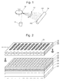
- Fig. 1 is a laser scanning device in conventional laser printers.
- a laser light emitted from a semiconductor laser 11 is reflected on a side surface of a rotating polygon mirror 12, and passes through an f- ⁇ lens 13 to irradiate a photoreceptor drum 14. While a laser light is irradiated onto one of the side surfaces of the polygon mirror 12, the irradiation point of the laser light (i.e. laser light spot) moves from one end 151 to the other end 152 of the photoreceptor drum 14 continuously due to the rotation of the polygon mirror 12. When the laser light spot reaches said the other end 152, the reflection of the laser light on the polygon mirror 12 is positioned exactly at an edge of the side surface of the polygon mirror.
- the reflection of the laser light is positioned at a beginning edge of the subsequent side surface, and thereby the laser light spot on the photoreceptor drum 14 returns to said one end 151.
- a laser light is thus irradiated on the photoreceptor drum 14 while being scanned repeatedly, during which the laser light is turned on/off, and characters and images are thus printed.
- the scanning speed of the laser light spot on the photoreceptor drum needs to be increased.
- the speed of the laser light spot scanned on the photoreceptor drum 14 is determined by the rotation speed of the polygon mirror.
- Patent Document 1 discloses a construction which further enhances the scanning speed by using a laser light source where a plurality of vertical cavity surface emitting lasers (VCSELs) are arranged in the form of an array. According to this construction, the scanning speed is enhanced by emitting laser lights from the plurality of the VCSELs simultaneously. However, it is difficult to make VCSELs to be capable of moving the beams, and a polygon mirror is inevitable in scanning. Another problem is that the output of a single mode VCSEL is limited to about 3 mW.
- VCSELs vertical cavity surface emitting lasers
- a photonic crystal is made of a dielectric body in which an artificial periodic structure is created.
- the periodic structure is created by providing the dielectric body with a periodic arrangement of areas whose refractive index differs from that of the dielectric body.
- the periodic structure causes a Bragg diffraction within the crystal and creates an energy band gap with respect to the energy of light.
- Patent Document 2 discloses a laser light source using a two-dimensional photonic crystal. This laser light source includes an active layer including a light-emitting material inserted between a pair of electrodes (or conductive semiconductor layers), and a two-dimensional photonic crystal located on an upper surface of the active layer.
- the two-dimensional photonic crystal is made of a plate member (or slab) whose refractive index is periodically distributed over a two-dimensional area.
- An injection of carriers from the electrodes generates light in the active layer, and the light is intensified by the diffraction due to the periodic structure of the two-dimensional photonic crystal, which causes a laser oscillation.
- the distance of a period of the periodic structure is consonant with the wavelength in the medium, light is emitted in the direction vertical to the slab surface.
- This laser light source produces light emission whose output power is larger than that of the VCSEL.
- Patent Document 1 Unexamined Japanese Patent Publication No. 2000-020995 (Paragraph [0012], Fig. 2)
- Patent Document 2 Unexamined Japanese Patent Publication No. 2000-332351 (Paragraphs [0037] to [0056], Fig. 1)
- One objective of the present invention is to provide a laser element and a laser device where beams of laser light of high output power can be scanned at a high speed without using mechanical scanning systems.
- a first aspect of a photonic crystal laser element according to the present invention that has been made to achieve the above-mentioned problem includes:
- a second aspect of the photonic crystal laser element according to the present invention includes:
- a photonic crystal laser device is provided with the above-described photonic crystal laser element, a voltage application means for applying a voltage between the upper electrode and the lower electrode, and a control means for controlling the on/off of the voltage applied to each of the plurality of the arranged upper electrodes or the lower electrodes.
- both layers and other layers can be arranged in an arbitrary direction as long as the arrangement order is as stated above.
- the photonic crystal laser element according to the present invention includes the active layer and the two-dimensional photonic crystal. This aspect is similar to that of the laser disclosed in Patent Document 2.
- the two-dimensional photonic crystal here does not need to be in direct contact with the active layer; it is possible to insert a spacer or other layers to obtain a sufficient feedback effect. Such a layer is inserted to adjust a distance between the active layer and the two-dimensional photonic crystal, so that size adjustments of a light-emitting area can be realized.
- An injection of electric charges causes the active layer to generate light of a predetermined wavelength.
- the active layer may use, for example, the same material as those conventionally used in Fabry-Perot laser light sources.
- the two-dimensional photonic crystal is generally made of a slab body provided with a large number of periodically arranged, same-shaped areas whose refractive index differs from that of the body material.
- the periodical structure is triangular, square, hexagonal lattice patterns or other patterns.
- the distance of a period is set to correspond to the wavelength of a light generated in the active layer. Although the periodic distance is generally set to match the wavelength of the generated light, there are cases where a laser oscillation is possible in other periodic distances (e.g. half of the wavelength).
- the upper electrodes and the lower electrode are provided so as to sandwitch the active layer and the two-dimensional photonic crystal. Other layers may be inserted between the active layer and the lower layer.
- the plurality of the upper electrodes are separately arranged on the upper side of the two-dimensional photonic crystal.
- the upper electrodes may be arranged linearly (or one-dimensionally), or may be arrange two-dimensionally in a square lattice pattern, a triangular lattice pattern or other patterns.
- Other layers may also be inserted between the two-dimensional crystal and the upper electrodes.
- the upper electrodes may be mounted onto a layer member arranged between two-dimensional photonic crystal and the upper electrodes.
- a plurality of lower electrodes may be provided on the lower side of the active layer so as to correspond to the upper electrodes, or a single lower electrode common to the plurality of the upper electrodes may be provided.
- Other layers may also be inserted between the lower electrode(s) and the active layer. It is desirable that the lower electrode(s) or the inserted layer reflects light so as to avoid a leakage of light generated in the active layer from the lower electrode side to the outside.
- a photonic crystal laser device is composed of the element thus constructed, and a voltage application means and a control means.
- the voltage application means is provided to apply a voltage between the upper electrodes and the lower electrode(s), where a usual DC power supply may be used.
- the control means is provided to control an on/off of the application voltage in each of the upper electrodes. The on/off timing in each of the upper electrodes may be appropriately determined in accordance with purposes of the photonic crystal laser as described in examples shown later.
- the photonic crystal laser element and the laser light source according to the present invention operations which are not observed in conventional lasers can be realized due to the arrangement that a plurality of upper electrodes are provided.
- the light-emitting areas can be switched by the control means which controls the on/off of the application voltage in each of the upper electrodes, and thereby beams of the laser light can be apparently shifted.
- the size (or diameter) of a light-emitting area around an upper electrode is d, and when a large number of upper electrodes are disposed by setting the distance therebetween to be smaller than d, and a voltage is simultaneously applied (or turned on) to a predetermined number of adjacently disposed upper electrodes, these upper electrodes as a whole creates one light-emitting area (i.e, broad light-emitting area).
- the broad light-emitting area can be shifted gradually or stepwise.
- the former method allows smooth movement of the light-emitting area
- the latter method allows a prompt movement of the light-emitting area. In either method, the light-emitting area is broad and thereby a laser light of high output power can be generated.
- the irradiation range of a laser light is only within the entire length (or entire width) of the element because the laser light is radiated from the light-emitting area in a substantially vertical direction. Accordingly, if irradiation into a broader range is required, a means for changing the direction of a laser light outputted around each of the upper electrodes (deflection means) is desirably provided on the upper electrodes.
- the deflection means includes a lens to cover the entire element, a prism provided in each elements, and the like.
- a plurality of lower electrodes instead of upper electrodes, may also be arranged.
- a single upper electrode common to the plurality of or the entire lower electrodes is sufficient.
- a voltage is applied between each of the lower electrodes and the upper electrode, a laser light is radiated from the upper electrode to the outside in a range straightly above a predetermined range around respective lower electrodes.
- the operation of the photonic crystal laser element and the laser device according to the second aspect is the same as that of the first aspect.
- the wavelength of the laser light can be tuned by providing different periodic structures depending on positions within the photonic crystal.
- the laser light can be scanned by turning on/off a voltage applied to the plurality of the arranged upper electrodes or lower electrodes without using mechanical scanning mechanisms.
- the scanning speed of the laser light is not limited by the speed of the mechanical scanning mechanisms, so that it can be larger than that of the conventional techniques.
- using the photonic crystal laser capable of emitting light in large output power allows a sufficient increase in the intensity of an obtained laser light.
- the photonic crystal laser of the present invention having such characteristics can be suitably used in scanning devices of a laser light such as laser printers and bar code readers.
- the construction of the present invention can also be applied to photonic crystal lasers in various kinds of wavelengths, where, for example, a two-dimensional electrode is attached to each of the three primary colors of blue, green and red in order, and respective color lights are scanned on a screen or the like, so that an application to a full color display is possible.
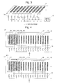
- a two-dimensional photonic crystal 23 is provided on an active layer 21 made of Indium Gallium Arsenide (InGaAs)/Gallium Arsenide (GaAs) and having multiple-quantum wells (MQW) via a lower spacer 22.
- the two-dimensional photonic crystal 23 includes a plate member made of GaAs and having holes 24 periodically arranged in a square lattice pattern.
- the lower spacer 22 and the two-dimensional photonic crystal layer 23 are created as a single layer, in which the holes 24 are present only in the upper portion thereof in order to function as the two-dimensional photonic crystal layer 23 in the upper portion and function as the lower spacer 22 in the lower portion thereof.
- a confining layer 25 made of GaAs, a lower cladding layer 26 made of n-type aluminum gallium arsenide (AlGaAs), and a lower substrate made of n-type GaAs are provided in the descending order from the side closer to the active layer 21.
- the lower substrate is mechanically grinded to obtain a thickness of about 50 to 100 micrometers, followed by depositing gold, germanium and nickel thereon, which are heated at about 400 °C to be alloyed, making a lower electrode 27.
- an upper spacer 28 made of GaAs, an upper cladding layer 29 made of p-type AlGaAs, and a contact layer 30 made of p-type GaAs are provided in the ascending order from the side closer to the two-dimensional photonic crystal 23.
- Each of these layers can be manufactured by a method similar to that of Patent Document 2.
- upper electrodes 22 are linearly arranged on the contact layer 30.
- the plane shape of upper electrodes 33 is rectangle laid long vertical to the array direction.
- gold can be used, for example..
- An electrode using gold is capable of suppressing a current loss to a minimum level, and can be manufactured easily by, for example, a deposition method.
- a transparent electrode made of Zinc Oxide (ZnO) in which carriers are doped may be used in the upper electrodes 33. Using such a transparent electrode allows extraction of a larger amount of light to the outside.
- ZnO Zinc Oxide
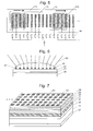
- the lower electrode 27 and each of the upper electrodes 33 are connected in parallel to a DC power supply as shown in Fig. 3, where a switch 34 made of a transistor or the like is provided in each of the upper electrodes 33.
- a control unit 35 is provided to control the on/off of these switches 34.
- a photonic crystal laser device is thus constructed.
- the photonic crystal laser device of the present embodiment is described referring to Fig. 4.
- four electrodes 331 to 334 disposed on one end are formed into one group out of the large number of the arranged upper electrodes 33, and a voltage is applied between the group of these electrodes and the lower electrode to introduce a current. Therefore, carriers are injected in the active layer 21 in the area directly below the four upper electrodes 331 to 334 and the surrounding area, so that light is generated in the area.
- the light is also introduced into the two-dimensional photonic crystal 23, where the light is diffracted and amplified to produce an oscillation of laser.
- the two-dimensional photonic crystal 23 is created in the area 42.
- the laser light is radiated in the direction vertical to the surface of the photonic crystal 23 and emitted from the contact layer 30 to the outside.
- the area around the four upper electrodes 331 to 334 in which a current is introduced becomes a light-emitting area 411 as shown in Fig. 4a.
- the light-emitting area 411 has a shape close to a square since the area into which a current is introduced is set to be a shape close to a square while each of the uppler electrodes 331 to 334 is shaped long rectangle lying vertical to the array direction.
- the current to the leftmost upper electrode 331 in the four electrodes is turned off, and simultaneously a current is introduced to the adjacent upper electrode 335 on the right side (Fig. 4b). This causes the light-emitting area to shift from 411 to 412.
- the switching of each of the upper electrodes is thus controlled by the control unit 35 and the current-introducing upper electrodes are successively switched, so that the light-emitting area can be shifted in the direction of the array of the upper electrodes 33.
- the operation is repeated in such a manner that: the light-emitting area moves from the left end to the right end of the element in almost continuous manner, returns to the left end of the element, and then again moves from the left end to the right end in almost continuous manner.
- This operation is the same as that of a laser light scan in the laser printer shown in Fig. 1.
- the number of upper electrodes into which a current is simultaneously introduced is not limited to four as shown above.
- a current may be exclusively introduced to each one of the upper electrodes for each time.
- the light-emitting area is controlled to return to the left end of the element immediately after reaching the right end of the element in the above example, the light-emitting area may return to the left end from the right end in the opposite direction after reaching the right end, depending on purposes.
- the shape of the upper electrodes 33 is not limited to a rectangle laid long vertical to the array direction as stated above, and may be, for example, a square or other shape. Moreover, the electrodes may be two-dimensionally arranged to scan a single beam in various directions or scan a plurality of beams simultaneously.
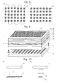
- Fig. 6 shows an example in which a means for changing (or deflecting) the direction of a laser light is provided for each of the upper electrodes 33.
- one lens 61 is provided above the photonic crystal laser element so as to cover the entire upper electrodes 33. Owing to this, the range of a laser light radiation is extended in the array direction of the upper electrodes 33, which allows an expansion of an irradiation area (or scanning area) of a laser light while minimizing the size of the photonic crystal laser element.
- Embodiments of the photonic crystal laser element and the photonic crystal laser device according to the present invention are not limited to the above examples.
- the upper electrodes 33 may be arranged two-dimensionally as shown in Fig. 7.
- the current-injecting upper electrodes 33 are switched in the order shown by the arrow of Fig. 8a, the light-emitting area can be scanned two-dimensionally.
- a plurality of laser lights can be scanned simultaneously.
- the upper electrodes 33 may be created as a single electrode and the plurality of lower electrodes 32 may be created on the substrate 31.
- This photonic crystal laser element is operated in the same manner with the above embodiment.
- Fig. 10 shows an example of using the photonic crystal laser element according to the present invention in a light source unit of a laser printer.
- a photonic crystal laser element 71 having the same length as an effective print width of a photoreceptor drum 73 is made and placed in a position facing the photoreceptor drum 73.
- the upper electrodes can be made sufficiently small (the arrangement pitch was about 20 ⁇ m in the above example) while allowing an oscillation of laser, such a construction is feasible according to the present invention.
- a photonic crystal laser element 72 shorter than the effective print width of the photoreceptor drum 73 and having the same number of upper electrodes as the above example is made and placed in a position facing the photoreceptor drum 73.
- the size (or length) of the photonic crystal laser element 72 is 1/10 of the effective print width of the photoreceptor drum 73 (i.e. 2.54 cm in the above example)
- the pitch to arrange the upper electrodes is about 2 ⁇ m, which is possible enough by using a short wavelength laser.
- the lens 61 is arranged on the photonic crystal laser element as shown in Fig. 6, or a lens 74 is provided separately from the photonic crystal laser element and placed between the photonic crystal laser element light source and the photoreceptor drum 73, in order to expand a laser light from the photonic crystal laser element in a wide range.
- a light emission control of a laser light is made by controlling on/off of the voltage applied to each of the upper electrodes in the photonic crystal laser element light source, so that a laser light scan is performed on the photoreceptor drum 73 in the same manner as the conventional laser printers.
- An electronic scanning process can be thus achieved without using a polygon mirror, which allows a significantly high-speed printing process.
Landscapes
- Physics & Mathematics (AREA)
- Optics & Photonics (AREA)
- Condensed Matter Physics & Semiconductors (AREA)
- General Physics & Mathematics (AREA)
- Electromagnetism (AREA)
- Health & Medical Sciences (AREA)
- General Health & Medical Sciences (AREA)
- Toxicology (AREA)
- Semiconductor Lasers (AREA)
- Optical Modulation, Optical Deflection, Nonlinear Optics, Optical Demodulation, Optical Logic Elements (AREA)
Applications Claiming Priority (1)
| Application Number | Priority Date | Filing Date | Title |
|---|---|---|---|
| PCT/JP2005/008173 WO2006117863A1 (ja) | 2005-04-28 | 2005-04-28 | フォトニック結晶レーザ |
Publications (2)
| Publication Number | Publication Date |
|---|---|
| EP1879272A1 true EP1879272A1 (de) | 2008-01-16 |
| EP1879272A4 EP1879272A4 (de) | 2008-06-18 |
Family
ID=37307670
Family Applications (1)
| Application Number | Title | Priority Date | Filing Date |
|---|---|---|---|
| EP05737342A Withdrawn EP1879272A4 (de) | 2005-04-28 | 2005-04-28 | Laser mit photonischem kristall |
Country Status (3)
| Country | Link |
|---|---|
| US (1) | US7860141B2 (de) |
| EP (1) | EP1879272A4 (de) |
| WO (1) | WO2006117863A1 (de) |
Cited By (4)
| Publication number | Priority date | Publication date | Assignee | Title |
|---|---|---|---|---|
| DE102008054217A1 (de) * | 2008-10-31 | 2010-05-06 | Osram Opto Semiconductors Gmbh | Optoelektronischer Halbleiterchip und Verfahren zur Herstellung eines optoelektronischen Halbleiterchips |
| US8155163B2 (en) | 2007-03-23 | 2012-04-10 | Sumitomo Electric Industries, Ltd. | Photonic crystal laser and method of manufacturing photonic crystal laser |
| US20130243026A1 (en) * | 2012-02-28 | 2013-09-19 | Rohm Co., Ltd. | Two-dimensional photonic crystal surface emitting laser |
| EP4131675A4 (de) * | 2020-03-31 | 2023-09-20 | Kyoto University | Zweidimensionaler laser mit photonischem kristall |
Families Citing this family (8)
| Publication number | Priority date | Publication date | Assignee | Title |
|---|---|---|---|---|
| JP5070161B2 (ja) * | 2007-08-31 | 2012-11-07 | 独立行政法人科学技術振興機構 | フォトニック結晶レーザ |
| WO2012082523A2 (en) | 2010-12-16 | 2012-06-21 | California Institute Of Technology | Chemically-etched nanostructures and related devices |
| JP5850366B2 (ja) | 2011-12-06 | 2016-02-03 | 国立大学法人京都大学 | 半導体レーザ素子及びレーザビーム偏向装置 |
| JP2014027264A (ja) * | 2012-06-22 | 2014-02-06 | Canon Inc | 面発光レーザ |
| DE102014119435B4 (de) * | 2014-07-23 | 2017-03-23 | Beijing Lenovo Software Ltd. | Elektronikgerät und Datenverarbeitungsverfahren |
| JP6329893B2 (ja) | 2014-12-24 | 2018-05-23 | 浜松ホトニクス株式会社 | 半導体レーザ装置 |
| US11728621B2 (en) * | 2019-06-05 | 2023-08-15 | Stmicroelectronics (Research & Development) Limited | Voltage controlled steered VCSEL driver |
| US11579290B2 (en) | 2019-06-05 | 2023-02-14 | Stmicroelectronics (Research & Development) Limited | LIDAR system utilizing multiple networked LIDAR integrated circuits |
Family Cites Families (21)
| Publication number | Priority date | Publication date | Assignee | Title |
|---|---|---|---|---|
| JPH01239979A (ja) | 1988-03-22 | 1989-09-25 | Seiko Epson Corp | ビーム走査型半導体レーザ |
| JPH06196806A (ja) | 1992-12-25 | 1994-07-15 | Sanyo Electric Co Ltd | 面発光レーザ素子 |
| JPH07321401A (ja) * | 1994-05-27 | 1995-12-08 | Fuji Xerox Co Ltd | 半導体レーザアレイとその駆動方法 |
| JP3713725B2 (ja) | 1994-09-28 | 2005-11-09 | 富士ゼロックス株式会社 | 半導体レーザ装置、その製造方法およびその駆動方法 |
| TW289175B (de) * | 1995-04-07 | 1996-10-21 | Mitsubishi Electric Corp | |
| US6052399A (en) | 1997-08-29 | 2000-04-18 | Xerox Corporation | Independently addressable laser array with native oxide for optical confinement and electrical isolation |
| JP2000020995A (ja) | 1998-07-01 | 2000-01-21 | Konica Corp | レーザーアレイ光学系 |
| JP3983933B2 (ja) * | 1999-05-21 | 2007-09-26 | 進 野田 | 半導体レーザ、および半導体レーザの製造方法 |
| DK1371120T3 (da) | 2001-03-09 | 2013-07-22 | Alight Photonics Aps | Bølgetypekontrol ved anvendelse af transversal båndgabsstruktur i vcsels |
| US20030091084A1 (en) | 2001-11-13 | 2003-05-15 | Decai Sun | Integration of VCSEL array and microlens for optical scanning |
| AU2003207090A1 (en) * | 2002-02-08 | 2003-09-02 | Matsushita Electric Industrial Co., Ltd. | Semiconductor light-emitting device and its manufacturing method |
| JP4185697B2 (ja) | 2002-03-14 | 2008-11-26 | 独立行政法人科学技術振興機構 | 2次元フォトニック結晶面発光レーザアレイ及び2次元フォトニック結晶面発光レーザ |
| JP2003273454A (ja) * | 2002-03-14 | 2003-09-26 | Japan Science & Technology Corp | 2次元フォトニック結晶面発光レーザ |
| JP2003273456A (ja) | 2002-03-14 | 2003-09-26 | Japan Science & Technology Corp | 2次元フォトニック結晶面発光レーザ |
| US6665322B2 (en) * | 2002-03-19 | 2003-12-16 | San Jose Systems Inc. | Method and apparatus for controlling the length of an optical cavity |
| JP2004087980A (ja) | 2002-08-28 | 2004-03-18 | Sony Corp | 端面発光型半導体レーザ、電子機器、端面発光型半導体レーザの制御方法及び端面発光型半導体レーザの製造方法 |
| JP2004228122A (ja) | 2003-01-20 | 2004-08-12 | Sony Corp | 発光素子及びその作製方法 |
| US6826223B1 (en) * | 2003-05-28 | 2004-11-30 | The United States Of America As Represented By The Secretary Of The Navy | Surface-emitting photonic crystal distributed feedback laser systems and methods |
| JP4092570B2 (ja) * | 2003-07-23 | 2008-05-28 | セイコーエプソン株式会社 | 光素子およびその製造方法、光モジュール、ならびに光モジュールの駆動方法 |
| DE602004024451D1 (de) * | 2003-12-22 | 2010-01-14 | Panasonic Corp | Halbleiterlaser-bauelement und laserprojektor |
| JP4711324B2 (ja) | 2004-03-25 | 2011-06-29 | 国立大学法人京都大学 | フォトニック結晶レーザ |
-
2005
- 2005-04-28 US US11/919,344 patent/US7860141B2/en not_active Expired - Lifetime
- 2005-04-28 EP EP05737342A patent/EP1879272A4/de not_active Withdrawn
- 2005-04-28 WO PCT/JP2005/008173 patent/WO2006117863A1/ja not_active Ceased
Cited By (6)
| Publication number | Priority date | Publication date | Assignee | Title |
|---|---|---|---|---|
| US8155163B2 (en) | 2007-03-23 | 2012-04-10 | Sumitomo Electric Industries, Ltd. | Photonic crystal laser and method of manufacturing photonic crystal laser |
| DE102008054217A1 (de) * | 2008-10-31 | 2010-05-06 | Osram Opto Semiconductors Gmbh | Optoelektronischer Halbleiterchip und Verfahren zur Herstellung eines optoelektronischen Halbleiterchips |
| US8536603B2 (en) | 2008-10-31 | 2013-09-17 | Osram Opto Semiconductors Gmbh | Optoelectronic semiconductor chip and method of producing an optoelectronic semiconductor chip |
| US20130243026A1 (en) * | 2012-02-28 | 2013-09-19 | Rohm Co., Ltd. | Two-dimensional photonic crystal surface emitting laser |
| US9088133B2 (en) * | 2012-02-28 | 2015-07-21 | Kyoto University | Two-dimensional photonic crystal surface emitting laser |
| EP4131675A4 (de) * | 2020-03-31 | 2023-09-20 | Kyoto University | Zweidimensionaler laser mit photonischem kristall |
Also Published As
| Publication number | Publication date |
|---|---|
| EP1879272A4 (de) | 2008-06-18 |
| US20090034566A1 (en) | 2009-02-05 |
| WO2006117863A1 (ja) | 2006-11-09 |
| US7860141B2 (en) | 2010-12-28 |
Similar Documents
| Publication | Publication Date | Title |
|---|---|---|
| US7860141B2 (en) | Photonic crystal laser | |
| US5727014A (en) | Vertical-cavity surface-emitting laser generating light with a defined direction of polarization | |
| KR101117018B1 (ko) | 면발광 레이저, 면발광 레이저 어레이, 광 주사 장치, 화상 형성 기기, 광 전송 모듈, 및 광 전송 시스템 | |
| US7098993B2 (en) | Exposure device for exposing a photosensitive material in accordance with image data | |
| TW200416639A (en) | Organic vertical cavity laser and imaging system | |
| EP0755147A2 (de) | Bilderzeugungsgerät | |
| US8416826B2 (en) | Photonic crystal surface emitting laser | |
| US20070097680A1 (en) | Light-emitting photonic device | |
| KR950024381A (ko) | 원형 그레이팅 표면 방출형 레이저 다이오드 및 그어레이 | |
| US20080137704A1 (en) | Tuneable unipolar lasers | |
| JPH06224518A (ja) | サーフェススキミングレーザを作るためのモノリシック半導体デバイス | |
| JP4711324B2 (ja) | フォトニック結晶レーザ | |
| JP2784025B2 (ja) | 光走査装置 | |
| JP3713725B2 (ja) | 半導体レーザ装置、その製造方法およびその駆動方法 | |
| US10490692B2 (en) | Semiconductor light-emitting device and display apparatus | |
| KR100866059B1 (ko) | 대구경 표면 발광형 반도체 레이저 소자를 이용한 광정보처리 장치 | |
| KR102936237B1 (ko) | 레이저 마킹 시스템 및 방법 | |
| KR100754064B1 (ko) | 광변조기를 이용한 스캐닝 장치 | |
| EP1139527A2 (de) | Hochleistungsvielfachhalbleiterlaservorrichtung | |
| KR20080017331A (ko) | 포토닉 결정 레이저 | |
| TWI330139B (de) | ||
| JP2014017448A (ja) | 面発光レーザ、面発光レーザアレイ、光走査装置及び画像形成装置 | |
| Alibert et al. | Subnanosecond tunable laser using a single electroabsorption tuning super structure grating | |
| KR20080023085A (ko) | 발광소자 구동방법 및 발광장치 | |
| CN116191199A (zh) | 一种垂直腔面发射激光器及其制备方法 |
Legal Events
| Date | Code | Title | Description |
|---|---|---|---|
| PUAI | Public reference made under article 153(3) epc to a published international application that has entered the european phase |
Free format text: ORIGINAL CODE: 0009012 |
|
| 17P | Request for examination filed |
Effective date: 20071120 |
|
| AK | Designated contracting states |
Kind code of ref document: A1 Designated state(s): DE |
|
| RAP1 | Party data changed (applicant data changed or rights of an application transferred) |
Owner name: ROHM CO., LTD. |
|
| A4 | Supplementary search report drawn up and despatched |
Effective date: 20080520 |
|
| DAX | Request for extension of the european patent (deleted) | ||
| RBV | Designated contracting states (corrected) |
Designated state(s): DE |
|
| 17Q | First examination report despatched |
Effective date: 20080822 |
|
| STAA | Information on the status of an ep patent application or granted ep patent |
Free format text: STATUS: THE APPLICATION IS DEEMED TO BE WITHDRAWN |
|
| 18D | Application deemed to be withdrawn |
Effective date: 20090303 |