EP1880295B1 - Système et procédé pour le decodage de commandes sur la base des signaux de commande et de l'état d'exploitation - Google Patents
Système et procédé pour le decodage de commandes sur la base des signaux de commande et de l'état d'exploitation Download PDFInfo
- Publication number
- EP1880295B1 EP1880295B1 EP06750643.6A EP06750643A EP1880295B1 EP 1880295 B1 EP1880295 B1 EP 1880295B1 EP 06750643 A EP06750643 A EP 06750643A EP 1880295 B1 EP1880295 B1 EP 1880295B1
- Authority
- EP
- European Patent Office
- Prior art keywords
- command
- state
- memory
- memory system
- signals
- Prior art date
- Legal status (The legal status is an assumption and is not a legal conclusion. Google has not performed a legal analysis and makes no representation as to the accuracy of the status listed.)
- Expired - Lifetime
Links
Images




Classifications
-
- G—PHYSICS
- G11—INFORMATION STORAGE
- G11C—STATIC STORES
- G11C7/00—Arrangements for writing information into, or reading information out from, a digital store
- G11C7/10—Input/output [I/O] data interface arrangements, e.g. I/O data control circuits, I/O data buffers
- G11C7/1072—Input/output [I/O] data interface arrangements, e.g. I/O data control circuits, I/O data buffers for memories with random access ports synchronised on clock signal pulse trains, e.g. synchronous memories, self timed memories
-
- G—PHYSICS
- G11—INFORMATION STORAGE
- G11C—STATIC STORES
- G11C11/00—Digital stores characterised by the use of particular electric or magnetic storage elements; Storage elements therefor
- G11C11/21—Digital stores characterised by the use of particular electric or magnetic storage elements; Storage elements therefor using electric elements
- G11C11/34—Digital stores characterised by the use of particular electric or magnetic storage elements; Storage elements therefor using electric elements using semiconductor devices
- G11C11/40—Digital stores characterised by the use of particular electric or magnetic storage elements; Storage elements therefor using electric elements using semiconductor devices using transistors
- G11C11/401—Digital stores characterised by the use of particular electric or magnetic storage elements; Storage elements therefor using electric elements using semiconductor devices using transistors forming cells needing refreshing or charge regeneration, i.e. dynamic cells
- G11C11/4063—Auxiliary circuits, e.g. for addressing, decoding, driving, writing, sensing or timing
- G11C11/407—Auxiliary circuits, e.g. for addressing, decoding, driving, writing, sensing or timing for memory cells of the field-effect type
- G11C11/409—Read-write [R-W] circuits
- G11C11/4096—Input/output [I/O] data management or control circuits, e.g. reading or writing circuits, I/O drivers or bit-line switches
-
- G—PHYSICS
- G06—COMPUTING OR CALCULATING; COUNTING
- G06F—ELECTRIC DIGITAL DATA PROCESSING
- G06F9/00—Arrangements for program control, e.g. control units
- G06F9/06—Arrangements for program control, e.g. control units using stored programs, i.e. using an internal store of processing equipment to receive or retain programs
- G06F9/30—Arrangements for executing machine instructions, e.g. instruction decode
-
- G—PHYSICS
- G11—INFORMATION STORAGE
- G11C—STATIC STORES
- G11C11/00—Digital stores characterised by the use of particular electric or magnetic storage elements; Storage elements therefor
- G11C11/21—Digital stores characterised by the use of particular electric or magnetic storage elements; Storage elements therefor using electric elements
- G11C11/34—Digital stores characterised by the use of particular electric or magnetic storage elements; Storage elements therefor using electric elements using semiconductor devices
- G11C11/40—Digital stores characterised by the use of particular electric or magnetic storage elements; Storage elements therefor using electric elements using semiconductor devices using transistors
- G11C11/401—Digital stores characterised by the use of particular electric or magnetic storage elements; Storage elements therefor using electric elements using semiconductor devices using transistors forming cells needing refreshing or charge regeneration, i.e. dynamic cells
- G11C11/406—Management or control of the refreshing or charge-regeneration cycles
- G11C11/40611—External triggering or timing of internal or partially internal refresh operations, e.g. auto-refresh or CAS-before-RAS triggered refresh
-
- G—PHYSICS
- G11—INFORMATION STORAGE
- G11C—STATIC STORES
- G11C11/00—Digital stores characterised by the use of particular electric or magnetic storage elements; Storage elements therefor
- G11C11/21—Digital stores characterised by the use of particular electric or magnetic storage elements; Storage elements therefor using electric elements
- G11C11/34—Digital stores characterised by the use of particular electric or magnetic storage elements; Storage elements therefor using electric elements using semiconductor devices
- G11C11/40—Digital stores characterised by the use of particular electric or magnetic storage elements; Storage elements therefor using electric elements using semiconductor devices using transistors
- G11C11/401—Digital stores characterised by the use of particular electric or magnetic storage elements; Storage elements therefor using electric elements using semiconductor devices using transistors forming cells needing refreshing or charge regeneration, i.e. dynamic cells
- G11C11/4063—Auxiliary circuits, e.g. for addressing, decoding, driving, writing, sensing or timing
- G11C11/407—Auxiliary circuits, e.g. for addressing, decoding, driving, writing, sensing or timing for memory cells of the field-effect type
- G11C11/4076—Timing circuits
-
- G—PHYSICS
- G11—INFORMATION STORAGE
- G11C—STATIC STORES
- G11C11/00—Digital stores characterised by the use of particular electric or magnetic storage elements; Storage elements therefor
- G11C11/21—Digital stores characterised by the use of particular electric or magnetic storage elements; Storage elements therefor using electric elements
- G11C11/34—Digital stores characterised by the use of particular electric or magnetic storage elements; Storage elements therefor using electric elements using semiconductor devices
- G11C11/40—Digital stores characterised by the use of particular electric or magnetic storage elements; Storage elements therefor using electric elements using semiconductor devices using transistors
- G11C11/401—Digital stores characterised by the use of particular electric or magnetic storage elements; Storage elements therefor using electric elements using semiconductor devices using transistors forming cells needing refreshing or charge regeneration, i.e. dynamic cells
- G11C11/4063—Auxiliary circuits, e.g. for addressing, decoding, driving, writing, sensing or timing
- G11C11/407—Auxiliary circuits, e.g. for addressing, decoding, driving, writing, sensing or timing for memory cells of the field-effect type
- G11C11/408—Address circuits
- G11C11/4087—Address decoders, e.g. bit - or word line decoders; Multiple line decoders
-
- G—PHYSICS
- G11—INFORMATION STORAGE
- G11C—STATIC STORES
- G11C11/00—Digital stores characterised by the use of particular electric or magnetic storage elements; Storage elements therefor
- G11C11/21—Digital stores characterised by the use of particular electric or magnetic storage elements; Storage elements therefor using electric elements
- G11C11/34—Digital stores characterised by the use of particular electric or magnetic storage elements; Storage elements therefor using electric elements using semiconductor devices
- G11C11/40—Digital stores characterised by the use of particular electric or magnetic storage elements; Storage elements therefor using electric elements using semiconductor devices using transistors
- G11C11/401—Digital stores characterised by the use of particular electric or magnetic storage elements; Storage elements therefor using electric elements using semiconductor devices using transistors forming cells needing refreshing or charge regeneration, i.e. dynamic cells
- G11C11/4063—Auxiliary circuits, e.g. for addressing, decoding, driving, writing, sensing or timing
- G11C11/407—Auxiliary circuits, e.g. for addressing, decoding, driving, writing, sensing or timing for memory cells of the field-effect type
- G11C11/409—Read-write [R-W] circuits
- G11C11/4091—Sense or sense/refresh amplifiers, or associated sense circuitry, e.g. for coupled bit-line precharging, equalising or isolating
Definitions
- the invention relates generally to command decoding for a memory system, and more particularly, to decoding command signals to perform operations in the memory system based on the command signals and a operating state of the memory system.
- Computer systems use memory devices, such as synchronous dynamic random access memory (“SDRAM”) devices, to store instructions and data that are access by a processor. These memory devices are normally used as system memory in a computer system.
- the processor communicates with the system memory through a processor bus and a memory controller.
- the processor issues a memory request, which includes a memory command, such as a read command, and an address designating the location from which data or instructions are to be read.
- the memory controller uses the command and address to generate appropriate command signals as well as row and column addresses, which are applied to the system memory.
- data is transferred between the system memory and the processor.
- FIG 1 is a functional block diagram of a conventional memory device 100.
- the memory device 100 in Figure 1 is an example of a double-data rate (DDR) SDRAM.
- the memory device 100 is referred to as a double-data-rate device.because the data words DQ being transferred to and from the device are transferred at double the rate of a conventional SDRAM, which transfers data at a rate corresponding to the frequency of the applied clock signal.
- the memory device 100 includes a control logic and command decoder 134 that receives a plurality of command and clock signals over a control bus CONT, typically from an external circuit such as a memory controller (not shown).
- the command signals include a chip select signal CS#, a write enable signal WE#, a column address strobe signal CAS#, and a row address strobe signal RAS#, while the clock signals include a clock enable signal CKE# and complementary clock signals CLK, CLK#, with the "#" designating a signal as being active LOW.
- the command signals RAS#, CAS#, and WE# are driven to values corresponding to a particular command, such as a read, write, or auto-refresh command.
- the command decoder 134 In response to the clock signals CLK, CLK#, the command decoder 134 latches and decodes an applied command, and generates a sequence of internal clock and control signals that control the components 102-132 to execute the function of the applied command.
- the clock enable signal CKE enables clocking of the command decoder 134 by the clock signals CLK, CLK#.
- the command decoder 134 further includes mode registers 136. Data written to the mode registers 136 are used to set various modes of operation, for example, burst data length, burst type, power-down mode, CAS latency, and the like.
- the command decoder 134 will generate the appropriate internal clock and control signals based on the modes set by the data stored in the mode registers 136.
- the memory device 100 further includes an address register 102 that receives row, column, and bank addresses over an address bus ADDR, with a memory controller (not shown) typically supplying the addresses.
- the address register 102 receives a row address and a bank address that are applied to a row address multiplexer 104 and bank control logic circuit 106, respectively.
- the row address multiplexer 104 applies either the row address received from the address register 102 or a refresh row address from a refresh counter 108 to a plurality of row address latch and decoders 110A-D.
- the bank control logic 106 activates the row address latch and decoder 110A-D corresponding to either the bank address received from the address register 102 or a refresh bank address from the refresh counter 108, and the activated row address latch and decoder latches and decodes the received row address.
- the activated row address latch and decoder 110A-D applies various signals to a corresponding memory bank 112A-D to thereby activate a row of memory cells corresponding to the decoded row address.
- Each memory bank 112A-D includes a memory-cell array having a plurality of memory cells arranged in rows and columns, and the data stored in the memory cells in the activated row is stored in sense amplifiers in the corresponding memory bank.
- the row address multiplexer 104 applies the refresh row address from the refresh counter 108 to the decoders 110A-D and the bank control logic circuit 106 uses the refresh bank address from the refresh counter when the memory device 100 operates in an auto-refresh or self-refresh mode of operation in response to an auto- or self-refresh command being applied to the memory device 100, as will be appreciated by those skilled in the art.
- a column address is applied on the ADDR bus after the row and bank addresses, and the address register 102 applies the column address to a column address counter and latch 114 which, in turn, latches the column address and applies the latched column address to a plurality of column decoders 116A-D.
- the bank control logic 106 activates the column decoder 116A-D corresponding to the received bank address, and the activated column decoder decodes the applied column address.
- the column address counter and latch 114 either directly applies the latched column address to the decoders 116A-D, or applies a sequence of column addresses to the decoders starting at the column address provided by the address register 102.
- the activated column decoder 116A-D applies decode and control signals to an I/O gating and data masking circuit 118 which, in turn, accesses memory cells corresponding to the decoded column address in the activated row of memory cells in the memory bank 112A-D being accessed.
- data being read from the addressed memory cells is coupled through the I/O gating and data masking circuit 118 to a read latch 120.
- the I/O gating and data masking circuit 118 supplies N bits of data to the read latch 120, which then applies two N/4 bit words to a multiplexer 122.
- the circuit 118 provides 32 bits to the read latch 120 which, in turn, provides four 8 bits words to the multiplexer 122.
- a data driver 124 sequentially receives the N/4 bit words from the multiplexer 122 and also receives a data strobe signal DQS from a strobe signal generator 126 and a delayed clock signal CLKDEL from the delay-locked loop 123.
- the DQS signal is used by an external circuit such as a memory controller (not shown) in latching data from the memory device 100 during read operations.
- the data driver 124 sequentially outputs the received N/4 bits words as a corresponding data word DQ, each data word being output in synchronism with a rising or falling edge of a CLK signal that is applied to clock the memory device 100.
- the data driver 124 also outputs the data strobe signal DQS having rising and falling edges in synchronism with rising and falling edges of the CLK signal, respectively.
- Each data word DQ and the data strobe signal DQS collectively define a data bus DATA.
- the DATA bus also includes masking signals DM0-M for masking write data of data write operations, as will be described in more detail below.
- an external circuit such as a memory controller (not shown) applies N/4 bit data words DQ, the strobe signal DQS, and corresponding data masking signals DM on the data bus DATA.
- a data receiver 128 receives each DQ word and the associated DM signals, and applies these signals to input registers 130 that are clocked by the DQS signal. In response to a rising edge of the DQS signal, the input registers 130 latch a first N/4 bit DQ word and the associated DM signals, and in response to a falling edge of the DQS signal the input registers latch the second N/4 bit DQ word and associated DM signals.
- the input register 130 provides the two latched N/4 bit DQ words as an N-bit word to a write FIFO and driver 132, which clocks the applied DQ word and DM signals into the write FIFO and driver in response to the DQS signal.
- the DQ word is clocked out of the write FIFO and driver 132 in response to the CLK signal, and is applied to the I/O gating and masking circuit 118.
- the I/O gating and masking circuit 118 transfers the DQ word to the addressed memory cells in the accessed bank 112A-D subject to the DM signals, which may be used to selectively mask bits or groups of bits in the DQ words (i.e., in the write data) being written to the addressed memory cells.
- commands are issued to the memory device 100 in the form of command signals, which are decoded by the command decoder 134 to generate internal clock and control signals to perform the requested operation.
- Figure 2 is a command decoding truth table for the memory device 100.
- the three command signals RAS#, CAS#, and WE# provide eight different commands for the memory device 100. These commands include LOAD MODE, REFRESH, PRECHARGE, BANK ACTIVATE, WRITE, READ, NOP (no operation), and a RESERVED command, which can be used in the future for an additional command.
- the LOAD MODE command is used to load data into the mode registers 136, which, as previously discussed, is used to set various modes of operation, for example, burst data length, burst type, power-down mode, CAS latency, and the like.
- the REFRESH command is used to invoke a refresh sequence in the memory banks 112A-D.
- the PRECHARGE command is used to deactivate or "close” activated, or "open,” memory banks 112A-D.
- the BANK ACTIVATE command is used to open at least one of the memory banks 112A-D, as selected by a bank address, in preparation for an memory access operation.
- the WRITE command and the READ command are used to invoke a data write operation and a data read operation, respectively, as previously described.
- the NOP operation is used to prevent unwanted commands from being registered during idle or wait states of the memory device 100.
- RAS#, CAS#, and WE# signals provide an effective way to issue commands to the memory device 100.
- One such limitation is the maximum number of different possible commands that are provided with the conventional command decoding of the memory device 100.
- the three command signals provide a maximum decoding of eight different commands. Although eight different commands are sufficient for current technology, it is easy to imagine that in the future there may be the need for more than the eight commands previously described. If additional commands are desired, additional command signals will need to be used. For example, if two additional commands for a total of ten commands are desired, one command could be decoded using the RESERVED command. However, the other additional command would require adding one more signal to the existing three commands signals. With four command signals, there are now potentially sixteen different commands that can be decoded.
- US6233195 and US2003007405 each discloses a method for executing a memory command in a memory system which may perform additional internal operations to carry out the requested command based on the operating status of the memory system.
- US6629224B1 describes a memory device in which the number of operating modes is sequentially narrowed down based on signals supplied as commands.
- Embodiments of the present invention are directed to a memory system as defined in appended claim 1, computer processing system as defined in appended claim 8 and method for decoding command signals as defined in appended claim 20. Preferred 35 embodiments are defined in the remaining appended claims.
- a command decoder is configured to generate internal control signals to perform an operation selected from a first set of operations according to the latched logic levels of the command signals when the memory system is in a first operating state.
- the command decoder is further configured to generate internal control signals to perform an operation selected from a second set of operations according to the latched logic levels of the command signals when the memory system is in a second operating state.
- a method of decoding command signals includes receiving command signals, and selecting one operation from a first set of operations in accordance with the command signals while the memory system is in a first operating state, and selecting one operation from a second set of operations in accordance with the command signals while the memory system is in a second operating state.
- Embodiments of the present invention provide systems and methods for command decoding in a memory that decodes commands based on command signals in combination with an operating state of the memory. Certain details are set forth below to provide a sufficient understanding of the invention. However, it will be clear to one skilled in the art that the invention may be practiced without these particular details. In other instances, well-known circuits, control signals, timing protocols, and software operations have not been shown in detail in order to avoid unnecessarily obscuring the invention.
- Figure 3 illustrates a memory device 300 having control logic and command decoder 334 according to an embodiment of the present invention.
- Many of the circuits included in the memory device 300 have been previously described with respect to the memory device 100 of Figure 1 , and consequently, in the interest of brevity, will not be described again. Operation of these circuits in the memory device 300 are the same as in previously described with respect to the memory device 100 of Figure 1 , and are referenced in Figure 3 using the same reference number.
- the command decoder 334 is different than the command decoder 134 of the memory device 100.
- the command decoder 334 decodes command signals applied to the memory device 300 and generates internal clock and control signals to execute the requested command based on the command signals in combination with a operating state of the memory device 300.
- the command decoder 334 generates the internal signals to perform a requested operation based on the set of command signals applied to the memory device 300 and its current operating state.
- the number of command signals needed for decoding the commands can be reduced while maintaining the same number of different commands available.
- the number of different commands can be increased without increasing the number of command signals.
- the memory device 300 has the same number of commands as previously described for the memory device 100, and shown in the table of Figure 2 .
- the eight different commands are LOAD MODE REGISTERS, REFRESH, PRECHARGE, BANK ACTIVATE, WRITE, READ, RESERVED, and NOP.
- These eight commands for the memory device 100 can be selected based on the combination of the logic states of the three command signals RAS#, CAS#, and WE#.
- the memory device 300 can select one of the same eight commands using only two command signals, RAS# and WE#, in combination with monitoring a bank active state.
- the command decoder 334 is coupled to the bank control logic 306 to receive a bank active state signal BACTIVE having a logic state indicative of whether any of the memory banks 112A-D are "open” ( i.e., active) or if all of the banks are "closed” ( i.e., precharged).
- Figure 4 illustrates a truth table for command decoding in the memory device 300 of Figure 3 according to an embodiment of the present invention.
- Column 402 lists the commands for different combinations of the RAS# and WE# signals when any of the memory banks 312A-D are open.
- Column 404 lists the commands for different combinations of the RAS# and WE# signals for when all of the memory banks 312A-D are closed.
- the command decoder 334 will generate internal clock and control signals to execute a WRITE operation to at least one memory location in the memory banks 312A-D identified by the address and bank signals, as previously described.
- the command decoder 334 will generate internal clock and control signals to execute a LOAD MODE command that loads mode information into the mode register 136, as previously described.
- the memory device 300 has the same eight commands as the memory device 100, but only requires the two RAS# and WE# signals instead of the three RAS#, CAS#, and WE# signals.
- Figure 5 is a state diagram illustrating the command decoding of the memory device 300 as previously described with respect to the command decoding truth table of Figure 4 .
- Figure 5 illustrates various memory device operations, represented by circles, and various memory device states, represented by shaded circles.
- the memory device 300 changes states and performs operations in response to command signals RAS# and WE#, with command sequences (defined by a combination of command signals) and changes of state represented by arrows pointing from a memory device state to a memory device operation.
- Bold arrows in Figure 5 represent an automatic sequence that returns the memory device 300 to a memory device state upon completion of the memory device operation.
- Figure 5 illustrates command decoding on a per bank basis for memory banks 0 to N, which correspond to the memory banks 112A-D of the memory device 300.
- Memory bank selection is made by way of bank addresses applied to the memory device at the time the command signals are latched.
- a power-on sequence is executed to place the memory device 300 in a POWER ON state 502.
- the memory device 300 exits the POWER ON state 502 and is reset to an ALL BANK PRECHARGED state 504.
- ALL BANK PRECHARGED state 504 and all of the memory banks 112A-D are closed, application of the RAS# and WE# signals are be decoded by the command decoder 334 into one of three commands (not including the RESERVED command).
- the three commands shown in Figure 5 are a REFRESH command that causes the memory device 300 to execute an AUTO REFRESH operation 506, a LOAD MODE command that causes the memory device 300 to execute an LOAD MRS operation 508, or a BANK ACTIVATE command that causes the memory device 300 to execute an ACTIVATE BANK command 509 for a particular memory bank 0 through N.
- the REFRESH command is decoded from a LOW RAS# signal and a LOW WE# signal applied to the command decoder 334 while the memory device 300 is in the ALL BANK PRECHARGED state 504.
- the memory device 300 changes from the ALL BANK PRECHARGED state 504 to execute the AUTO REFRESH sequence 506.
- the AUTO REFRESH sequence 506 is completed, the memory device 300 returns to the ALL BANK PRECHARGED state 504, as shown by the bold arrow pointing from the AUTO REFRESH state 506 back to the ALL BANK PRECHARGED state 504, to await further commands.
- the LOAD MODE command is decoded from a HIGH RAS# signal and a LOW WE# signal while the memory device 300 is in the ALL BANK PRECHARGED state 504.
- the LOAD MODE command is shown in Figure 5 as "WR" representing the combination of a HIGH RAS# signal and LOW WE# signal, which would be decoded to a WRITE command if the memory device was in the BANK ACTIVE state 510.
- the state of the memory device 300 changes from the ALL BANK PRECHARGED state 504 to execute the LOAD MRS operation 508, whereupon completion, the memory device 300 returns to the ALL BANK PRECHARGED state 504.
- the third command that can be decoded when the memory device 300 is in the BANK CLOSED state 504 is the BANK ACTIVATE command, decoded from a LOW RAS# signal and a HIGH WE# signal.
- the BANK ACTIVATE command is shown in Figure 5 as "ACT" representing the combination of a LOW RAS# signal and a HIGH WE# signal.
- a BANK ACTIVATE command is a per bank command that activates at least one of the memory banks 312A-D, typically identified by bank address signals.
- the BANK ACTIVATE command causes the memory device 300 to change from the ALL BANK PRECHARGED state 504 to execute an ACTIVATE BANK operation 509 for the particular memory bank.
- the state of the memory device 300 for the particular memory bank changes to a BANK ACTIVE state 510.
- the activated memory bank 312A-D remains activated until a PRECHARGE command is decoded by the memory device 300, whereupon the state of the memory device 300 changes to from the BANK ACTIVE state 510 to execute a PRECHARGE BANK operation 511.
- the memory device 300 Upon completing the PRECHARGE BANK operation 511, the memory device 300 returns through a BANK PRECHARGE state 505 to the ALL BANK PRECHARGED state 504.
- a BANK ACTIVATE command decoded while the memory device 300 is in the BANK PRECHARGE state 505 will execute the ACTIVATE BANK operation 509 and change the state of the memory device 300 to the BANK ACTIVE state 510.
- Two other commands that can be decoded in addition to the PRECHARGE command from the RAS# and WE# signals while the memory device 300 is in the BANK ACTIVE state 510 are a READ command that causes the memory device 300 to execute a READ operation 512 and a WRITE command that causes the memory device 300 to execute a WRITE operation 514.
- a no operation NOP command can also be decoded by the command decoder 334 from the RAS# and WE# signals while the memory device 300 is in the BANK ACTIVE state 510, but as well known, typically does not cause the memory device to perform an operation.
- the memory device does not change states.
- the READ and WRITE commands are decoded, a respective command is executed and upon completion, the memory device 300 returns to the BANK ACTIVE state 510.
- the same specific combination of the RAS# and WE# signals can be decoded by the command decoder 334 to execute different sets of commands depending on the particular operating state of the memory device 300.
- the combination of a LOW RAS# signal and a LOW WE# signal is labeled in the state diagram 500 as "PRE.”
- the PRE combination of the RAS# and WE# signals results in the memory device 300 changing from the ALL BANK PRECHARGED state 504 to execute the AUTO REFRESH operation 506 to perform an auto-refresh sequence.
- the PRE combination of RAS# and WE# signals is applied when the memory device 300 is in the BANK ACTIVE state 510, it causes the memory device 300 to change from the BANK ACTIVE state 510 to the BANK PRECHARGED state 505 by executing the PRECHARGE BANK operation 511.
- the PRE combination of RAS# and WE# signals two different commands can be decoded.
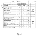
- Figure 6 illustrates a command decoding truth table 600 for the memory device 300 according to an alternative embodiment of the present invention.
- the command decoding truth 600 illustrates the use of an input signal that is not typically used as a command signal to provide additional command decoding choices.
- the address signal A10 is used, in combination with the RAS# and WE# command signals shown in column 602, and further in combination with the memory bank open/closed states shown in column 604, to select a particular refresh or precharge mechanism shown in column 606.
- Conventional memory devices have utilized a signal typically not used for commands, such as the A10 signal, to select different refresh and precharge mechanisms.
- conventional devices do not utilize command decoding as previously described according to an embodiment of the present invention.
- the combination of the command decoding of embodiments of the present invention with the use of a signal not typically used for commands, such as the A10 signal provides additional alternative embodiments of the present invention.
- a refresh command is decoded.
- the logic level of the A10 signal is used to select whether the refresh sequence is executed on a per memory bank basis, or all memory banks 312A-D are refreshed concurrently.
- a LOW A10 signal selects a per memory bank refresh operation and a HIGH A10 signal selects an all memory bank refresh operation.
- the A10 signal is interpreted as part of a valid value when a BANK ACTIVATE command or a LOAD MODE command is issued while the memory device 300 is in the BANK CLOSED state.
- the A10 signal is used to select a refresh sequence when a refresh command is issued during the BANK CLOSED state. Additionally, the A10 signal is used to select various precharge sequences when a precharge command is issued during a BANK OPEN state. As shown in column 608, the A10 signal is used in combination with the RAS# and WE# signals to select single or all bank precharge, auto-precharge following a write command, and auto-precharge following a read command. The A10 signal can be used to select whether an auto-precharge sequence is executed following a write or read command since the A10 signal is not used to select a particular memory location for access.
- Figure 7 illustrates a state diagram 700 for command decoding by the memory device 300 according to another embodiment of the present invention.
- the state diagram 700 of Figure 7 is similar to the state diagram 500 of Figure 5 and uses the same convention as previously described with respect to the memory device state, memory device operation, command sequence and automatic sequences.
- the command decoding can be on a per memory bank basis for memory banks 0 through N.
- the particular memory bank is selected by the bank address signals provided to the memory device 300 at the time the command signals RAS# and WE# are latched.
- additional commands and operating states are defined in the state diagram 700 without increasing the number of command signals. All of the commands and states shown in the state diagram 700 of Figure 7 can be decoded based on the RAS# and WE# signals, in combination with the particular operating state of the memory device 300.
- the POWER down state 702 represents a condition where the memory device 300 is placed into a low-power state during which many of the circuits are deactivated, such as the output drivers 124 ( Figure 3 ), the input receivers 128, and the DLL 123 in order to reduce power consumption.
- the POWER DOWN state 702 can be reached by applying a HIGH RAS# signal and a HIGH WE# signal from the ALL BANK PRECHARGED state 504.
- the state diagram 700 utilizes the RESERVED command to change to the POWER DOWN state 702.
- the RESERVED command is shown in Figure 7 as "RD" representing the combination of a HIGH RAS# signal and a HIGH WE# signal, which is the combination of the command signals for a READ command in a BANK ACTIVE state 510.
- RD the state of the memory device 300 can be changed to a SLEEP POWER DOWN state 704 or a SELF REFRESH state 706 depending on the RAS# and WE# signals applied.
- a HIGH RAS# signal and a HIGH WE# signal are applied to the command decoder 334 when the memory device 300 is in the POWER DOWN state 702, the operating state changes to the SLEEP POWER DOWN state 704.
- the SLEEP POWER DOWN state 704 represents a condition where the memory device 300 is placed into a low-power state to a greater extent than in the POWER DOWN state 702.
- the SLEEP POWER DOWN state 704 may not require a CLK signal to be applied, and consequently, clock buffers of the memory device 300 can be deactivated in addition to the input and output circuits.
- a LOW RAS# signal and a LOW WE# signal are applied to the command decoder 334.
- a LOW RAS# signal and a LOW WE# signal are applied to the command decoder 334.
- the memory device 300 executes a self-refresh sequence to refresh memory cells of the memory banks 312A-D.
- the state of the memory device 300 returns to the POWER DOWN state 702.
- an even greater number of commands can be decoded by applying the specific combination of RAS# and CAS# signals during different operating states of the memory device 300. For example, taking the combination of a LOW RAS# signal and a LOW WE# signal, labeled in the state diagram 700 as "PRE," four different commands can be decoded from the same PRE combination.
- the first command which results from the application of the PRE combination of RAS# and WE# signals during the ALL BANK PRECHARGED state 504, causes the memory device 300 to change from the ALL BANK PRECHARGED state 504 to execute the AUTO REFRESH operation 506.
- the second command which results from application of the PRE combination of the RAS# and WE# signals during the BANK ACTIVE state 510, causes the memory device 300 to execute the PRECHARGE BANK command 511 to change to the BANK PRECHARGED state 505.
- the third command which results from application of the PRE combination of the RAS# and WE# signals during the POWER DOWN state 702, causes the memory device 300 to change to the SELF REFRESH state 706 to execute a self-refresh sequence.
- the fourth command which results from the application of the PRE combination of the RAS# and WE# signals during the SLEEP POWER DOWN state 704 causes the memory device 300 to exit the SLEEP POWER DOWN state 704 to the POWER DOWN state 702.
- FIG. 8 is a block diagram of a processing system 800 including processing circuitry 802 including the memory device 300 having a command decoder 334 that utilizes command decoding according to an embodiment of the present invention.
- the processing circuitry 802 is coupled through address, data, and control buses to the memory device 300 to provide for writing data to and reading data from the memory device.
- the processing circuitry 802 includes circuitry for performing various processing functions, such as executing specific software to perform specific calculations or tasks.
- the processing system 800 includes one or more input devices 804, such as a keyboard or a mouse, coupled to the processing circuitry 802 to allow an operator to interface with the processing system 800.
- the processing system 800 also includes one or more output devices 806 coupled to the processing circuitry 802, such as output devices typically including a printer and a video terminal.
- One or more data storage devices 808 are also typically coupled to the processing circuitry 802 to store data or retrieve data from external storage media (not shown). Examples of typical storage devices 808 include hard and floppy disks, tape cassettes, compact disk read-only (CD-ROMs) and compact disk read-write (CD-RW) memories, and digital video disks (DVDs).
Landscapes
- Engineering & Computer Science (AREA)
- Microelectronics & Electronic Packaging (AREA)
- Computer Hardware Design (AREA)
- Software Systems (AREA)
- Theoretical Computer Science (AREA)
- Databases & Information Systems (AREA)
- Physics & Mathematics (AREA)
- General Engineering & Computer Science (AREA)
- General Physics & Mathematics (AREA)
- Dram (AREA)
- Executing Machine-Instructions (AREA)
- Selective Calling Equipment (AREA)
Claims (30)
- Système de mémoire comprenant une pluralité de commandes et une pluralité d'états de fonctionnement, le système de mémoire comprenant :une pluralité de bancs de mémoire ;un verrou de commande comprenant des noeuds d'entrée de commande au niveau duquel une pluralité de signaux de commande est appliquée, le verrou de commande étant conçu pour verrouiller les signaux de commande ; etun décodeur de commande (334) couplé au verrou de commande, le décodeur de commande étant caractérisé en ce qu'il est conçu pour recevoir un signal d'indication d'un état de fonctionnement courant du système de mémoire et conçu en outre pour décoder une combinaison de signaux de commande, ledit signal ayant un premier état indiquant qu'au moins un banc de la pluralité de bancs du système de mémoire est ouvert afin de configurer le système de mémoire en vue de réaliser une première opération de mémoire demandée et de décoder la combinaison de signaux de commande, et ledit signal ayant un deuxième état indiquant que tous les bancs de la pluralité de bancs du système de mémoire sont fermés afin de configurer le système de mémoire en vue de réaliser une deuxième opération de mémoire demandée différente de la première opération de mémoire demandée.
- Système de mémoire selon la revendication 1, dans lequel le décodeur de commande comprend :un circuit décodeur de commande couplé au verrou de signal de commande, le circuit décodeur de commande étant conçu pour surveiller l'état de fonctionnement du système de mémoire, et étant en outre conçu pour générer des signaux de contrôle interne en vue de réaliser une opération sélectionnée dans un premier ensemble d'opérations de mémoire demandées selon les niveaux logiques verrouillés des signaux de commande quand le système de mémoire est dans un premier état de fonctionnement, et conçu pour générer des signaux de contrôle interne en vue de réaliser une opération sélectionnée dans un deuxième ensemble d'opérations de mémoire demandées selon les niveaux logiques verrouillés des signaux de commande quand le système de mémoire est dans un deuxième état de fonctionnement, le deuxième ensemble d'opérations ayant au moins une opération différente du premier ensemble d'opérations.
- Système de mémoire selon la revendication 1, dans lequel le décodeur de commande comprend :un circuit d'état de fonctionnement, etun circuit décodeur de commande couplé au verrou de commande et au circuit d'état de fonctionnement, le circuit décodeur de commande étant conçu pour générer un premier ensemble de signaux d'horloge et de contrôle afin de réaliser une première opération en réponse à une première combinaison de signaux de commande verrouillés et à une première combinaison de signaux d'état de fonctionnement, et conçu pour générer un deuxième ensemble de signaux d'horloge et de contrôle afin de réaliser une deuxième opération en réponse à la première combinaison de signaux de commande et à une deuxième combinaison de signaux d'état de fonctionnement.
- Système de mémoire selon la revendication 1, comprenant en outre :au moins une matrice de cellules de mémoire (112) comprenant des cellules de mémoire organisées en rangées et en colonnes, la matrice ayant un état actif et un état inactif ;un circuit d'état de matrice couplé à la matrice et conçu pour générer un signal d'état ayant un premier état quand la matrice est dans l'état actif, et ayant un second état quand la matrice est dans l'état inactif ; etdans lequel le décodeur de commande comprend un noeud de commande auquel le signal de commande est appliqué, un noeud d'état de mémoire couplé au circuit d'état de matrice auquel le signal d'état est couplé, et comprend en outre un noeud de signal de contrôle interne auquel sont fournis des signaux de contrôle interne pour l'exécution de commandes de mémoire, le décodeur de commande étant conçu pour générer des signaux de contrôle interne afin d'exécuter une première commande de la pluralité de commandes de mémoire demandées en réponse au signal de commande ayant le premier état et au signal d'état de matrice ayant le premier état, et étant en outre conçu pour générer des signaux de contrôle interne afin d'exécuter une seconde commande de la pluralité de commandes de mémoire demandées en réponse au signal de commande ayant le premier état et au signal d'état de matrice ayant le second état.
- Système de mémoire selon la revendication 2, dans lequel le circuit décodeur de commande du décodeur de commande est en outre conçu pour générer des signaux de contrôle interne afin de réaliser une première opération en réponse à la réception d'une combinaison de niveaux logiques verrouillés des signaux de commande quand le système de mémoire est dans le premier état de fonctionnement, et conçu pour générer des signaux de contrôle interne afin de réaliser une deuxième opération en réponse à la réception d'une combinaison de niveaux logiques verrouillés des signaux de commande quand le système de mémoire est dans le deuxième état de fonctionnement.
- Système de mémoire selon la revendication 2, dans lequel le circuit décodeur de commande du décodeur de commande est en outre conçu pour générer des signaux de contrôle interne afin de réaliser une opération sélectionnée dans un troisième ensemble d'opérations de mémoire demandées selon les niveaux logiques verrouillés des signaux de commande quand le système de mémoire est dans un troisième état de fonctionnement, le système de mémoire entrant dans le troisième état de fonctionnement à partir du premier état de fonctionnement en réponse à une opération sélectionnée dans le premier ensemble d'opérations.
- Système de mémoire selon la revendication 6, dans lequel le circuit décodeur de commande du décodeur de commande est en outre conçu pour générer des signaux de contrôle interne afin de réaliser une première opération en réponse à la réception d'une combinaison de niveaux logiques verrouillés des signaux de commande quand le dispositif de mémoire est dans le premier état de fonctionnement, générer des signaux de contrôle interne afin de réaliser une deuxième opération en réponse à la réception de la combinaison de niveaux logiques verrouillés des signaux de commande quand le système de mémoire est dans le deuxième état de fonctionnement, et générer des signaux de contrôle interne afin de réaliser une troisième opération en réponse à la réception de la combinaison de niveaux logiques verrouillés des signaux de commande quand le système de mémoire est dans le troisième état de fonctionnement.
- Système de traitement informatique, comprenant :un dispositif d'entrée de données (804) ;un dispositif de sortie de données (806) ;un processeur (802) couplé aux dispositifs d'entrée et de sortie de données ; etle système de mémoire (300) selon l'une quelconque des revendications précédentes, le système de mémoire étant couplé au processeur et ayant une pluralité d'états de fonctionnement dans lesquels une opération de mémoire demandée respective est réalisée.
- Système de mémoire selon la revendication 3, dans lequel le circuit décodeur de commande du décodeur de commande est en outre conçu pour générer un troisième ensemble de signaux d'horloge et de contrôle afin de réaliser une deuxième opération en réponse à la première combinaison de signaux de commande verrouillés et à une troisième combinaison de signaux d'état de fonctionnement.
- Système de mémoire selon la revendication 3, dans lequel le circuit décodeur de commande du décodeur de commande est en outre conçu pour générer des signaux d'horloge et de contrôle selon une deuxième combinaison de signaux de commande verrouillés et la première combinaison de signaux d'état de fonctionnement afin de réaliser une opération amenant l'état de fonctionnement à passer du premier état de fonctionnement au deuxième état de fonctionnement.
- Système de mémoire selon la revendication 1, le système de mémoire comprenant en outre une matrice de cellules de mémoire divisée en la pluralité de bancs de mémoire, chaque banc de mémoire ayant un premier état de fonctionnement en vue d'une opération d'accès de mémoire, et un deuxième état de fonctionnement afin de désactiver le banc de mémoire, le décodeur de commande comprenant un circuit décodeur de commande conçu pour générer un premier ensemble de signaux de contrôle interne afin d'exécuter une première commande de la pluralité de commandes en réponse à l'un quelconque des bancs de mémoire dans le premier état de fonctionnement et à une première combinaison de la pluralité de signaux de commande, et conçu pour générer un deuxième ensemble de signaux de contrôle interne afin d'exécuter une deuxième commande de la pluralité de commandes en réponse à la totalité des bancs de mémoire dans le deuxième état de fonctionnement et à la première combinaison de la pluralité de signaux de commande.
- Système de mémoire selon la revendication 11, dans lequel le premier état de fonctionnement du système de mémoire comprend un état inactif de banc, le deuxième état de fonctionnement comprend un état actif de banc, la première commande de la pluralité de commandes comprend une commande d'actualisation, et la deuxième commande de la pluralité de commandes comprend une commande de préchargement pour passer de l'état actif de banc à l'état inactif de banc.
- Système de mémoire selon la revendication 11, le système de mémoire comprenant en outre un verrou d'adresse comprenant des noeuds d'entrée d'adresse auxquels des signaux d'adresse sont appliqués, le verrou d'adresse étant conçu pour verrouiller les signaux d'adresse, et le décodeur de commande étant couplé au verrou d'adresse et conçu en outre pour générer des signaux de contrôle interne afin d'exécuter une première option de la première commande de la pluralité de commandes en réponse à l'un des signaux d'adresse ayant un premier état logique, et conçu pour générer des signaux de contrôle interne afin d'exécuter une seconde option de la première commande de la pluralité de commandes en réponse à l'un des signaux d'adresse ayant un second état logique.
- Système de mémoire selon la revendication 13, dans lequel la première commande de la pluralité de commandes du système de mémoire comprend une commande d'actualisation, la première option comprend une option d'actualisation par banc, et la seconde option comprend une option d'actualisation de tous les bancs.
- Système de mémoire selon la revendication 1, dans lequel le décodeur de commande du dispositif de mémoire comprend un circuit décodeur de commande conçu pour générer un premier ensemble de signaux de contrôle interne afin d'exécuter une première commande de la pluralité de commandes en réponse à une combinaison des signaux de commande de verrou pendant un premier état de fonctionnement du système de mémoire, et pour générer un deuxième ensemble de signaux de contrôle interne afin d'exécuter une deuxième commande de la pluralité de commandes en réponse à la même combinaison des signaux de commande de verrou pendant un deuxième état de fonctionnement du système de mémoire.
- Système de mémoire selon la revendication 15, dans lequel le circuit décodeur de commande du décodeur de commande est en outre conçu pour exécuter une troisième commande de la pluralité de commandes, amenant l'état de fonctionnement à passer du premier état de fonctionnement au deuxième état de fonctionnement.
- Système de mémoire selon la revendication 4, dans lequel la matrice de cellules de mémoire du système de mémoire comprend une matrice de cellules de mémoire agencée dans la pluralité de bancs de mémoire, chaque banc ayant un état actif et inactif, le circuit d'état de matrice étant conçu pour générer le signal d'état ayant le premier état en réponse à l'un quelconque des bancs dans l'état actif, et pour générer le signal d'état ayant le second état en réponse à tous les bancs dans l'état inactif.
- Système de mémoire selon la revendication 17, le décodeur de commande comprenant en outre un noeud d'entrée auquel est appliqué un signal ayant des premier et second états fourni à la mémoire, le décodeur de commande étant en outre conçu pour générer des signaux de contrôle interne afin d'exécuter une première option de la première commande de la pluralité de commandes de mémoire en réponse au signal de commande ayant le premier état, le signal d'état de matrice ayant le premier état, et le signal ayant le premier état, et étant conçu pour générer des signaux de contrôle interne afin d'exécuter une seconde option de la première commande de la pluralité de commandes de mémoire en réponse au signal de commande ayant le premier état, le signal d'état de matrice ayant le premier état, et le signal ayant le second état.
- Système de mémoire selon la revendication 18, dans lequel la première commande de la pluralité de commandes de mémoire du système de mémoire comprend une commande d'actualisation, et la première option permet d'actualiser un des bancs de mémoire, et la seconde option permet d'actualiser tous les bancs de mémoire.
- Procédé de décodage de signaux de commande appliqués à un système de mémoire comprenant une pluralité de bancs afin de réaliser une opération demandée, le procédé consistant à :recevoir les signaux de commande ;recevoir un signal d'indication d'un état de fonctionnement du système de mémoire ;sélectionner une opération de mémoire demandée dans un premier ensemble d'opérations en réponse au décodage du signal dans un premier état indiquant qu'au moins un banc de la pluralité de bancs du système de mémoire est ouvert, et à une combinaison de signaux de commande ; etsélectionner une opération de mémoire demandée différente dans un deuxième ensemble d'opérations en réponse au décodage du signal dans un deuxième état indiquant que tous les bancs de la pluralité de bancs du système de mémoire sont fermés, et à la combinaison de signaux de commande.
- Procédé selon la revendication 20, dans lequel un premier état de fonctionnement comprend un état actif de banc, et un deuxième état de fonctionnement comprend un état inactif de banc.
- Procédé selon la revendication 20, consistant en outre à sélectionner une opération de mémoire demandée différente dans un troisième ensemble d'opérations selon les signaux de commande quand le système de mémoire est dans un troisième état de fonctionnement.
- Procédé selon la revendication 22, dans lequel la sélection d'une opération dans le premier ensemble d'opérations de mémoire demandées consiste à sélectionner une opération amenant le système de mémoire à passer du premier état de fonctionnement au troisième état de fonctionnement.
- Procédé selon la revendication 22, consistant en outre à surveiller un niveau logique d'un signal appliqué au système de mémoire, et dans lequel la sélection d'une opération de mémoire demandée dans un premier ensemble d'opérations consiste à sélectionner un premier mode de fonctionnement en réponse au signal ayant un premier niveau logique, et à sélectionner un deuxième mode de fonctionnement en réponse au signal ayant le second niveau logique.
- Procédé selon la revendication 20, consistant en outre à déterminer un état de fonctionnement courant du système de mémoire, la réception des signaux de commande consistant à :verrouiller les signaux de commande, chaque signal ayant un niveau logique respectif ; etdans lequel la sélection d'une opération de mémoire demandée dans un premier ensemble d'opérations consiste à générer un premier ensemble de signaux de contrôle interne afin de réaliser une première opération sur la base de la combinaison verrouillée de niveaux logiques des signaux de commande et du premier état de fonctionnement du système de mémoire ; etdans lequel la sélection d'une opération de mémoire demandée différente dans un deuxième ensemble d'opérations consiste à générer un deuxième ensemble de signaux de contrôle interne afin de réaliser une deuxième opération de mémoire différente sur la base de la combinaison verrouillée de niveaux logiques des signaux de commande et du deuxième état de fonctionnement du système de mémoire.
- Procédé selon la revendication 25, dans lequel la détermination de l'état de fonctionnement courant du système de mémoire consiste à déterminer si le système de mémoire est dans un état actif de banc ou un état inactif de banc.
- Procédé selon la revendication 25, consistant en outre à générer un troisième ensemble de signaux de contrôle interne afin de réaliser une troisième opération sur la base de la combinaison verrouillée de niveaux logiques des signaux de commande et d'un troisième état de fonctionnement du système de mémoire.
- Procédé selon la revendication 26, dans lequel la génération d'un premier ensemble de signaux de contrôle interne afin de réaliser une première opération sur la base de la combinaison verrouillée de niveaux logiques des signaux de commande consiste à générer des signaux de contrôle interne afin de réaliser une opération amenant le système de mémoire à passer du premier état de fonctionnement au troisième état de fonctionnement.
- Procédé selon la revendication 25, consistant en outre à surveiller un état logique d'un signal d'un signal fourni au système de mémoire, et dans lequel la génération du premier ensemble de signaux de contrôle interne afin de réaliser une première opération consiste à générer des signaux de contrôle interne afin de réaliser une première option de la première opération sur la base de la combinaison verrouillée de niveaux logiques des signaux de commande, le signal ayant un premier niveau logique, et à générer des signaux de contrôle interne afin de réaliser une seconde option de la première opération sur la base de la combinaison verrouillée de niveaux logiques des signaux de commande, le signal ayant un second niveau logique.
- Procédé selon la revendication 29, dans lequel la surveillance de l'état logique du signal consiste à surveiller l'état logique d'un signal d'adresse fourni au système de mémoire.
Applications Claiming Priority (2)
| Application Number | Priority Date | Filing Date | Title |
|---|---|---|---|
| US11/121,868 US7757061B2 (en) | 2005-05-03 | 2005-05-03 | System and method for decoding commands based on command signals and operating state |
| PCT/US2006/014650 WO2006118788A2 (fr) | 2005-05-03 | 2006-04-17 | Systeme et procede pour le decodage de commandes sur la base des signaux de commande et de l'etat d'exploitation |
Publications (3)
| Publication Number | Publication Date |
|---|---|
| EP1880295A2 EP1880295A2 (fr) | 2008-01-23 |
| EP1880295A4 EP1880295A4 (fr) | 2009-10-21 |
| EP1880295B1 true EP1880295B1 (fr) | 2016-10-26 |
Family
ID=37308458
Family Applications (1)
| Application Number | Title | Priority Date | Filing Date |
|---|---|---|---|
| EP06750643.6A Expired - Lifetime EP1880295B1 (fr) | 2005-05-03 | 2006-04-17 | Système et procédé pour le decodage de commandes sur la base des signaux de commande et de l'état d'exploitation |
Country Status (6)
| Country | Link |
|---|---|
| US (4) | US7757061B2 (fr) |
| EP (1) | EP1880295B1 (fr) |
| JP (1) | JP4877560B2 (fr) |
| KR (1) | KR100963702B1 (fr) |
| CN (1) | CN101375255B (fr) |
| WO (1) | WO2006118788A2 (fr) |
Families Citing this family (18)
| Publication number | Priority date | Publication date | Assignee | Title |
|---|---|---|---|---|
| US7757061B2 (en) | 2005-05-03 | 2010-07-13 | Micron Technology, Inc. | System and method for decoding commands based on command signals and operating state |
| JP2007035151A (ja) * | 2005-07-26 | 2007-02-08 | Elpida Memory Inc | 半導体メモリ装置およびメモリシステムのリフレッシュ制御方法 |
| BRPI0821729B1 (pt) * | 2007-12-21 | 2023-11-21 | Dow Global Technologies Llc | Revestimento de tapete |
| US8787086B1 (en) * | 2008-08-29 | 2014-07-22 | The Arizona Board Of Regents For And On Behalf Of Arizona State University | Inhibiting address transitions in unselected memory banks of solid state memory circuits |
| US8942056B2 (en) | 2011-02-23 | 2015-01-27 | Rambus Inc. | Protocol for memory power-mode control |
| US9117542B2 (en) | 2013-09-27 | 2015-08-25 | Intel Corporation | Directed per bank refresh command |
| KR102166524B1 (ko) * | 2014-01-06 | 2020-10-15 | 에스케이하이닉스 주식회사 | 반도체장치 및 반도체시스템 |
| US10141042B1 (en) * | 2017-05-23 | 2018-11-27 | Micron Technology, Inc. | Method and apparatus for precharge and refresh control |
| US10489316B1 (en) * | 2018-06-04 | 2019-11-26 | Micron Technology, Inc. | Methods for performing multiple memory operations in response to a single command and memory devices and systems employing the same |
| US10790004B2 (en) * | 2018-12-12 | 2020-09-29 | Micron Technology, Inc. | Apparatuses and methods for multi-bank and multi-pump refresh operations |
| US11042436B2 (en) | 2019-08-29 | 2021-06-22 | Micron Technology, Inc. | Semiconductor device with modified access and associated methods and systems |
| US11200118B2 (en) | 2019-08-29 | 2021-12-14 | Micron Technology, Inc. | Semiconductor device with modified command and associated methods and systems |
| US10963336B2 (en) | 2019-08-29 | 2021-03-30 | Micron Technology, Inc. | Semiconductor device with user defined operations and associated methods and systems |
| US10991415B2 (en) * | 2019-09-19 | 2021-04-27 | Micron Tehcnology, Inc. | Semiconductor device performing implicit precharge operation |
| US11735246B2 (en) | 2021-11-15 | 2023-08-22 | Micron Technology, Inc. | Semiconductor device performing refresh operation |
| US11922031B1 (en) * | 2022-09-23 | 2024-03-05 | Micron Technology, Inc. | Apparatus with directed refresh management mechanism |
| US12283302B2 (en) * | 2023-01-08 | 2025-04-22 | Nanya Technology Corporation | Memory circuit, signal transmission system and signal transmission method |
| EP4425495A1 (fr) * | 2023-02-28 | 2024-09-04 | Samsung Electronics Co., Ltd. | Module de mémoire comprenant des dispositifs de mémoire auxquels sont affectés chacune un id unique, et dispositif de stockage comprenant le même |
Citations (1)
| Publication number | Priority date | Publication date | Assignee | Title |
|---|---|---|---|---|
| US6629224B1 (en) * | 1999-05-07 | 2003-09-30 | Fujitsu Limited | Method for operating a semiconductor memory device having a plurality of operating modes for controlling an internal circuit |
Family Cites Families (26)
| Publication number | Priority date | Publication date | Assignee | Title |
|---|---|---|---|---|
| JPS58166579A (ja) * | 1982-03-29 | 1983-10-01 | Fujitsu Ltd | メモリ制御方式 |
| US4507761A (en) * | 1982-04-20 | 1985-03-26 | Mostek Corporation | Functional command for semiconductor memory |
| US5996027A (en) * | 1992-12-18 | 1999-11-30 | Intel Corporation | Transmitting specific command during initial configuration step for configuring disk drive controller |
| JP2988804B2 (ja) * | 1993-03-19 | 1999-12-13 | 株式会社東芝 | 半導体メモリ装置 |
| US5721860A (en) * | 1994-05-24 | 1998-02-24 | Intel Corporation | Memory controller for independently supporting synchronous and asynchronous DRAM memories |
| JPH09161475A (ja) * | 1995-12-01 | 1997-06-20 | Hitachi Ltd | 半導体記憶装置 |
| US5748551A (en) * | 1995-12-29 | 1998-05-05 | Micron Technology, Inc. | Memory device with multiple internal banks and staggered command execution |
| US5749086A (en) * | 1996-02-29 | 1998-05-05 | Micron Technology, Inc. | Simplified clocked DRAM with a fast command input |
| JPH09288614A (ja) * | 1996-04-22 | 1997-11-04 | Mitsubishi Electric Corp | 半導体集積回路装置、半導体記憶装置およびそのための制御回路 |
| JP3039380B2 (ja) * | 1996-07-04 | 2000-05-08 | 日本電気株式会社 | マルチメディア通信端末装置 |
| US5935220A (en) * | 1996-08-09 | 1999-08-10 | Motorola Inc. | Apparatus and method for high speed data and command transfer over an interface |
| US6347354B1 (en) * | 1997-10-10 | 2002-02-12 | Rambus Incorporated | Apparatus and method for maximizing information transfers over limited interconnect resources |
| JP3490887B2 (ja) * | 1998-03-05 | 2004-01-26 | シャープ株式会社 | 同期型半導体記憶装置 |
| TW394898B (en) * | 1998-12-09 | 2000-06-21 | Via Tech Inc | A device making use of NOP command for common main memory |
| KR100351446B1 (ko) * | 1999-12-21 | 2002-09-09 | 주식회사 하이닉스반도체 | 동기식 디램 |
| DE10031223A1 (de) * | 2000-06-27 | 2002-01-10 | Philips Corp Intellectual Pty | Mikrocontroller |
| US6477598B1 (en) * | 2000-07-20 | 2002-11-05 | Lsi Logic Corporation | Memory controller arbitrating RAS, CAS and bank precharge signals |
| US6438062B1 (en) * | 2000-07-28 | 2002-08-20 | International Business Machines Corporation | Multiple memory bank command for synchronous DRAMs |
| JP2002074952A (ja) * | 2000-08-31 | 2002-03-15 | Fujitsu Ltd | 同期型半導体記憶装置及びその入力回路の制御方法 |
| KR100396894B1 (ko) * | 2001-06-27 | 2003-09-02 | 삼성전자주식회사 | 버스 효율을 향상시키는 메모리 시스템 및 반도체 메모리장치와 상기 반도체 메모리 장치의 리프레쉬 방법 |
| US6560161B1 (en) * | 2001-08-30 | 2003-05-06 | Micron Technology, Inc. | Synchronous flash memory command sequence |
| DE10149192B4 (de) * | 2001-10-05 | 2005-07-14 | Infineon Technologies Ag | Vorrichtung zum Erzeugen von Speicher-internen Befehlssignalen aus einem Speicheroperationsbefehl |
| US7302503B2 (en) * | 2002-04-01 | 2007-11-27 | Broadcom Corporation | Memory access engine having multi-level command structure |
| US20030217223A1 (en) * | 2002-05-14 | 2003-11-20 | Infineon Technologies North America Corp. | Combined command set |
| KR100535071B1 (ko) * | 2002-11-07 | 2005-12-07 | 주식회사 하이닉스반도체 | 셀프 리프레쉬 장치 |
| US7757061B2 (en) * | 2005-05-03 | 2010-07-13 | Micron Technology, Inc. | System and method for decoding commands based on command signals and operating state |
-
2005
- 2005-05-03 US US11/121,868 patent/US7757061B2/en active Active
-
2006
- 2006-04-17 JP JP2008510019A patent/JP4877560B2/ja not_active Expired - Lifetime
- 2006-04-17 EP EP06750643.6A patent/EP1880295B1/fr not_active Expired - Lifetime
- 2006-04-17 CN CN200680015172XA patent/CN101375255B/zh not_active Expired - Lifetime
- 2006-04-17 KR KR1020077028261A patent/KR100963702B1/ko not_active Expired - Lifetime
- 2006-04-17 WO PCT/US2006/014650 patent/WO2006118788A2/fr not_active Ceased
-
2010
- 2010-06-22 US US12/820,877 patent/US8205055B2/en not_active Expired - Lifetime
-
2012
- 2012-06-05 US US13/489,246 patent/US9466344B2/en active Active
-
2016
- 2016-09-14 US US15/265,677 patent/US10002659B2/en not_active Expired - Lifetime
Patent Citations (1)
| Publication number | Priority date | Publication date | Assignee | Title |
|---|---|---|---|---|
| US6629224B1 (en) * | 1999-05-07 | 2003-09-30 | Fujitsu Limited | Method for operating a semiconductor memory device having a plurality of operating modes for controlling an internal circuit |
Also Published As
| Publication number | Publication date |
|---|---|
| EP1880295A2 (fr) | 2008-01-23 |
| JP2009501399A (ja) | 2009-01-15 |
| US20060265556A1 (en) | 2006-11-23 |
| KR100963702B1 (ko) | 2010-06-14 |
| KR20080013992A (ko) | 2008-02-13 |
| WO2006118788A3 (fr) | 2009-05-07 |
| CN101375255A (zh) | 2009-02-25 |
| US8205055B2 (en) | 2012-06-19 |
| JP4877560B2 (ja) | 2012-02-15 |
| US20120246434A1 (en) | 2012-09-27 |
| WO2006118788A2 (fr) | 2006-11-09 |
| US10002659B2 (en) | 2018-06-19 |
| US20170004872A1 (en) | 2017-01-05 |
| CN101375255B (zh) | 2011-09-28 |
| EP1880295A4 (fr) | 2009-10-21 |
| US20100257332A1 (en) | 2010-10-07 |
| US9466344B2 (en) | 2016-10-11 |
| US7757061B2 (en) | 2010-07-13 |
Similar Documents
| Publication | Publication Date | Title |
|---|---|---|
| US8205055B2 (en) | System and method for decoding commands based on command signals and operating state | |
| US7433248B2 (en) | System and method for enhanced mode register definitions | |
| US10127969B2 (en) | Memory device command receiving and decoding methods | |
| US20040213036A1 (en) | Memory device operable in either a high-power, full-page size mode or a low-power, reduced-page size mode | |
| EP2224450B1 (fr) | Dispositif de mémoire et procédé faisant appel à des chemins de données à configurations d'e/s de prélectures multiples | |
| US6934199B2 (en) | Memory device and method having low-power, high write latency mode and high-power, low write latency mode and/or independently selectable write latency | |
| CN112041925B (zh) | 用于在读取操作期间控制数据选通信号的系统及方法 | |
| US6256240B1 (en) | Semiconductor memory circuit | |
| US6714460B2 (en) | System and method for multiplexing data and data masking information on a data bus of a memory device | |
| US6931479B2 (en) | Method and apparatus for multi-functional inputs of a memory device |
Legal Events
| Date | Code | Title | Description |
|---|---|---|---|
| PUAI | Public reference made under article 153(3) epc to a published international application that has entered the european phase |
Free format text: ORIGINAL CODE: 0009012 |
|
| 17P | Request for examination filed |
Effective date: 20071130 |
|
| AK | Designated contracting states |
Kind code of ref document: A2 Designated state(s): AT BE BG CH CY CZ DE DK EE ES FI FR GB GR HU IE IS IT LI LT LU LV MC NL PL PT RO SE SI SK TR |
|
| AX | Request for extension of the european patent |
Extension state: AL BA HR MK YU |
|
| DAX | Request for extension of the european patent (deleted) | ||
| RIN1 | Information on inventor provided before grant (corrected) |
Inventor name: WRIGHT, JEFFREY, P. Inventor name: CULLUM, JAMES, S. Inventor name: JANZEN, JEFFREY, W. Inventor name: KEETH, BRENT |
|
| R17D | Deferred search report published (corrected) |
Effective date: 20090507 |
|
| RIC1 | Information provided on ipc code assigned before grant |
Ipc: G06F 12/02 20060101AFI20090514BHEP |
|
| A4 | Supplementary search report drawn up and despatched |
Effective date: 20090918 |
|
| RIC1 | Information provided on ipc code assigned before grant |
Ipc: G06F 12/02 20060101AFI20090514BHEP Ipc: G11C 7/10 20060101ALI20090914BHEP |
|
| 17Q | First examination report despatched |
Effective date: 20100111 |
|
| REG | Reference to a national code |
Ref country code: DE Ref legal event code: R079 Ref document number: 602006050700 Country of ref document: DE Free format text: PREVIOUS MAIN CLASS: G06F0013000000 Ipc: G06F0012020000 |
|
| GRAP | Despatch of communication of intention to grant a patent |
Free format text: ORIGINAL CODE: EPIDOSNIGR1 |
|
| RIC1 | Information provided on ipc code assigned before grant |
Ipc: G11C 11/4076 20060101ALI20160324BHEP Ipc: G11C 7/10 20060101ALI20160324BHEP Ipc: G06F 12/02 20060101AFI20160324BHEP |
|
| INTG | Intention to grant announced |
Effective date: 20160413 |
|
| GRAJ | Information related to disapproval of communication of intention to grant by the applicant or resumption of examination proceedings by the epo deleted |
Free format text: ORIGINAL CODE: EPIDOSDIGR1 |
|
| GRAR | Information related to intention to grant a patent recorded |
Free format text: ORIGINAL CODE: EPIDOSNIGR71 |
|
| GRAS | Grant fee paid |
Free format text: ORIGINAL CODE: EPIDOSNIGR3 |
|
| GRAA | (expected) grant |
Free format text: ORIGINAL CODE: 0009210 |
|
| INTC | Intention to grant announced (deleted) | ||
| AK | Designated contracting states |
Kind code of ref document: B1 Designated state(s): AT BE BG CH CY CZ DE DK EE ES FI FR GB GR HU IE IS IT LI LT LU LV MC NL PL PT RO SE SI SK TR |
|
| INTG | Intention to grant announced |
Effective date: 20160919 |
|
| REG | Reference to a national code |
Ref country code: GB Ref legal event code: FG4D |
|
| REG | Reference to a national code |
Ref country code: CH Ref legal event code: EP |
|
| REG | Reference to a national code |
Ref country code: AT Ref legal event code: REF Ref document number: 840484 Country of ref document: AT Kind code of ref document: T Effective date: 20161115 |
|
| REG | Reference to a national code |
Ref country code: IE Ref legal event code: FG4D |
|
| REG | Reference to a national code |
Ref country code: DE Ref legal event code: R096 Ref document number: 602006050700 Country of ref document: DE |
|
| REG | Reference to a national code |
Ref country code: LT Ref legal event code: MG4D |
|
| PG25 | Lapsed in a contracting state [announced via postgrant information from national office to epo] |
Ref country code: LV Free format text: LAPSE BECAUSE OF FAILURE TO SUBMIT A TRANSLATION OF THE DESCRIPTION OR TO PAY THE FEE WITHIN THE PRESCRIBED TIME-LIMIT Effective date: 20161026 |
|
| REG | Reference to a national code |
Ref country code: NL Ref legal event code: MP Effective date: 20161026 |
|
| REG | Reference to a national code |
Ref country code: FR Ref legal event code: PLFP Year of fee payment: 12 |
|
| REG | Reference to a national code |
Ref country code: AT Ref legal event code: MK05 Ref document number: 840484 Country of ref document: AT Kind code of ref document: T Effective date: 20161026 |
|
| PG25 | Lapsed in a contracting state [announced via postgrant information from national office to epo] |
Ref country code: SE Free format text: LAPSE BECAUSE OF FAILURE TO SUBMIT A TRANSLATION OF THE DESCRIPTION OR TO PAY THE FEE WITHIN THE PRESCRIBED TIME-LIMIT Effective date: 20161026 Ref country code: GR Free format text: LAPSE BECAUSE OF FAILURE TO SUBMIT A TRANSLATION OF THE DESCRIPTION OR TO PAY THE FEE WITHIN THE PRESCRIBED TIME-LIMIT Effective date: 20170127 Ref country code: LT Free format text: LAPSE BECAUSE OF FAILURE TO SUBMIT A TRANSLATION OF THE DESCRIPTION OR TO PAY THE FEE WITHIN THE PRESCRIBED TIME-LIMIT Effective date: 20161026 |
|
| PG25 | Lapsed in a contracting state [announced via postgrant information from national office to epo] |
Ref country code: AT Free format text: LAPSE BECAUSE OF FAILURE TO SUBMIT A TRANSLATION OF THE DESCRIPTION OR TO PAY THE FEE WITHIN THE PRESCRIBED TIME-LIMIT Effective date: 20161026 Ref country code: BE Free format text: LAPSE BECAUSE OF FAILURE TO SUBMIT A TRANSLATION OF THE DESCRIPTION OR TO PAY THE FEE WITHIN THE PRESCRIBED TIME-LIMIT Effective date: 20161026 Ref country code: PT Free format text: LAPSE BECAUSE OF FAILURE TO SUBMIT A TRANSLATION OF THE DESCRIPTION OR TO PAY THE FEE WITHIN THE PRESCRIBED TIME-LIMIT Effective date: 20170227 Ref country code: ES Free format text: LAPSE BECAUSE OF FAILURE TO SUBMIT A TRANSLATION OF THE DESCRIPTION OR TO PAY THE FEE WITHIN THE PRESCRIBED TIME-LIMIT Effective date: 20161026 Ref country code: NL Free format text: LAPSE BECAUSE OF FAILURE TO SUBMIT A TRANSLATION OF THE DESCRIPTION OR TO PAY THE FEE WITHIN THE PRESCRIBED TIME-LIMIT Effective date: 20161026 Ref country code: FI Free format text: LAPSE BECAUSE OF FAILURE TO SUBMIT A TRANSLATION OF THE DESCRIPTION OR TO PAY THE FEE WITHIN THE PRESCRIBED TIME-LIMIT Effective date: 20161026 Ref country code: PL Free format text: LAPSE BECAUSE OF FAILURE TO SUBMIT A TRANSLATION OF THE DESCRIPTION OR TO PAY THE FEE WITHIN THE PRESCRIBED TIME-LIMIT Effective date: 20161026 Ref country code: IS Free format text: LAPSE BECAUSE OF FAILURE TO SUBMIT A TRANSLATION OF THE DESCRIPTION OR TO PAY THE FEE WITHIN THE PRESCRIBED TIME-LIMIT Effective date: 20170226 |
|
| REG | Reference to a national code |
Ref country code: DE Ref legal event code: R097 Ref document number: 602006050700 Country of ref document: DE |
|
| PG25 | Lapsed in a contracting state [announced via postgrant information from national office to epo] |
Ref country code: RO Free format text: LAPSE BECAUSE OF FAILURE TO SUBMIT A TRANSLATION OF THE DESCRIPTION OR TO PAY THE FEE WITHIN THE PRESCRIBED TIME-LIMIT Effective date: 20161026 Ref country code: EE Free format text: LAPSE BECAUSE OF FAILURE TO SUBMIT A TRANSLATION OF THE DESCRIPTION OR TO PAY THE FEE WITHIN THE PRESCRIBED TIME-LIMIT Effective date: 20161026 Ref country code: DK Free format text: LAPSE BECAUSE OF FAILURE TO SUBMIT A TRANSLATION OF THE DESCRIPTION OR TO PAY THE FEE WITHIN THE PRESCRIBED TIME-LIMIT Effective date: 20161026 Ref country code: SK Free format text: LAPSE BECAUSE OF FAILURE TO SUBMIT A TRANSLATION OF THE DESCRIPTION OR TO PAY THE FEE WITHIN THE PRESCRIBED TIME-LIMIT Effective date: 20161026 Ref country code: CZ Free format text: LAPSE BECAUSE OF FAILURE TO SUBMIT A TRANSLATION OF THE DESCRIPTION OR TO PAY THE FEE WITHIN THE PRESCRIBED TIME-LIMIT Effective date: 20161026 |
|
| PG25 | Lapsed in a contracting state [announced via postgrant information from national office to epo] |
Ref country code: BG Free format text: LAPSE BECAUSE OF FAILURE TO SUBMIT A TRANSLATION OF THE DESCRIPTION OR TO PAY THE FEE WITHIN THE PRESCRIBED TIME-LIMIT Effective date: 20170126 Ref country code: IT Free format text: LAPSE BECAUSE OF FAILURE TO SUBMIT A TRANSLATION OF THE DESCRIPTION OR TO PAY THE FEE WITHIN THE PRESCRIBED TIME-LIMIT Effective date: 20161026 |
|
| PLBE | No opposition filed within time limit |
Free format text: ORIGINAL CODE: 0009261 |
|
| STAA | Information on the status of an ep patent application or granted ep patent |
Free format text: STATUS: NO OPPOSITION FILED WITHIN TIME LIMIT |
|
| 26N | No opposition filed |
Effective date: 20170727 |
|
| PG25 | Lapsed in a contracting state [announced via postgrant information from national office to epo] |
Ref country code: SI Free format text: LAPSE BECAUSE OF FAILURE TO SUBMIT A TRANSLATION OF THE DESCRIPTION OR TO PAY THE FEE WITHIN THE PRESCRIBED TIME-LIMIT Effective date: 20161026 |
|
| REG | Reference to a national code |
Ref country code: CH Ref legal event code: PL |
|
| REG | Reference to a national code |
Ref country code: IE Ref legal event code: MM4A |
|
| PG25 | Lapsed in a contracting state [announced via postgrant information from national office to epo] |
Ref country code: MC Free format text: LAPSE BECAUSE OF FAILURE TO SUBMIT A TRANSLATION OF THE DESCRIPTION OR TO PAY THE FEE WITHIN THE PRESCRIBED TIME-LIMIT Effective date: 20161026 |
|
| PG25 | Lapsed in a contracting state [announced via postgrant information from national office to epo] |
Ref country code: CH Free format text: LAPSE BECAUSE OF NON-PAYMENT OF DUE FEES Effective date: 20170430 Ref country code: LU Free format text: LAPSE BECAUSE OF NON-PAYMENT OF DUE FEES Effective date: 20170417 Ref country code: LI Free format text: LAPSE BECAUSE OF NON-PAYMENT OF DUE FEES Effective date: 20170430 |
|
| REG | Reference to a national code |
Ref country code: FR Ref legal event code: PLFP Year of fee payment: 13 |
|
| PG25 | Lapsed in a contracting state [announced via postgrant information from national office to epo] |
Ref country code: IE Free format text: LAPSE BECAUSE OF NON-PAYMENT OF DUE FEES Effective date: 20170417 |
|
| PG25 | Lapsed in a contracting state [announced via postgrant information from national office to epo] |
Ref country code: HU Free format text: LAPSE BECAUSE OF FAILURE TO SUBMIT A TRANSLATION OF THE DESCRIPTION OR TO PAY THE FEE WITHIN THE PRESCRIBED TIME-LIMIT; INVALID AB INITIO Effective date: 20060417 |
|
| PG25 | Lapsed in a contracting state [announced via postgrant information from national office to epo] |
Ref country code: CY Free format text: LAPSE BECAUSE OF NON-PAYMENT OF DUE FEES Effective date: 20161026 |
|
| PG25 | Lapsed in a contracting state [announced via postgrant information from national office to epo] |
Ref country code: TR Free format text: LAPSE BECAUSE OF FAILURE TO SUBMIT A TRANSLATION OF THE DESCRIPTION OR TO PAY THE FEE WITHIN THE PRESCRIBED TIME-LIMIT Effective date: 20161026 |
|
| PGFP | Annual fee paid to national office [announced via postgrant information from national office to epo] |
Ref country code: DE Payment date: 20250428 Year of fee payment: 20 |
|
| PGFP | Annual fee paid to national office [announced via postgrant information from national office to epo] |
Ref country code: GB Payment date: 20250422 Year of fee payment: 20 |
|
| PGFP | Annual fee paid to national office [announced via postgrant information from national office to epo] |
Ref country code: FR Payment date: 20250424 Year of fee payment: 20 |
|
| REG | Reference to a national code |
Ref country code: DE Ref legal event code: R071 Ref document number: 602006050700 Country of ref document: DE |