EP1883092A2 - Panneau d'affichage à plasma et son procédé de fabrication - Google Patents
Panneau d'affichage à plasma et son procédé de fabrication Download PDFInfo
- Publication number
- EP1883092A2 EP1883092A2 EP07252827A EP07252827A EP1883092A2 EP 1883092 A2 EP1883092 A2 EP 1883092A2 EP 07252827 A EP07252827 A EP 07252827A EP 07252827 A EP07252827 A EP 07252827A EP 1883092 A2 EP1883092 A2 EP 1883092A2
- Authority
- EP
- European Patent Office
- Prior art keywords
- protective layer
- plasma display
- display panel
- metallic oxide
- crystal
- Prior art date
- Legal status (The legal status is an assumption and is not a legal conclusion. Google has not performed a legal analysis and makes no representation as to the accuracy of the status listed.)
- Withdrawn
Links
- 238000000034 method Methods 0.000 title claims description 58
- 238000004519 manufacturing process Methods 0.000 title claims description 14
- 239000011241 protective layer Substances 0.000 claims abstract description 158
- 229910044991 metal oxide Inorganic materials 0.000 claims abstract description 51
- 239000010410 layer Substances 0.000 claims abstract description 25
- 238000004020 luminiscence type Methods 0.000 claims abstract description 10
- 230000004888 barrier function Effects 0.000 claims abstract description 9
- CPLXHLVBOLITMK-UHFFFAOYSA-N magnesium oxide Inorganic materials [Mg]=O CPLXHLVBOLITMK-UHFFFAOYSA-N 0.000 claims description 40
- 239000000395 magnesium oxide Substances 0.000 claims description 40
- AXZKOIWUVFPNLO-UHFFFAOYSA-N magnesium;oxygen(2-) Chemical compound [O-2].[Mg+2] AXZKOIWUVFPNLO-UHFFFAOYSA-N 0.000 claims description 40
- 239000013078 crystal Substances 0.000 claims description 30
- 239000007788 liquid Substances 0.000 claims description 27
- XKRFYHLGVUSROY-UHFFFAOYSA-N Argon Chemical compound [Ar] XKRFYHLGVUSROY-UHFFFAOYSA-N 0.000 claims description 16
- 239000002904 solvent Substances 0.000 claims description 16
- 238000000151 deposition Methods 0.000 claims description 14
- 239000002270 dispersing agent Substances 0.000 claims description 14
- 239000000843 powder Substances 0.000 claims description 12
- 239000007789 gas Substances 0.000 claims description 11
- 238000003801 milling Methods 0.000 claims description 9
- 229910052786 argon Inorganic materials 0.000 claims description 8
- 239000003513 alkali Substances 0.000 claims description 7
- 230000008021 deposition Effects 0.000 claims description 7
- 239000000203 mixture Substances 0.000 claims description 7
- 239000011858 nanopowder Substances 0.000 claims description 7
- VXQBJTKSVGFQOL-UHFFFAOYSA-N 2-(2-butoxyethoxy)ethyl acetate Chemical compound CCCCOCCOCCOC(C)=O VXQBJTKSVGFQOL-UHFFFAOYSA-N 0.000 claims description 6
- JOYRKODLDBILNP-UHFFFAOYSA-N Ethyl urethane Chemical compound CCOC(N)=O JOYRKODLDBILNP-UHFFFAOYSA-N 0.000 claims description 6
- LYCAIKOWRPUZTN-UHFFFAOYSA-N Ethylene glycol Chemical compound OCCO LYCAIKOWRPUZTN-UHFFFAOYSA-N 0.000 claims description 6
- 238000002156 mixing Methods 0.000 claims description 6
- QVGXLLKOCUKJST-UHFFFAOYSA-N atomic oxygen Chemical compound [O] QVGXLLKOCUKJST-UHFFFAOYSA-N 0.000 claims description 5
- 229910052751 metal Inorganic materials 0.000 claims description 5
- 239000001301 oxygen Substances 0.000 claims description 5
- 229910052760 oxygen Inorganic materials 0.000 claims description 5
- 239000002245 particle Substances 0.000 claims description 5
- FYYHWMGAXLPEAU-UHFFFAOYSA-N Magnesium Chemical compound [Mg] FYYHWMGAXLPEAU-UHFFFAOYSA-N 0.000 claims description 4
- -1 acryl Chemical group 0.000 claims description 4
- 238000001035 drying Methods 0.000 claims description 4
- 238000010304 firing Methods 0.000 claims description 4
- 229910052749 magnesium Inorganic materials 0.000 claims description 4
- 239000011777 magnesium Substances 0.000 claims description 4
- 238000007650 screen-printing Methods 0.000 claims description 4
- DAFHKNAQFPVRKR-UHFFFAOYSA-N (3-hydroxy-2,2,4-trimethylpentyl) 2-methylpropanoate Chemical compound CC(C)C(O)C(C)(C)COC(=O)C(C)C DAFHKNAQFPVRKR-UHFFFAOYSA-N 0.000 claims description 3
- JDSQBDGCMUXRBM-UHFFFAOYSA-N 2-[2-(2-butoxypropoxy)propoxy]propan-1-ol Chemical compound CCCCOC(C)COC(C)COC(C)CO JDSQBDGCMUXRBM-UHFFFAOYSA-N 0.000 claims description 3
- MYMOFIZGZYHOMD-UHFFFAOYSA-N Dioxygen Chemical compound O=O MYMOFIZGZYHOMD-UHFFFAOYSA-N 0.000 claims description 3
- 239000004593 Epoxy Substances 0.000 claims description 3
- CTQNGGLPUBDAKN-UHFFFAOYSA-N O-Xylene Chemical compound CC1=CC=CC=C1C CTQNGGLPUBDAKN-UHFFFAOYSA-N 0.000 claims description 3
- JABXMSSGPHGCII-UHFFFAOYSA-N acetic acid;propane-1,2-diol Chemical compound CC(O)=O.CC(O)CO JABXMSSGPHGCII-UHFFFAOYSA-N 0.000 claims description 3
- NIXOWILDQLNWCW-UHFFFAOYSA-N acrylic acid group Chemical group C(C=C)(=O)O NIXOWILDQLNWCW-UHFFFAOYSA-N 0.000 claims description 3
- 229920000180 alkyd Polymers 0.000 claims description 3
- WUOACPNHFRMFPN-UHFFFAOYSA-N alpha-terpineol Chemical compound CC1=CCC(C(C)(C)O)CC1 WUOACPNHFRMFPN-UHFFFAOYSA-N 0.000 claims description 3
- 150000001735 carboxylic acids Chemical class 0.000 claims description 3
- SQIFACVGCPWBQZ-UHFFFAOYSA-N delta-terpineol Natural products CC(C)(O)C1CCC(=C)CC1 SQIFACVGCPWBQZ-UHFFFAOYSA-N 0.000 claims description 3
- 150000002009 diols Chemical class 0.000 claims description 3
- 229910001882 dioxygen Inorganic materials 0.000 claims description 3
- WGCNASOHLSPBMP-UHFFFAOYSA-N hydroxyacetaldehyde Natural products OCC=O WGCNASOHLSPBMP-UHFFFAOYSA-N 0.000 claims description 3
- 150000002576 ketones Chemical class 0.000 claims description 3
- 229920000642 polymer Polymers 0.000 claims description 3
- 238000003756 stirring Methods 0.000 claims description 3
- 229940116411 terpineol Drugs 0.000 claims description 3
- XLYOFNOQVPJJNP-UHFFFAOYSA-N water Substances O XLYOFNOQVPJJNP-UHFFFAOYSA-N 0.000 claims description 3
- 239000008096 xylene Substances 0.000 claims description 3
- 238000007611 bar coating method Methods 0.000 claims description 2
- 238000000206 photolithography Methods 0.000 claims description 2
- 238000005507 spraying Methods 0.000 claims description 2
- 238000001132 ultrasonic dispersion Methods 0.000 claims description 2
- 125000003158 alcohol group Chemical group 0.000 claims 1
- 238000007740 vapor deposition Methods 0.000 claims 1
- 230000001681 protective effect Effects 0.000 abstract 1
- 208000028659 discharge Diseases 0.000 description 55
- 239000000463 material Substances 0.000 description 14
- 239000002019 doping agent Substances 0.000 description 13
- 238000005229 chemical vapour deposition Methods 0.000 description 12
- 239000000758 substrate Substances 0.000 description 11
- 150000002500 ions Chemical class 0.000 description 6
- 230000035939 shock Effects 0.000 description 5
- IJGRMHOSHXDMSA-UHFFFAOYSA-N Atomic nitrogen Chemical compound N#N IJGRMHOSHXDMSA-UHFFFAOYSA-N 0.000 description 4
- 239000012159 carrier gas Substances 0.000 description 4
- 230000000694 effects Effects 0.000 description 4
- 230000008569 process Effects 0.000 description 4
- 239000012495 reaction gas Substances 0.000 description 4
- 230000001105 regulatory effect Effects 0.000 description 4
- OAICVXFJPJFONN-UHFFFAOYSA-N Phosphorus Chemical compound [P] OAICVXFJPJFONN-UHFFFAOYSA-N 0.000 description 3
- 239000001257 hydrogen Substances 0.000 description 3
- 229910052739 hydrogen Inorganic materials 0.000 description 3
- 125000004435 hydrogen atom Chemical class [H]* 0.000 description 3
- 239000007921 spray Substances 0.000 description 3
- 238000004544 sputter deposition Methods 0.000 description 3
- 239000000126 substance Substances 0.000 description 3
- LFQSCWFLJHTTHZ-UHFFFAOYSA-N Ethanol Chemical compound CCO LFQSCWFLJHTTHZ-UHFFFAOYSA-N 0.000 description 2
- 229910052688 Gadolinium Inorganic materials 0.000 description 2
- 229910052782 aluminium Inorganic materials 0.000 description 2
- 230000015572 biosynthetic process Effects 0.000 description 2
- 238000000576 coating method Methods 0.000 description 2
- 239000003086 colorant Substances 0.000 description 2
- 239000000470 constituent Substances 0.000 description 2
- 230000006866 deterioration Effects 0.000 description 2
- 238000007599 discharging Methods 0.000 description 2
- 230000005611 electricity Effects 0.000 description 2
- 239000011521 glass Substances 0.000 description 2
- 239000001307 helium Substances 0.000 description 2
- 229910052734 helium Inorganic materials 0.000 description 2
- SWQJXJOGLNCZEY-UHFFFAOYSA-N helium atom Chemical compound [He] SWQJXJOGLNCZEY-UHFFFAOYSA-N 0.000 description 2
- 230000006872 improvement Effects 0.000 description 2
- 238000007733 ion plating Methods 0.000 description 2
- 239000007791 liquid phase Substances 0.000 description 2
- 238000012986 modification Methods 0.000 description 2
- 230000004048 modification Effects 0.000 description 2
- 229910052754 neon Inorganic materials 0.000 description 2
- GKAOGPIIYCISHV-UHFFFAOYSA-N neon atom Chemical compound [Ne] GKAOGPIIYCISHV-UHFFFAOYSA-N 0.000 description 2
- 229910052757 nitrogen Inorganic materials 0.000 description 2
- 239000012071 phase Substances 0.000 description 2
- 230000009467 reduction Effects 0.000 description 2
- 238000003980 solgel method Methods 0.000 description 2
- 229910052724 xenon Inorganic materials 0.000 description 2
- FHNFHKCVQCLJFQ-UHFFFAOYSA-N xenon atom Chemical compound [Xe] FHNFHKCVQCLJFQ-UHFFFAOYSA-N 0.000 description 2
- VYZAMTAEIAYCRO-UHFFFAOYSA-N Chromium Chemical compound [Cr] VYZAMTAEIAYCRO-UHFFFAOYSA-N 0.000 description 1
- DGAQECJNVWCQMB-PUAWFVPOSA-M Ilexoside XXIX Chemical compound C[C@@H]1CC[C@@]2(CC[C@@]3(C(=CC[C@H]4[C@]3(CC[C@@H]5[C@@]4(CC[C@@H](C5(C)C)OS(=O)(=O)[O-])C)C)[C@@H]2[C@]1(C)O)C)C(=O)O[C@H]6[C@@H]([C@H]([C@@H]([C@H](O6)CO)O)O)O.[Na+] DGAQECJNVWCQMB-PUAWFVPOSA-M 0.000 description 1
- XUIMIQQOPSSXEZ-UHFFFAOYSA-N Silicon Chemical compound [Si] XUIMIQQOPSSXEZ-UHFFFAOYSA-N 0.000 description 1
- 229910052783 alkali metal Inorganic materials 0.000 description 1
- 150000001340 alkali metals Chemical class 0.000 description 1
- 229910052784 alkaline earth metal Inorganic materials 0.000 description 1
- 150000001342 alkaline earth metals Chemical class 0.000 description 1
- XAGFODPZIPBFFR-UHFFFAOYSA-N aluminium Chemical compound [Al] XAGFODPZIPBFFR-UHFFFAOYSA-N 0.000 description 1
- 239000011247 coating layer Substances 0.000 description 1
- 238000009826 distribution Methods 0.000 description 1
- UIWYJDYFSGRHKR-UHFFFAOYSA-N gadolinium atom Chemical compound [Gd] UIWYJDYFSGRHKR-UHFFFAOYSA-N 0.000 description 1
- 238000010438 heat treatment Methods 0.000 description 1
- 239000011261 inert gas Substances 0.000 description 1
- 230000001788 irregular Effects 0.000 description 1
- 239000004973 liquid crystal related substance Substances 0.000 description 1
- 230000000704 physical effect Effects 0.000 description 1
- 239000002243 precursor Substances 0.000 description 1
- 238000002360 preparation method Methods 0.000 description 1
- 230000000630 rising effect Effects 0.000 description 1
- 229910052706 scandium Inorganic materials 0.000 description 1
- SIXSYDAISGFNSX-UHFFFAOYSA-N scandium atom Chemical compound [Sc] SIXSYDAISGFNSX-UHFFFAOYSA-N 0.000 description 1
- 239000003566 sealing material Substances 0.000 description 1
- 229910052710 silicon Inorganic materials 0.000 description 1
- 239000010703 silicon Substances 0.000 description 1
- 229910052708 sodium Inorganic materials 0.000 description 1
- 239000011734 sodium Substances 0.000 description 1
Images




Classifications
-
- H—ELECTRICITY
- H01—ELECTRIC ELEMENTS
- H01J—ELECTRIC DISCHARGE TUBES OR DISCHARGE LAMPS
- H01J11/00—Gas-filled discharge tubes with alternating current induction of the discharge, e.g. alternating current plasma display panels [AC-PDP]; Gas-filled discharge tubes without any main electrode inside the vessel; Gas-filled discharge tubes with at least one main electrode outside the vessel
- H01J11/10—AC-PDPs with at least one main electrode being out of contact with the plasma
- H01J11/12—AC-PDPs with at least one main electrode being out of contact with the plasma with main electrodes provided on both sides of the discharge space
-
- H—ELECTRICITY
- H01—ELECTRIC ELEMENTS
- H01J—ELECTRIC DISCHARGE TUBES OR DISCHARGE LAMPS
- H01J11/00—Gas-filled discharge tubes with alternating current induction of the discharge, e.g. alternating current plasma display panels [AC-PDP]; Gas-filled discharge tubes without any main electrode inside the vessel; Gas-filled discharge tubes with at least one main electrode outside the vessel
- H01J11/20—Constructional details
- H01J11/34—Vessels, containers or parts thereof, e.g. substrates
- H01J11/40—Layers for protecting or enhancing the electron emission, e.g. MgO layers
-
- H—ELECTRICITY
- H01—ELECTRIC ELEMENTS
- H01J—ELECTRIC DISCHARGE TUBES OR DISCHARGE LAMPS
- H01J9/00—Apparatus or processes specially adapted for the manufacture, installation, removal, maintenance of electric discharge tubes, discharge lamps, or parts thereof; Recovery of material from discharge tubes or lamps
- H01J9/02—Manufacture of electrodes or electrode systems
Definitions
- the present invention relates to a display apparatus. It more particularly relates to a protective layer and a method for manufacturing the same.
- CTR cathode ray tube
- LCD liquid crystal display
- PDP plasma display panel
- TV projection television
- a plasma display panel includes a lower panel having address electrodes, an upper panel having sustain electrode pairs, and discharge cells defined as barrier ribs, a phosphor being applied inside each discharge cell.
- each of the discharge cells is filled with a primary discharge gas, such as neon, helium, a mixed gas of neon and helium, or the like, and an inert gas containing a small amount of xenon. If an electric discharge occurs in a discharge space between the upper panel and the lower panel, vacuum ultraviolet rays are produced and are irradiated onto the phosphor of each discharge cell, to produce visible rays. With the visible rays, an image is displayed on a screen.
- Both the upper panel and the lower panel of the plasma display panel are formed with dielectric layers, respectively, to protect the sustain electrode pairs and the address electrodes.
- the upper dielectric layer formed at the upper panel becomes worn and disappears due to the shock caused by positive ions. Therefore, the electrodes of the upper panel have the risk of becoming short circuited by metallic element such as sodium, etc.
- a protective layer is formed on the upper dielectric layer provided at the upper panel.
- the protective layer is formed, for example, as a coating layer of magnesium oxide (MgO) having high resistance against the shock caused by positive ions and a high discharge coefficient of secondary electrons.
- MgO magnesium oxide
- the protective layer of the above described conventional plasma display panel has the following problems.
- the protective layer When the protective layer is made of magnesium oxide, foreign substances may be contained in the protective layer, thereby causing a deterioration in jitter characteristics. Therefore, it is necessary to provide a homogeneous protective layer for preventing a deterioration in jitter characteristics.
- the protective layer of the conventional plasma display panel cannot be free from foreign substances in a surface thereof.
- fine cracks may occur at the surface of the protective layer due to shock caused by plasma particles. The cracks result in a reduction in the lifespan of the protective layer, and may reduce the number of secondary electrons discharged from the protective layer during an opposed discharge.
- the protective layer is made only of magnesium oxide, although the protective layer is able to increase the discharge coefficient of secondary electrons to some extent, the increase of the discharge coefficient has a limit, and the resulting plasma display panel has problems of a high drive voltage and a low efficiency.
- the present invention is directed to an improved plasma display panel and a method for manufacturing the same.
- a plasma display panel comprising a first panel and a second panel arranged to face each other while interposing barrier ribs therebetween, further comprises: a first protective layer formed on a dielectric layer of the first panel; and a second protective layer formed on the first protective layer and containing a metallic oxide having a maximum cathode ray luminescence value within a wavelength region of 300 to 500 nanometers.
- a method for manufacturing a plasma display panel comprising: depositing a first protective layer on a dielectric layer of a first panel; and depositing a second protective layer on the first protective layer, the second protective layer containing a single-crystal metallic oxide having a maximum cathode ray luminescence value within a wavelength region of 300 to 500 nanometers.
- a method for manufacturing magnesium oxide comprising: preparing magnesium gas; and supplying the magnesium gas with oxygen gas and argon gas, to form a magnesium oxide single crystal.
- FIG. 1 is a view illustrating an embodiment of the configuration of protective layers included in a plasma display panel according to the present invention
- FIG. 2 is a perspective view illustrating the configuration of discharge cells included in the plasma display panel according to an embodiment of the present invention
- FIGs. 3A and 3B are graphs illustrating a surface discharge voltage and an opposed discharge voltage of the plasma display panel according to the present invention.
- FIG. 4A is a graph illustrating the jitter characteristics of the plasma display panel according to the present invention.
- FIG. 4B is a graph illustrating the cathode ray luminescence characteristics of a metallic oxide constituting the protective layer of the plasma display panel according to the present invention.
- FIG. 5 is a view illustrating an embodiment of a chemical vapor deposition apparatus according to the present invention.
- FIG. 6 is a flow chart illustrating an embodiment of a method for manufacturing a second protective layer of a plasma display panel according to the present invention.
- FIG. 1 is a view illustrating an embodiment of the configuration of protective layers included in a plasma display panel according to the present invention. Now, the preferred embodiment of the protective layers included in the plasma display panel according to the present invention will be described with reference to FIG. 1.
- a first protective layer 100a is formed on a dielectric layer (not shown).
- the first protective layer 100a is made of magnesium oxide, and additionally, a dopant may be contained in the first protective layer 100a.
- the dopant has the function of improving the discharge characteristics of secondary electrons included in the protective layer and reducing the delay of a discharge.
- the dopant may be selected from the group consisting of aluminum (Al), chrome (Cr), hydrogen (H 2 ), silicon (Si), scandium (Sc), and gadolinium (Gd).
- the first protective layer 100a may have a thickness of 100 to 1,000 nanometers.
- the dopant contained in the first protective layer 100a is in an amount of 20 to 500 parts per million (ppm).
- a second protective layer 100b is formed on the first protective layer 100a.
- the second protective layer 100b may contain a metallic oxide.
- the metallic oxide has a feature of having a maximum cathode ray luminescence value within a wavelength region of 300 to 500 nanometers.
- the metallic oxide has a feature of being produced by supplying a gas-phase metallic element with 2 to 20 sccm of oxygen and 0 to 18 sccm of argon.
- the reason why the second protective layer 100b made of a metallic oxide is additionally provided is that the first protective layer 100a has a weak point in jitter characteristics and discharge efficiency although it protects a dielectric layer from shock caused by positive ions.
- the second protective layer 100b may have a thickness of 100 to 1,500 nanometers.
- the metallic oxide may have a particle size of 50 to 1,000 nanometers.
- the metallic oxide in the second protective layer 100b may be a single-crystal magnesium oxide powder or an alkali or alkaline-earth metallic oxide. It will be appreciated from the following Table 1 that the protective layer containing an alkali or alkaline-earth metallic oxide has a greater discharge coefficient of secondary electrons than a protective layer containing only magnesium oxide.
- the metallic oxide may be selected from the group consisting of SrCaO, MgCaO, MgSrO and CsI.
- the metallic oxide, constituting the second protective layer 100b may be located only on a part of the first protective layer 100a. More specifically, the metallic oxide may have the form of lumps distributed on the first protective layer 100a.
- the metallic oxide is patterned on the first protective layer 100a according to the pattern of transparent electrodes, to provide the first protective layer 100a with an uneven surface. Accordingly, while a gas discharge occurs in the plasma display panel, ultraviolet ions collide with the protective layer over an increased surface area of the protective layer, whereby the discharge amount of secondary electrons can be increased and a discharge start voltage can be lowered. This consequently has the effects of improving a discharge efficiency and restricting jitter characteristics. These effects can be more enhanced when the metallic oxide constituting the second protective layer 100b has a greater discharge coefficient of secondary electrons than that of magnesium oxide.
- the metallic oxide constituting the second protective layer 100b, may have the form of lumps distributed on the basis of the pattern of transparent electrodes in a panel.
- the metallic oxide in addition to protecting the transparent electrodes, also has the function of converting vacuum ultraviolet rays having a wavelength of 147 nanometers, which is produced by a discharge gas such as xenon (Xe) during a discharge of the plasma display panel, into ultraviolet rays having a wavelength of 250 nanometers, and consequently, improving the brightness of the plasma display panel.
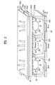
- FIG. 2 is a perspective view illustrating the configuration of discharge cells included in the plasma display panel according to an embodiment of the present invention. Now, the embodiment of the plasma display panel according to the present invention will be described with reference to FIG. 2.
- the plasma display panel according to the present embodiment includes an upper panel and a lower panel, which are arranged to face each other while interposing barrier ribs therebetween.
- the upper panel includes an upper substrate 70 having an image display surface, and sustain electrode pairs arranged on the upper substrate 70, each sustain electrode pair consisting of a pair of transparent electrodes 80a and 80b and a pair of bus electrodes 80a' and 80b'.
- the lower panel includes a lower substrate 10, and address electrodes 20 arranged on the lower substrate 10 to intersect the above described sustain electrode pairs.
- the upper panel and the lower panel are coupled parallel to each other with a predetermined distance therebetween.
- the stripe type or well type barrier ribs 40 are arranged parallel to one another on the lower panel.
- the plurality of address electrodes 20 are arranged parallel to the barrier ribs, to generate vacuum ultraviolet rays by performing an address discharge.
- Red, Green, and Blue phosphors 50a, 50b, and 50c are applied onto an upper surface of the lower panel, to discharge visible rays for displaying an image during the address discharge.
- a lower dielectric layer 30 is formed between the address electrodes 20 and the phosphors 50a, 50b, and 50c, to protect the address electrodes 20.
- An upper dielectric layer 90 is formed on the sustain electrode pairs, and in turn, the first protective layer 100a and the second protective layer 100b are formed on the upper dielectric layer 90 in sequence.
- the detailed characteristics of the first and second protective layers 100a and 100b are as described above.
- the first protective layer 100a which is made of magnesium oxide, etc., protects the upper dielectric layer 90.
- the second protective layer 100b which is in contact with the discharge spaces, is made of magnesium oxide, etc., to achieve an improvement in discharge characteristics as described above.
- FIGs. 3A and 3B are graphs illustrating a surface discharge voltage and an opposed discharge voltage of the plasma display panel according to the present invention.
- FIG. 4A is a graph illustrating the jitter characteristics of the plasma display panel according to the present invention.
- FIG. 4B is a graph illustrating the cathode ray luminescence characteristics of a metallic oxide constituting the protective layer of the plasma display panel according to the present invention.
- a conventional plasma display panel causes a surface discharge at approximately 320 volts, but the plasma display panel according to the present invention causes a surface discharge at 305 volts or less.
- the conventional plasma display panel causes an opposed discharge at approximately 258 volts, but the plasma display panel according to the present invention causes an opposed discharge at 250 volts or less. Accordingly, the present invention has the effect of lowering a discharge start voltage, thereby lowering the consumption of electricity by the plasma display panel.
- Discharge characteristics of the conventional plasma display panel having a film type protective layer and the plasma display panel of the present invention having a metallic oxide type protective layer will be represented in the following Table 2.
- the conventional plasma display panel having a film type protective layer has a discharge delay time of approximately 2 microseconds, but the plasma display panel according to the present invention has a discharge delay time of 1.2 microseconds or less.
- the jitter characteristics of the film type protective layer of the conventional plasma display panel and the metallic oxide type protective layer of the plasma display panel according to the present invention will be represented in the following Table 3.
- the film type protective layer has a slightly faster formative time T f , but other times are more shortened in the metallic oxide type protective layer, resulting in a reduction in the overall discharge delay time of the metallic oxide type protective layer.
- Such an improvement in jitter characteristics is accomplished by the fact that a metallic oxide contained in the second protective layer has a maximum cathode ray luminescence value within a wavelength region of 300 to 500 nanometers.
- the method of the present embodiment is related to the manufacture of the plasma display panel having the above described configuration.
- a first protective layer is deposited on a dielectric layer that was previously formed on an upper panel.
- the first protective layer may be formed by any one method selected from among a spray method, a coating method, a chemical vapor deposition (CVD) method, an electronic beam (E-beam) method, an ion-plating method, a sol-gel method, a sputtering method, and the like.
- the first protective layer is formed close to the dielectric layer, to protect the dielectric layer from shock caused by positive ions, etc.
- the first protective layer preferably has a thickness of 100 to 1,000 nanometers.
- the thickness of the first protective layer is less than 100 nanometers, there is a risk of an erroneous discharge. On the other hand, if the thickness of the first protective layer is more than 1,000 nanometers, it may cause problems in manufacturing processes and costs.
- the first protective layer contains magnesium oxide, and additionally, may contain the above described dopant. If the dopant is added, it has the effect of lowering a jitter value during an address discharge period. However, if the content of the dopant exceeds a predetermined value or more, it may disadvantageously increase the jitter value. Therefore, preferably, the doping of the dopant is performed within a range to reduce the jitter value to the maximum extent, and more preferable, the dopant is contained in the protective layer in an amount of 20 to 500 ppm.
- a first source material as a constituent material of the first protective layer is prepared.
- the first source material consists of magnesium oxide and a slight amount of dopant, and the dopant is selected from the group consisting of Al, Cr, H 2 , Si, Sc and Gd.
- the first source material may be provided as a single source material obtained by doping the above described dopant in magnesium oxide, the magnesium oxide and the dopant may be prepared separately.
- the above described first source material is heated at a high temperature, to deposit the first protective layer on the dielectric layer by use of a physical energy.
- the second protective layer is deposited on the first protective layer by any one method selected from a spray method, a coating method, a chemical vapor deposition (CVD) method, an electronic beam (E-beam) method, an ion-plating method, a sol-gel method, a sputtering method, and the like.
- CVD chemical vapor deposition
- E-beam electronic beam
- ion-plating method a sol-gel method
- a sputtering method and the like.
- the second protective layer has a feature of containing a single-crystal metallic oxide having a maximum cathode ray luminescence value within a wavelength region of 300 to 500 nanometers.
- the metallic oxide is obtained by supplying a gas-phase metallic element with 2 to 20 sccm of oxygen and 0 to 18 sccm of argon.
- a second source material as a constituent material of the second protective layer is prepared.
- the second source material consists of only magnesium oxide.
- the second protective layer is formed on the first protective layer by use of steam generated by heating the second source material.
- the magnesium oxide is deposited to have a single crystal structure.
- the magnesium oxide in the second protective layer has a medium physical property of a layer and a crystal, and can reinforce the deposition strength of the second protective layer as compared to a spray method, etc.
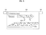
- FIG. 5 is a view illustrating an embodiment of a chemical vapor deposition apparatus according to the present invention.
- the embodiment of the chemical vapor deposition apparatus according to the present invention will be described hereinafter.
- the chemical vapor deposition apparatus includes a chamber, a temperature regulator, and a controller.
- the chamber 200 includes an inlet portion 210 for injecting a source material, etc. into the chamber 200, and an outlet portion 220 for discharging the source material, etc. to the outside.
- the chamber 200 is provided with the temperature regulator for regulating the interior temperature of the chamber 200 and the controller for regulating the flow rates of a carrier gas and a reaction gas within the chamber 200.
- the second protective layer 100b is formed via the chemical vapor deposition method.
- a carrier gas, a reaction gas, a precursor, and a source material are injected into the chamber 200.
- the source material is, for example, metal-alkoxide, to facilitate the growth of magnesium oxide crystals.
- the carrier gas may be nitrogen or hydrogen, and the reaction gas may be any one of oxygen, hydrogen, nitrogen, and argon.
- the second protective layer In a process for forming the second protective layer on the first protective layer, nucleus generation sites are formed on the first protective layer, and a magnesium oxide single crystal is grown from each of the sites. Each magnesium oxide single crystal has an irregular shape, and thus, the overall protective layer has an uneven surface.
- the second protective layer preferably has a thickness of 100 to 1,500 nanometers.
- the flow rates of the carrier gas and the reaction gas are regulated by the controller, and the interior temperature of the chamber is regulated by the temperature regulator.
- the above described second protective layer may be deposited by a liquid phase deposition method, rather than the chemical vapor deposition method.
- the deposition of the second protective layer using the liquid phase deposition method will be described.
- a second protective layer liquid is prepared by pre-mixing a solvent, a dispersant, and a single-crystal metallic oxide powder (S410).
- the metallic oxide may be an alkali or alkaline-earth metallic oxide.
- 1 to 10 wt% of the single-crystal metallic oxide powder is mixed with 90 to 99 wt% of the solvent and the dispersant.
- the solvent may be an alcohol, glycol or diol, propylene glycol ether, propylene glycol acetate, ketone, butyl carbitol acetate (BCA), xylene, terpineol, texanol, water, or a mixture thereof.
- the dispersant may be acryl, epoxy, urethane, acrylic urethane, alkyd, poly amid polymer, poly carboxylic acid, or a mixture thereof.
- the prepared second protective layer liquid is subjected to a milling process (S420).
- the milling of the second protective layer liquid is performed by a milling machine.
- the preparation of the second protective layer liquid is continued for 1 to 10 minutes at 2,000 to 4,000 rpm.
- the milling of the second protective layer liquid is continued for 10 to 60 minutes at 6,000 to 10,000 rpm.
- the solvent, the dispersant, and the single-crystal metallic oxide powder are mixed by stirring for a predetermined time (for example, for an hour), and are subjected to an ultrasonic distribution using an ultrasonic distributor, to thereby form the second protective layer liquid.
- the milled second protective layer liquid is applied onto the overall surface of the first protective layer by any one method selected from a spray coating method, a bar coating method, a screen printing method, and a green sheet method (S430). Thereafter, the second protective layer liquid, applied onto the first protective layer, is dried and fired (S440), to form the second protective layer (S450).
- the drying is performed at a temperature of 100 to 200 degrees centigrade, and the firing is performed at a temperature of 400 to 600 degrees centigrade. Thereby, particles including the single-crystal metallic oxide powder remain irregularly, in the form of lumps, on the overall surface of the first protective layer, to form the second protective layer.
- a solvent, a dispersant, and a single-crystal magnesium oxide (MgO) nano-powder are pre-mixed, to prepare a second protective layer liquid (S410).
- a solvent may be an alcohol, glycol or diol, propylene glycol ether, propylene glycol acetate, ketone, butyl carbitol acetate (BCA), xylene, terpineol, texanol, water, or a mixture thereof.
- the dispersant may be acryl, epoxy, urethane, acrylic urethane, alkyd, poly amid polymer, poly carboxylic acid, or a mixture thereof.
- the solvent, the dispersant, and the single-crystal magnesium oxide nano-powder are mixed by stirring for a predetermined time (for example, for an hour), and are subjected to an ultrasonic dispersion using an ultrasonic distributor, to thereby form the second protective layer liquid.
- the second protective layer liquid is subjected to a milling process (S420).
- the milling of the second protective layer liquid is performed by a milling machine.
- the milled second protective layer liquid is applied onto the first protective layer by any one method selected from a screen printing method, a dispensing method, a photolithography method, and an ink-jet method (S430).
- the second protective layer liquid, applied onto the first protective layer, is dried and fired (S440), to form the second protective layer (S450).
- the drying is performed at a temperature of 100 to 200 degrees centigrade, and the firing is performed at a temperature of 400 to 600 degrees centigrade.
- particles including the single-crystal metallic oxide nano-powder remain, in the form of lumps, on predetermined positions of the first protective layer, to form the second protective layer.
- two transparent electrodes are formed on the upper substrate, and in turn, bus electrodes as auxiliary electrodes are deposited on certain positions of the respective electrodes, to form discharge cell sustain electrodes.
- an upper dielectric layer is formed over the above electrodes, and in turn, a first protective layer and a second protective layer are formed on the dielectric layer in sequence.
- the manufacture of a lower substrate comprises an operation for forming address electrodes on a glass substrate, an operation for forming a lower dielectric layer for the protection of the address electrodes, an operation for forming barrier ribs on an upper surface of the lower dielectric layer to divide discharge cells from one another, and an operation for forming a phosphor layer between the barrier ribs for discharging visible rays required for the display of an image.
- a sealing material is applied onto the lower substrate formed with the address electrodes, to bond the lower substrate to the upper substrate. In this way, the manufacture of the plasma display panel is completed.
Landscapes
- Engineering & Computer Science (AREA)
- Physics & Mathematics (AREA)
- Plasma & Fusion (AREA)
- Manufacturing & Machinery (AREA)
- Gas-Filled Discharge Tubes (AREA)
Applications Claiming Priority (3)
| Application Number | Priority Date | Filing Date | Title |
|---|---|---|---|
| KR20060071600 | 2006-07-28 | ||
| KR20060071601 | 2006-07-28 | ||
| KR1020070008805A KR20080070919A (ko) | 2007-01-29 | 2007-01-29 | 화학 기상 증착 장치, 이를 이용한 플라즈마 디스플레이패널 및 그 제조방법 |
Publications (2)
| Publication Number | Publication Date |
|---|---|
| EP1883092A2 true EP1883092A2 (fr) | 2008-01-30 |
| EP1883092A3 EP1883092A3 (fr) | 2009-08-05 |
Family
ID=38728909
Family Applications (1)
| Application Number | Title | Priority Date | Filing Date |
|---|---|---|---|
| EP07252827A Withdrawn EP1883092A3 (fr) | 2006-07-28 | 2007-07-17 | Panneau d'affichage à plasma et son procédé de fabrication |
Country Status (3)
| Country | Link |
|---|---|
| US (1) | US20080024062A1 (fr) |
| EP (1) | EP1883092A3 (fr) |
| JP (1) | JP2008034390A (fr) |
Cited By (12)
| Publication number | Priority date | Publication date | Assignee | Title |
|---|---|---|---|---|
| EP2139018A4 (fr) * | 2008-03-12 | 2010-04-28 | Panasonic Corp | Procédé de fabrication de panneau d'affichage à plasma |
| EP2136386A4 (fr) * | 2008-03-12 | 2010-04-28 | Panasonic Corp | Procédé de fabrication d'écran plasma |
| EP2136387A4 (fr) * | 2008-03-06 | 2010-04-28 | Panasonic Corp | Dispositif d'affichage à plasma |
| EP2163521A3 (fr) * | 2008-09-05 | 2010-06-30 | Samsung SDI Co., Ltd. | Matériau pour la formation d'une couche de protection, procédé pour la préparation du matériau et PDP comprenant la couche de protection |
| EP2031631A3 (fr) * | 2007-09-03 | 2010-09-01 | Samsung SDI Co., Ltd. | Couche de protection comprenant une couche d'oxyde de magnésium et matériau de promotion de l'émission d'électrons, leur procédé de préparation, et panneau d'affichage à plasma les comprenant |
| EP2136384A4 (fr) * | 2008-04-04 | 2010-12-08 | Panasonic Corp | Procédé de fabrication de panneau d'affichage à plasma |
| CN101996835A (zh) * | 2009-08-19 | 2011-03-30 | 三星Sdi株式会社 | 等离子体显示面板 |
| EP2136349A4 (fr) * | 2008-03-10 | 2011-04-20 | Panasonic Corp | Dispositif d'affichage à plasma |
| EP2338850A1 (fr) * | 2009-09-29 | 2011-06-29 | Samsung SDI Co., Ltd. | Zusammensetzung für eine Schutzschicht einer Plasmaanzeigetafel, Plasamanzeigetafel und Herstellungsverfahren dafür |
| EP2146365A4 (fr) * | 2008-04-09 | 2011-07-27 | Panasonic Corp | Procédé pour la fabrication d'écran à plasma |
| EP2184758A4 (fr) * | 2008-06-26 | 2011-08-03 | Panasonic Corp | Procédé de production d'un panneau d'affichage plasma |
| EP2184759A4 (fr) * | 2008-07-01 | 2011-10-26 | Panasonic Corp | Procédé de fabrication d'un panneau d'affichage à plasma |
Families Citing this family (13)
| Publication number | Priority date | Publication date | Assignee | Title |
|---|---|---|---|---|
| CN101779264B (zh) * | 2007-08-10 | 2012-05-09 | 株式会社日立制作所 | 等离子体显示面板 |
| JP2009170192A (ja) * | 2008-01-15 | 2009-07-30 | Panasonic Corp | プラズマディスプレイパネル |
| JP4961495B2 (ja) * | 2008-03-05 | 2012-06-27 | 株式会社日立製作所 | プラズマディスプレイパネルの製造方法、酸化マグネシウム結晶体粉体の製造方法 |
| JP2009218023A (ja) * | 2008-03-10 | 2009-09-24 | Panasonic Corp | プラズマディスプレイパネル |
| JP2009218133A (ja) * | 2008-03-12 | 2009-09-24 | Panasonic Corp | プラズマディスプレイパネルの製造方法 |
| JP2009252482A (ja) * | 2008-04-04 | 2009-10-29 | Panasonic Corp | プラズマディスプレイパネル |
| JP2009253790A (ja) * | 2008-04-09 | 2009-10-29 | Panasonic Corp | 操作記録同時再生システム |
| JP4566249B2 (ja) * | 2008-04-11 | 2010-10-20 | 株式会社日立製作所 | プラズマディスプレイパネルおよびその製造方法 |
| JP4589980B2 (ja) * | 2008-06-04 | 2010-12-01 | パナソニック株式会社 | プラズマディスプレイパネルの製造方法 |
| JP5012698B2 (ja) * | 2008-06-30 | 2012-08-29 | パナソニック株式会社 | プラズマディスプレイパネル用金属酸化物ペースト及びプラズマディスプレイパネルの製造方法 |
| JP2010140837A (ja) * | 2008-12-15 | 2010-06-24 | Panasonic Corp | プラズマディスプレイパネル |
| KR101076802B1 (ko) * | 2009-06-05 | 2011-10-25 | 삼성에스디아이 주식회사 | 보호층 재료 및 이를 이용하여 형성한 보호층을 구비하는 플라즈마 디스플레이 패널 |
| JPWO2011099266A1 (ja) * | 2010-02-12 | 2013-06-13 | パナソニック株式会社 | プラズマディスプレイパネルの製造方法 |
Family Cites Families (9)
| Publication number | Priority date | Publication date | Assignee | Title |
|---|---|---|---|---|
| US6307319B1 (en) * | 1999-12-28 | 2001-10-23 | Samsung Sdi Co., Ltd. | Plasma display panel and method for manufacturing the same |
| JP4153983B2 (ja) * | 2000-07-17 | 2008-09-24 | パイオニア株式会社 | 保護膜、その成膜方法、プラズマディスプレイパネル及びその製造方法 |
| JP4357778B2 (ja) * | 2001-11-22 | 2009-11-04 | パナソニック株式会社 | Ac型プラズマディスプレイパネルの駆動方法 |
| JP4195279B2 (ja) * | 2002-12-02 | 2008-12-10 | 宇部マテリアルズ株式会社 | 高純度酸化マグネシウム微粉末の製造方法 |
| JP4611207B2 (ja) * | 2003-11-10 | 2011-01-12 | パナソニック株式会社 | プラズマディスプレイパネル |
| JP4636857B2 (ja) * | 2004-05-06 | 2011-02-23 | パナソニック株式会社 | プラズマディスプレイ装置 |
| JP4683547B2 (ja) * | 2004-09-16 | 2011-05-18 | パナソニック株式会社 | プラズマディスプレイパネル |
| JP4541840B2 (ja) * | 2004-11-08 | 2010-09-08 | パナソニック株式会社 | プラズマディスプレイパネル |
| US7713639B2 (en) * | 2004-12-17 | 2010-05-11 | Samsung Sdi Co., Ltd. | Protective layer, composite for forming the protective layer, method of forming the protective layer, and plasma display panel including the protective layer |
-
2007
- 2007-07-17 EP EP07252827A patent/EP1883092A3/fr not_active Withdrawn
- 2007-07-27 JP JP2007195970A patent/JP2008034390A/ja not_active Withdrawn
- 2007-07-30 US US11/830,404 patent/US20080024062A1/en not_active Abandoned
Cited By (16)
| Publication number | Priority date | Publication date | Assignee | Title |
|---|---|---|---|---|
| EP2031631A3 (fr) * | 2007-09-03 | 2010-09-01 | Samsung SDI Co., Ltd. | Couche de protection comprenant une couche d'oxyde de magnésium et matériau de promotion de l'émission d'électrons, leur procédé de préparation, et panneau d'affichage à plasma les comprenant |
| EP2136387A4 (fr) * | 2008-03-06 | 2010-04-28 | Panasonic Corp | Dispositif d'affichage à plasma |
| EP2136349A4 (fr) * | 2008-03-10 | 2011-04-20 | Panasonic Corp | Dispositif d'affichage à plasma |
| EP2136386A4 (fr) * | 2008-03-12 | 2010-04-28 | Panasonic Corp | Procédé de fabrication d'écran plasma |
| EP2139018A4 (fr) * | 2008-03-12 | 2010-04-28 | Panasonic Corp | Procédé de fabrication de panneau d'affichage à plasma |
| EP2136384A4 (fr) * | 2008-04-04 | 2010-12-08 | Panasonic Corp | Procédé de fabrication de panneau d'affichage à plasma |
| EP2146365A4 (fr) * | 2008-04-09 | 2011-07-27 | Panasonic Corp | Procédé pour la fabrication d'écran à plasma |
| EP2184758A4 (fr) * | 2008-06-26 | 2011-08-03 | Panasonic Corp | Procédé de production d'un panneau d'affichage plasma |
| EP2184759A4 (fr) * | 2008-07-01 | 2011-10-26 | Panasonic Corp | Procédé de fabrication d'un panneau d'affichage à plasma |
| US7977883B2 (en) | 2008-09-05 | 2011-07-12 | Samsung Sdi Co., Ltd. | Plasma display panel comprising magnesium oxide protective layer |
| EP2163521A3 (fr) * | 2008-09-05 | 2010-06-30 | Samsung SDI Co., Ltd. | Matériau pour la formation d'une couche de protection, procédé pour la préparation du matériau et PDP comprenant la couche de protection |
| EP2287881A3 (fr) * | 2009-08-19 | 2011-05-18 | Samsung SDI Co., Ltd. | Panneau d'affichage à plasma |
| CN101996835A (zh) * | 2009-08-19 | 2011-03-30 | 三星Sdi株式会社 | 等离子体显示面板 |
| US8058805B2 (en) | 2009-08-19 | 2011-11-15 | Samsung Sdi Co., Ltd. | Plasma display panel |
| EP2338850A1 (fr) * | 2009-09-29 | 2011-06-29 | Samsung SDI Co., Ltd. | Zusammensetzung für eine Schutzschicht einer Plasmaanzeigetafel, Plasamanzeigetafel und Herstellungsverfahren dafür |
| KR101107107B1 (ko) * | 2009-09-29 | 2012-01-30 | 삼성에스디아이 주식회사 | 플라즈마 디스플레이 패널의 보호막용 조성물 및 플라즈마 디스플레이 패널 |
Also Published As
| Publication number | Publication date |
|---|---|
| JP2008034390A (ja) | 2008-02-14 |
| EP1883092A3 (fr) | 2009-08-05 |
| US20080024062A1 (en) | 2008-01-31 |
Similar Documents
| Publication | Publication Date | Title |
|---|---|---|
| EP1883092A2 (fr) | Panneau d'affichage à plasma et son procédé de fabrication | |
| EP1267383B1 (fr) | Ecran plat à plasma et procédé de production | |
| JP4505474B2 (ja) | プラズマディスプレイパネル | |
| US8030834B2 (en) | Flat display device, plasma device panel and field emission containing phosphor coated with a heat-resistant material | |
| JP3331907B2 (ja) | プラズマディスプレイパネルおよびその製造方法 | |
| JP2004323576A (ja) | 蛍光体およびプラズマディスプレイ装置 | |
| CN100372042C (zh) | 等离子体显示屏及其制造方法 | |
| JP3425063B2 (ja) | プラズマディスプレイパネル及びその製造方法 | |
| KR19990073478A (ko) | 교류구동형플라즈마표시소자용유전체칼라필터및그제조방법 | |
| KR100992730B1 (ko) | 플라즈마 디스플레이 패널 | |
| JP2005063931A (ja) | プラズマディスプレイパネルの前面基板及びその製造方法 | |
| JP2000087030A (ja) | プラズマディスプレイパネル用蛍光体及び蛍光体インキ | |
| CN101563748B (zh) | 等离子体显示面板及其制造方法 | |
| EP1777318A1 (fr) | MATERIAU DE DEPOSITION DE MgO | |
| US20070194686A1 (en) | Phosphor, phosphor paste composition including the same, and flat display device including phosphor layer including the phosphor | |
| KR20020038960A (ko) | 형광체의 제조방법, 플라즈마 디스플레이 패널 표시장치및 형광등 | |
| JPH10269952A (ja) | プラズマディスプレイパネルおよびプラズマディスプレイ用蛍光体の製造方法 | |
| KR100524777B1 (ko) | 플라즈마 디스플레이 패널 제조 방법 | |
| US6903507B2 (en) | Plasma display panel and its manufacturing method | |
| JP2000156165A (ja) | プラズマディスプレイパネルの製造方法 | |
| JP3988515B2 (ja) | プラズマディスプレイパネルおよびその製造方法 | |
| CN100454476C (zh) | 等离子体显示装置及其制造方法 | |
| JP3234567B2 (ja) | プラズマディスプレイパネルの製造方法 | |
| WO2011138870A1 (fr) | Panneau d'affichage à plasma | |
| JP2009301841A (ja) | プラズマディスプレイパネル |
Legal Events
| Date | Code | Title | Description |
|---|---|---|---|
| PUAI | Public reference made under article 153(3) epc to a published international application that has entered the european phase |
Free format text: ORIGINAL CODE: 0009012 |
|
| AK | Designated contracting states |
Kind code of ref document: A2 Designated state(s): AT BE BG CH CY CZ DE DK EE ES FI FR GB GR HU IE IS IT LI LT LU LV MC MT NL PL PT RO SE SI SK TR |
|
| AX | Request for extension of the european patent |
Extension state: AL BA HR MK YU |
|
| 17P | Request for examination filed |
Effective date: 20080626 |
|
| PUAL | Search report despatched |
Free format text: ORIGINAL CODE: 0009013 |
|
| AK | Designated contracting states |
Kind code of ref document: A3 Designated state(s): AT BE BG CH CY CZ DE DK EE ES FI FR GB GR HU IE IS IT LI LT LU LV MC MT NL PL PT RO SE SI SK TR |
|
| AX | Request for extension of the european patent |
Extension state: AL BA HR MK RS |
|
| AKX | Designation fees paid |
Designated state(s): DE FR GB NL |
|
| STAA | Information on the status of an ep patent application or granted ep patent |
Free format text: STATUS: THE APPLICATION IS DEEMED TO BE WITHDRAWN |
|
| 18D | Application deemed to be withdrawn |
Effective date: 20100202 |