EP1883102A2 - Verfahren zur Verbesserung der Qualität eines SiC-Kristalls und ein SiC-Halbleiterbauelement. - Google Patents
Verfahren zur Verbesserung der Qualität eines SiC-Kristalls und ein SiC-Halbleiterbauelement. Download PDFInfo
- Publication number
- EP1883102A2 EP1883102A2 EP06255833A EP06255833A EP1883102A2 EP 1883102 A2 EP1883102 A2 EP 1883102A2 EP 06255833 A EP06255833 A EP 06255833A EP 06255833 A EP06255833 A EP 06255833A EP 1883102 A2 EP1883102 A2 EP 1883102A2
- Authority
- EP
- European Patent Office
- Prior art keywords
- layer
- sic
- type
- carbon
- atoms
- Prior art date
- Legal status (The legal status is an assumption and is not a legal conclusion. Google has not performed a legal analysis and makes no representation as to the accuracy of the status listed.)
- Granted
Links
Images


Classifications
-
- H—ELECTRICITY
- H10—SEMICONDUCTOR DEVICES; ELECTRIC SOLID-STATE DEVICES NOT OTHERWISE PROVIDED FOR
- H10D—INORGANIC ELECTRIC SEMICONDUCTOR DEVICES
- H10D84/00—Integrated devices formed in or on semiconductor substrates that comprise only semiconducting layers, e.g. on Si wafers or on GaAs-on-Si wafers
- H10D84/01—Manufacture or treatment
-
- C—CHEMISTRY; METALLURGY
- C30—CRYSTAL GROWTH
- C30B—SINGLE-CRYSTAL GROWTH; UNIDIRECTIONAL SOLIDIFICATION OF EUTECTIC MATERIAL OR UNIDIRECTIONAL DEMIXING OF EUTECTOID MATERIAL; REFINING BY ZONE-MELTING OF MATERIAL; PRODUCTION OF A HOMOGENEOUS POLYCRYSTALLINE MATERIAL WITH DEFINED STRUCTURE; SINGLE CRYSTALS OR HOMOGENEOUS POLYCRYSTALLINE MATERIAL WITH DEFINED STRUCTURE; AFTER-TREATMENT OF SINGLE CRYSTALS OR A HOMOGENEOUS POLYCRYSTALLINE MATERIAL WITH DEFINED STRUCTURE; APPARATUS THEREFOR
- C30B29/00—Single crystals or homogeneous polycrystalline material with defined structure characterised by the material or by their shape
- C30B29/10—Inorganic compounds or compositions
- C30B29/36—Carbides
-
- C—CHEMISTRY; METALLURGY
- C30—CRYSTAL GROWTH
- C30B—SINGLE-CRYSTAL GROWTH; UNIDIRECTIONAL SOLIDIFICATION OF EUTECTIC MATERIAL OR UNIDIRECTIONAL DEMIXING OF EUTECTOID MATERIAL; REFINING BY ZONE-MELTING OF MATERIAL; PRODUCTION OF A HOMOGENEOUS POLYCRYSTALLINE MATERIAL WITH DEFINED STRUCTURE; SINGLE CRYSTALS OR HOMOGENEOUS POLYCRYSTALLINE MATERIAL WITH DEFINED STRUCTURE; AFTER-TREATMENT OF SINGLE CRYSTALS OR A HOMOGENEOUS POLYCRYSTALLINE MATERIAL WITH DEFINED STRUCTURE; APPARATUS THEREFOR
- C30B31/00—Diffusion or doping processes for single crystals or homogeneous polycrystalline material with defined structure; Apparatus therefor
- C30B31/20—Doping by irradiation with electromagnetic waves or by particle radiation
- C30B31/22—Doping by irradiation with electromagnetic waves or by particle radiation by ion-implantation
-
- H—ELECTRICITY
- H10—SEMICONDUCTOR DEVICES; ELECTRIC SOLID-STATE DEVICES NOT OTHERWISE PROVIDED FOR
- H10D—INORGANIC ELECTRIC SEMICONDUCTOR DEVICES
- H10D10/00—Bipolar junction transistors [BJT]
- H10D10/40—Vertical BJTs
- H10D10/441—Vertical BJTs having an emitter-base junction ending at a main surface of the body and a base-collector junction ending at a lateral surface of the body
-
- H—ELECTRICITY
- H10—SEMICONDUCTOR DEVICES; ELECTRIC SOLID-STATE DEVICES NOT OTHERWISE PROVIDED FOR
- H10D—INORGANIC ELECTRIC SEMICONDUCTOR DEVICES
- H10D12/00—Bipolar devices controlled by the field effect, e.g. insulated-gate bipolar transistors [IGBT]
- H10D12/411—Insulated-gate bipolar transistors [IGBT]
- H10D12/441—Vertical IGBTs
-
- H—ELECTRICITY
- H10—SEMICONDUCTOR DEVICES; ELECTRIC SOLID-STATE DEVICES NOT OTHERWISE PROVIDED FOR
- H10D—INORGANIC ELECTRIC SEMICONDUCTOR DEVICES
- H10D62/00—Semiconductor bodies, or regions thereof, of devices having potential barriers
- H10D62/80—Semiconductor bodies, or regions thereof, of devices having potential barriers characterised by the materials
- H10D62/83—Semiconductor bodies, or regions thereof, of devices having potential barriers characterised by the materials being Group IV materials, e.g. B-doped Si or undoped Ge
- H10D62/832—Semiconductor bodies, or regions thereof, of devices having potential barriers characterised by the materials being Group IV materials, e.g. B-doped Si or undoped Ge being Group IV materials comprising two or more elements, e.g. SiGe
- H10D62/8325—Silicon carbide
-
- H—ELECTRICITY
- H10—SEMICONDUCTOR DEVICES; ELECTRIC SOLID-STATE DEVICES NOT OTHERWISE PROVIDED FOR
- H10P—GENERIC PROCESSES OR APPARATUS FOR THE MANUFACTURE OR TREATMENT OF DEVICES COVERED BY CLASS H10
- H10P36/00—Gettering within semiconductor bodies
Definitions
- the present invention relates to a method for improving the quality of a crystal layer of SiC after the growth thereof.
- This invention also relates to a semiconductor device produced by carrying out such a method.
- Fig. 19 is a schematic view showing the atomic arrangement of Si and C in the perfect 4H-SiC crystal.
- the crystal lattices of semiconductors are not perfect even in the case where they do not contain any impurities, some amount of vacancies and interstitials is always present to maintain the thermodynamic equilibrium.
- the point defects in a compound semiconductor can be classified as follows:
- the shallow level centers are usually donor or acceptor impurities.
- deep level defects interact with both the conduction band and valence band and can be very efficient as centers of carrier trapping and recombination. In such a case, these defects are called electrically active and often referred as "traps". They can influence carrier lifetime significantly even at very low concentrations.
- SiC layers of excellent quality are available at present, they still contain native intrinsic defects which act as carrier traps and degrade materials characteristics.
- an intrinsic defect concentration is increased as a growth rate and a growth temperature are increased.
- the high thermal stability of SiC makes it usually difficult or impossible to remove these defects by a thermal treatment (anneal out). Since the increased growth rate is necessary for growing thick layers which are cost-effective, it is important to find a way to achieve low defect density in these layers.
- defect concentration can be reduced, and the quality of a material in the state that crystal growth is completed (hereafter referred to as-grown material) can be improved to a certain level by a high temperature thermal treatment (annealing).
- annealing a high temperature thermal treatment
- the improvement is not sufficient due to the above described high thermal stability.
- a part of intrinsic defects created by irradiation of electrons, protons, or ions can be removed by annealing, but another part is just reduced, and the lowest defect concentration is usually determined by the original as-grown material.
- Non Patent Document 1 The electrically active defects in an as-grown SiC layer have been investigated by Zhang and others (Non Patent Document 1).
- the major electron traps and hole traps in an as-grown SiC layer were determined by using the Deep Level Transient Spectroscopy (DLTS) and the Minority Carrier Transient Spectroscopy (MCTS). More specifically, the traps in relation to the Ti and B impurities, and the Z1/Z2 and EH6/7 intrinsic defects in relation to electron traps were measured by these methods. In addition, the Z1/Z2 and EH6/7 traps showed the inverse correlation with the minority carrier lifetime.
- DLTS Deep Level Transient Spectroscopy
- MCTS Minority Carrier Transient Spectroscopy
- Non Patent Document 2 Klein and others concluded that the Z1/Z2 defects have a large capture cross section for holes and dominate in limiting the minority carrier lifetime in the n-type SiC layer.
- Non Patent Document 4 Storasta and others investigated the deep level in relation to the selective displacement of carbon atoms (Non Patent Document 4).
- the irradiation with electrons of energy below the threshold for silicon atom displacement was enough to create the Z1/Z2 and EH6/7 intrinsic defects. Consequently, they concluded that they must have relation to defects (complexes) related to either of carbon vacancies and interstitials.
- Patent Document 1 relates to the technique for forming a p-type layer of boron that is utilized as a device structure.
- boron and carbon atoms are ion-implanted simultaneously into the surface layer, and electrically activated boron atoms are selectively introduced not into the carbon vacancies but into the silicon vacancies due to the existence of excess carbon interstitials in the surface layer in the case where boron atoms compete with silicon interstitials and carbon interstitials in the surface layer during annealing.
- the object of such a technique already known is to make the impurities that have been implanted into the surface layer for forming the device structure, to be electrically active in the surface layer by annealing.
- the above described technique does not indicate that carbon interstitials are introduced into the shallow surface layer of the as-grown SiC crystal, the carbon interstitials are diffused into a region deeper than the surface layer by the subsequent annealing, and the point defects vanish in the deep portion of the wafer.
- An object of the present invention is to provide a method of effectively reducing or eliminating the carrier trapping centers by high temperature annealing. Moreover, another object of the present invention is to provide an SiC semiconductor device with less carrier trapping centers.
- the object of the present invention is achieved by the method comprising the additional steps of:
- This technique results in additional carbon interstitials available which diffuse into the material underneath the implanted layer during the annealing step (b). These excess carbon interstitials fill the vacancies during the annealing step (b), thus eliminating them or forming other defects which are not act as excellent recombination centers. In this way, it is possible to improve the carrier lifetime in the SiC layer which is important for bipolar devices.
- carbon that can introduce carbon interstitials directly and that acts neutrally to the SiC crystal is most preferable to use carbon that can introduce carbon interstitials directly and that acts neutrally to the SiC crystal as an atom to be implanted into the surface layer in order to introduce excess carbon interstitials and to fill the vacancies in SiC crystal layer.
- carbon atoms that constitute an SiC crystal can be knocked out from the site by implanted atoms, and as a result (indirectly), carbon interstitials can be created in the surface layer of the SiC crystal.
- silicon atoms, hydrogen atoms, and helium atoms are neutral in the SiC crystal similarly to carbon atoms, p-type or n-type doping into the surface layer can be prevented from being carried out by a high temperature annealing after carbon interstitials are introduced. Consequently, those atoms are more suitable than other atoms.
- those implanted atoms act as an impurity (dopant) of a p-type or an n-type, and the surface layer shows a p-type or an n-type of a high concentration or a high resistance after annealing. Meanwhile, in a region deeper than the surface layer, carbon interstitials are diffused out from the surface layer by a high temperature annealing, thereby enabling to reduce vacancies.
- the carbon interstitials can also be introduced into the surface layer. This is because, in the case where an electron beam is irradiated to the SiC crystal and energy of the electron beam is approximately 90 KeV or higher, carbon atoms that constitute an SiC crystal are knocked out from the original site and carbon interstitials are created.
- the carbon interstitials into the surface layer by oxidation of the surface layer in the SiC crystal in an oxygen atmosphere at 800°C or higher. This is because, in the case where the surface layer of the SiC crystal is oxidized, excess carbon interstitials are created mainly around an interface of the oxidized layer and the SiC crystal. In such a case, the surface layer in the SiC crystal cannot be oxidized with a sufficient speed at a temperature less than 800°C.
- the most suitable oxidation temperature is in the range from 1050°C to 1250°C.
- a method for improving the quality of an SiC crystal by eliminating or extremely reducing carrier trapping centers in an as-grown SiC crystal layer comprising the steps of:
- An embodiment of the present invention further comprises the step (c) of etching or mechanically removing the surface layer into which atoms have been implanted.
- the step (a) is carried out in the condition that n-type or p-type doping into the surface layer is not carried out by ion-implanting atoms selected from carbon atoms, silicon atoms, hydrogen atoms, or helium atoms in particular.
- the steps (a) and (b) are carried out simultaneously.
- the step (a) is carried out by irradiating an electron beam having energy of 90 KeV or higher.
- the step (a) is carried out by oxidizing the surface layer in an oxygen atmosphere at 800°C or higher.
- the step (a) further comprises selecting the dose of atoms to be implanted in such a manner that a concentration of the created carbon interstitials exceeds that of the electrically active point defects in the bulk layer.
- the ion implantation energy of atoms is in the range from 10 KeV to 10 MeV in the step (a).
- a temperature of the SiC substrate during ion implantation is preferably in the range from 10°C to 1700°C, and more preferably in the range from 20°C to 1000°C.
- an annealing temperature is preferably in the range from 1200 to 2200°C, and more preferably in the range from 1400°C to 1900°C.
- an SiC wafer provided with an epitaxial layer is used in the steps (a) and (b).
- an SiC bulk crystal is used in the steps (a) and (b).
- a wafer sliced from an SiC bulk crystal is used in the steps (a) and (b).
- an SiC monocrystal wafer is used in the steps (a) and (b) that has been formed as an epitaxial layer by a process in which after an SiC epitaxial layer is obtained using a wafer sliced from an SiC bulk crystal as a substrate, the substrate portion is removed.
- an SiC wafer having a combination of any of n-type and p-type epitaxial layers is used in the steps (a) and (b).
- a method for improving the quality of an SiC crystal by eliminating or reducing carrier trapping centers in an as-grown SiC crystal layer comprising the steps of:
- the step (a) further comprises selecting the dose of atoms to be implanted in such a manner that a concentration of the additionally introduced carbon interstitials exceeds that of the electrically active point defects in the grown layer.
- the ion implantation energy of atoms is in the range from 10 KeV to 10 MeV in the step (a).
- a temperature of the SiC substrate during ion implantation is preferably in the range from 10°C to 1700°C, and more preferably in the range from 20°C to 1000°C.
- an SiC wafer provided with an epitaxial layer is used in the steps (a) and (b).
- an SiC bulk crystal is used in the steps (a) and (b).
- a wafer sliced from an SiC bulk crystal is used in the steps (a) and (b).
- an SiC monocrystal wafer is used in the steps (a) and (b) that has been formed as an epitaxial layer by a process in which after an SiC epitaxial layer is obtained using a wafer sliced from an SiC bulk crystal as a substrate, the substrate portion is removed.
- an SiC wafer having a combination of any of n-type and p-type epitaxial layers is used in the steps (a) and (b).
- a width of the shallow surface layer into which the carbon interstitials are introduced by ion implantation or the like in the step (a) is, for instance, in the range from 100 nm to 2000 nm from the surface.
- a width of the region including carbon atoms that have been diffused out by annealing in the step (b) and that have made the electrically active point defects inactive is, for instance, in the range from 10000 nm to 300000 nm from the surface (edge face of the wafer) (10 ⁇ m to 300 ⁇ m from the surface).
- step (a) of the invention other than carbon interstitials, carbon vacancies, silicon vacancies, and silicon interstitials are simultaneously created by carrying out ion implantation into the surface layer. A part of these carbon vacancies, silicon vacancies, and silicon interstitials are diffused into the bulk layer from the surface layer as well as the carbon interstitials in the step (b).
- a carrier lifetime in the bulk layer may be controlled due to a point defect density of the carbon vacancies and complex defects thereof, while in another case, the carrier lifetime in the bulk layer may be controlled due to a point defect density of carbon interstitials and complex defects thereof, silicon interstitials and complex defects thereof, or silicon vacancies and complex defects thereof.
- quality of the bulk layer can be improve d by introducing excess carbon interstitials in the step (a), and combining the carbon interstitials diffused from the surface layer with the carbon vacancies in the bulk layer in the following step (b).
- the effect becomes to dominate by introducing excess carbon vacancies, silicon vacancies, and si licon interstitials in the step (a), and combining the carbon vaca ncies diffused from the surface layer with the carbon interstitial s and complex defects thereof in the bulk layer, the silicon vacan cies diffused from the surface layer with the silicon interstitial s and complex defects thereof in the bulk layer, and the silicon i nterstitials diffused from the surface layer with the silicon vaca ncies and complex defects thereof in the bulk layer in the followi ng step (b).
- a degree of the effect is thought to be dependent on t he crystal quality of the original bulk layer.
- a large stress will be induced in the SiC monocrystal by carrying out ion implantation into the surface layer in the step (a).
- point defects that have been present in the bulk layer such as carbon interstitials, carbon vacancies, silicon interstitials, and silicon vacancies will migrate into the surface layer to relax the stress by carrying the thermal treatment in the step (b), thus the densities of the carbon interstitials and complex defects thereof, the carbon vacancies and complex defects thereof, the silicon interstitials and complex defects thereof, and the silicon vacancies and complex defects thereof that have been present in the bulk layer are reduced.
- a method for improving the quality of an SiC crystal by eliminating or reducing carrier trapping centers in as-grown SiC crystal layer comprising the steps of:
- a semiconductor device of all types including a diode, a transistor, an insulated gate bipolar transistor (IGBT), a metal oxide semiconductor field effect transistor (MOSFET), and a thyristor (including a gate turn-off thyristor), produced using the above described method.
- a bipolar type SiC semiconductor device as described below.
- a carbon implanted layer, a silicon implanted layer, a hydrogen implanted layer, or a helium implanted layer is formed selectively in a region in which a reduction of electrically active point defects is particularly effective in the device.
- Such a carbon implanted layer, a silicon implanted layer, a hydrogen implanted layer, or a helium implanted layer is formed by applying the above method in the fabrication process of the device, and defined by the existence of carbon atoms, silicon atoms, hydrogen atoms, or helium atoms that have been introduced by carrying out ion implantation.
- a carbon implanted layer, a silicon implanted layer, a hydrogen implanted layer, or a helium implanted layer is formed in a region other than that around a p-n interface in which an injection of minority carriers is carried out (within 500 nm from the p-n interface) and that in a conductivity modulation layer.
- such a bipolar type SiC semiconductor device comprises a region in which electrically active point defects are reduced by diffusing out carbon interstitials, silicon interstitials, carbon vacancies or silicon vacancies that have been introduced by the ion implantation of carbon atoms, silicon atoms, hydrogen atoms, or helium atoms into the conductivity modulation layer by annealing, and by combining the carbon interstitials, the silicon interstitials, the carbon vacancies or the silicon vacancies with point defects in the conductivity modulation layer, or a region in which electrically active point defects are reduced by migrating the point defects in the conductivity modulation layer towards the carbon implanted layer, the silicon implanted layer, the hydrogen implanted layer, or the helium implanted layer with annealing by utilizing a stress that have been induced by the ion implantation of carbon atoms, silicon atoms, hydrogen atoms, or helium atoms.
- the bipolar type SiC semiconductor device comprises a region in which point defects are reduced by diffusing out the carbon interstitials that have been introduced by the ion implantation of carbon atoms, silicon atoms, hydrogen atoms, or helium atoms by annealing, and by combining the carbon interstitials and point defects in the conductivity modulation layer (hereafter referred to as carbon diffused region).
- a bipolar type semiconductor device of high withstand voltage in order to restrict an amount of minority carriers to be injected to the conductivity modulation layer (base layer), electron beams or hydrogen ions (protons) are irradiated to a region around a p-n junction interface from which an injection of minority carriers is carried out to the base layer and a region in the conductivity modulation layer in some cases to intentionally increase a concentration of point defects around a p-n junction interface and in the conductivity modulation layer.
- a region within approximately 500 nm from the p-n junction interface influences a degree of an injection amount of minority carriers.
- an object of the present invention is to reduce or eliminate point defects around the p-n junction interface and in the conductivity modulation layer, a carbon implanted layer, a silicon implanted layer, a hydrogen implanted layer, or a helium implanted layer is formed in a region other than that around the p-n junction interface and that in the conductivity modulation layer. Consequently, a location in which a carbon implanted layer, a silicon implanted layer, a hydrogen implanted layer, or a helium implanted layer is formed in a bipolar type semiconductor device according to the present invention is clearly different from a location in which electron beams or hydrogen atoms are irradiated or implanted in a conventional bipolar type semiconductor device.
- a carbon implanted layer, a silicon implanted layer, a hydrogen implanted layer, or a helium implanted layer is formed in a region other than that around the p-n junction interface and that in the conductivity modulation layer based on the present invention
- a region in which electrically active point defects are reduced is formed in the conductivity modulation layer by diffusing out the carbon interstitials that have been introduced by the ion implantation of carbon atoms, silicon atoms, hydrogen atoms, or helium atoms by annealing, and combining the carbon interstitials and point defects, and thereafter electron beams or hydrogen atoms are irradiated to a region around the p-n junction interface or a region in the conductivity modulation layer to precisely control an amount of minority carriers to be injected.
- carbon that exists in the carbon diffused region and that has been made by diffusing out carbon interstitials by annealing has a profile of exponentially reducing in a direction diffusing out by annealing from the surface layer into which the carbon atoms, silicon atoms, hydrogen atoms, or helium atoms have been ion-implanted in the region.
- carbon that exists in the above described carbon diffused region and that has been made by diffusing out carbon interstitials by annealing has a profile of exponentially reducing in a direction from an interface of the substrate and the epitaxial layer to the surface of the epitaxial layer.
- One of ordinary skill in the art will properly select the dose applied for forming a carbon implanted layer, a silicon implanted layer, a hydrogen implanted layer, or a helium implanted layer to eliminate or reduce to an effective degree the electrically active point defects in a device.
- a bipolar type SiC semiconductor device comprises:
- the carrier trapping centers can be effectively reduced or eliminated by high temperature annealing.
- an SiC semiconductor device according to the present invention has excellent device characteristics since a concentration of carrier trapping centers is eliminated or reduced in an introduced region and a diffused region of carbon interstitials.
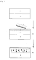
- Fig. 1 is a schematic view showing the process of fabricating an SiC layer in which recombination centers are reduced while utilizing the method according to a preferred embodiment of the present invention.
- an epitaxial layer (E) is grown from the surface of an SiC substrate (S).
- a known method preferably chemical vapor deposition (CVD), is applied to the growth of the epitaxial layer (E).
- step (a) carbon atoms (C) are ion-implanted into a shallow surface layer (A) of the epitaxial layer (E). By the above step, excess carbon interstitials are introduced into the surface layer (A).
- step (b) by heating the SiC crystal layer, carbon interstitials introduced into the surface layer (A) are diffused out from the surface layer (A) to the epitaxial layer (E) that is a bulk layer under the surface layer (A). At this time, during the step (b), carbon interstitials vanish together with carbon vacancies in the epitaxial layer (E), or other defects that are not electrically active are formed. As a result, the electrically active point defects that exist in the epitaxial layer (E) are annealed out or made inactive.
- the step (a) for implanting carbon atoms (C) and the step (b) for annealing the SiC crystal layer can be carried out simultaneously. Moreover, the surface layer (A) into which carbon atoms (C) have been implanted can be etched or mechanically removed.
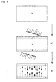
- the quality of the epitaxial layer (E) can be improved. While referring to Fig. 2, the following describes a detailed example in the case where the above steps are applied to a substrate provided with an n-type SiC epitaxial layer in the order of steps.
- an n-type epitaxial layer (E) with a thickness of 50 ⁇ m is grown on an SiC crystal substrate by a known method, preferably by CVD.
- This as-grown epitaxial layer (E) includes vacancies as shown by void circles in the figure.
- a thickness of the epitaxial layer is determined by the withstand voltage of a device to be obtained.
- carbon atoms (C) are implanted into the epitaxial layer (E) to form the surface layer (A) that is a carbon interstitial rich layer with a thickness of 250 nm.
- the concentration of the implanted carbon in the region is almost constant around 1.5E17 cm -3 .
- the epitaxial layer (E) is heated at 1600°C for 30 minutes for annealing to make the carbon implanted therein to diffuse out of the surface layer (A).
- the carbon atoms (interstitials) are attached to and combined with point defects in the epitaxial layer (E) under the surface layer (A) to make the point defects electrically inactive. Since more carbon has been implanted into the surface layer (A) than there are electrically active defects in the epilayer (E), all the defects can be made inactive. In this way, the epitaxial layer (E) under the surface layer (A) will have the reduced concentration of the electrically active point defects.
- the surface layer (A) at the upper edge into which carbon atoms (C) have been implanted contains defects in relation to an implantation damage. Therefore, the surface layer (A) is removed by reactive ion etching (RIE) using CH 4 and O 2 gases in order to demonstrate the influence of the innovation of the implanted carbon atoms (C) to the epitaxial layer (E) under the surface layer (A).
- RIE reactive ion etching
- a thickness to be removed by RIE is in the range of 400 nm from the surface.
- the surface layer (A) can be left or removed by other known techniques depending on the application.
- the surface of the epitaxial layer (E) can be oxidized using high temperature oxygen to form an SiO 2 oxide film with a thickness of approximately 100 nm, and the oxide film can be removed.
- FIG. 3 is a schematic view showing the process of fabricating an SiC layer in which recombination centers are reduced while utilizing the method according to another preferred embodiment of the present invention.
- an SiC bulk crystal (B) is used as an SiC crystal.
- the SiC bulk crystal (B) can also be a wafer sliced from an as-grown SiC bulk crystal.
- Such an SiC bulk crystal (B) is a bulk-like crystal that has been obtained by the sublimation method, the HTCVD method, or the like.
- An SiC wafer can be obtained by slicing such a bulk crystal, for instance, at a thickness in the range from 300 to 400 ⁇ m.
- the electrically active point defects formed during the growth of a crystal or the like are contained therein.
- the carbon atoms (C) are ion-implanted into the shallow surface layer (A) on the upper face side of the SiC bulk crystal (B).
- excess carbon interstitials are introduced into the surface layer (A).
- the carbon atoms (C) implanted into the surface layer (A) are diffused out from the surface layer (A) into the SiC bulk crystal (B) under the surface layer (A).
- carbon interstitials vanish together with carbon vacancies in the SiC bulk crystal (B), or other defects that are not electrically active are formed.
- the electrically active point defects that exist in the SiC bulk crystal (B) are annealed out or made inactive.
- the step (a) for implanting carbon atoms (C) and the step (b) for annealing the SiC bulk crystal (B) can be carried out simultaneously. Moreover, the surface layer (A) into which carbon atoms (C) have been implanted can be etched or mechanically removed.
- Fig. 4 is a schematic view showing the process of fabricating an SiC layer in which recombination centers are reduced while utilizing the method according to another preferred embodiment of the present invention.
- an SiC bulk crystal (B) is used as an SiC crystal.
- this case includes a case in which an optional epitaxial layer exists on the SiC bulk crystal shown in Fig. 4.
- carbon atoms (C) are ion-implanted into the surface layer (A) on the upper face side of the SiC bulk crystal (B), and carbon interstitials are diffused out into the SiC bulk crystal (B) under the surface layer (A) by annealing.
- the carbon atoms (C) are ion-implanted into the shallow surface layer (A) on the lower face side of the SiC bulk crystal (B).
- excess carbon interstitials are introduced into the surface layer (A) on the lower face side.
- the carbon atoms (C) implanted into the surface layer (A) are diffused out from the surface layer (A) into the SiC bulk crystal (B) on the surface layer (A) and into the epitaxial layer thereon.
- carbon interstitials vanish together with carbon vacancies in the SiC bulk crystal (B), or other defects that are not electrically active are formed.
- the electrically active point defects that exist in the SiC bulk crystal (B) and the epitaxial layer are annealed out or made inactive.
- the carbon atoms (C) are ion-implanted into the surface layer (A) on the lower face side of the SiC bulk crystal (B) and are diffused out into the SiC bulk crystal (B) on the surface layer (A) and into the epitaxial layer thereon. Consequently, in particular, the electrically active point defects can be sufficiently eliminated or reduced in a region from around the lower face of the SiC bulk crystal (B) and the epitaxial layer to inside thereof.
- Fig. 5 is a schematic view showing the process of fabricating an SiC layer in which recombination centers are reduced while utilizing the method according to another preferred embodiment of the present invention.
- an SiC bulk crystal (B) is used as an SiC crystal.
- the carbon atoms (C) are ion-implanted into the shallow surface layers (A) on the upper and lower face sides of the SiC bulk crystal (B).
- excess carbon interstitials are introduced into the surface layers (A) on the upper and lower face sides.
- the step (b) by heating the SiC bulk crystal (B), the carbon atoms (C) implanted into the surface layers (A) are diffused out into the SiC bulk crystal (B) inside the surface layers (A). During the annealing, carbon interstitials vanish together with carbon vacancies in the SiC bulk crystal (B), or other defects that are not electrically active are formed. As a result, the electrically active point defects that exist in the SiC bulk crystal (B) are annealed out or made inactive.
- the carbon atoms (C) are ion-implanted into the surface layers (A) on the both face sides of the SiC bulk crystal (B) and are diffused out into the SiC bulk crystal (B) inside the surface layers (A). Consequently, in particular, the electrically active point defects can be sufficiently eliminated or reduced in a region from around the both faces of the SiC bulk crystal (B) to inside thereof.
- Fig. 6 is a schematic view showing the process of fabricating an SiC layer in which recombination centers are reduced while utilizing the method according to another preferred embodiment of the present invention.
- the carbon atoms (C) are ion-implanted into the shallow surface layer (A) of the SiC bulk crystal (B).
- excess carbon interstitials are introduced into the surface layer (A).
- an SiC layer is grown upward from the edge face of the surface layer (A) into which the carbon atoms (C) have been implanted in order to form an epitaxial layer (E).
- the carbon atoms (C) implanted into the surface layer (A) are diffused out from the surface layer (A) into the epitaxial layer (E).
- carbon interstitials vanish together with carbon vacancies in the epitaxial layer (E), or other defects that are not electrically active are formed.
- the carbon atoms (C) implanted into the surface layer (A) are also diffused out from the surface layer (A) into the SiC bulk crystal (B) on the opposite side of the epitaxial layer (E).
- carbon interstitials vanish together with carbon vacancies in the SiC bulk crystal (B), particularly in a region around and inside the surface layer (A), or other defects that are not electrically active are formed.
- the electrically active point defects that exist in the epitaxial layer (E) and the SiC bulk crystal (B) are annealed out or made inactive. Annealing in the above step (b) can be carried out simultaneously with the step of growing the epitaxial layer (E) on the SiC bulk crystal (B) during heating in a CVD chamber.
- Fig. 7 is a schematic view showing the process of fabricating an SiC layer in which recombination centers are reduced while utilizing the method according to another preferred embodiment of the present invention.
- step (a) carbon atoms (C) are ion-implanted into a shallow surface layer (A) of the epitaxial layer (E). By the above step, excess carbon interstitials are introduced into the surface layer (A).
- an SiC epitaxial layer (E1) is grown upward from the edge face of the surface layer (A) into which the carbon atoms (C) have been implanted.
- the carbon atoms (C) implanted into the surface layer (A) are diffused out from the surface layer (A) into the epitaxial layer (E1).
- carbon interstitials vanish together with carbon vacancies in the epitaxial layer (E1), or other defects that are not electrically active are formed.
- the carbon atoms (C) implanted into the surface layer (A) are also diffused out from the surface layer (A) into the epitaxial layer (E) on the opposite side of the epitaxial layer (E1).
- carbon interstitials vanish together with carbon vacancies in the epitaxial layer (E), or other defects that are not electrically active are formed.
- step (c) carbon atoms (C) are then ion-implanted into a shallow surface layer (A) at the outside edge face of the epitaxial layer (E1). By the above step, excess carbon interstitials are introduced into the surface layer (A).
- an SiC epitaxial layer (E2) is grown upward from the edge face of the surface layer (A) into which the carbon atoms (C) have been implanted.
- the carbon atoms (C) implanted into the surface layer (A) are diffused out from the surface layer (A) into the epitaxial layer (E2).
- carbon interstitials vanish together with carbon vacancies in the epitaxial layer (E2), or other defects that are not electrically active are formed.
- the carbon atoms (C) implanted into the surface layer (A) are also diffused out from the surface layer (A) into the epitaxial layer (E1) on the opposite side of the epitaxial layer (E2).
- carbon interstitials vanish together with carbon vacancies in the epitaxial layer (E1), or other defects that are not electrically active are formed.
- the electrically active point defects that exist in the epitaxial layers (E), (E1), and (E2) particularly the electrically active point defects that exist around the interface of the epitaxial layers (E) and (E1) and around the interface of the epitaxial layers (E1) and (E2) are annealed out or made inactive.
- Annealing in the above steps (b) and (d) can be carried out simultaneously with the step of growing the epitaxial layer (E1) or the epitaxial layer (E2) during heating in a CVD chamber.
- a new epitaxial layer can also be formed on the epitaxial layer (E2) by repeating the above described operation.
- epitaxial layers of n layers are further formed on the epitaxial layer (E). Consequently, there is obtained the epitaxial layers composed of a plurality of layers with less electrically active point defects.
- Fig. 16 illustrates the DLTS spectra of two SiC crystal samples, where the sample (1) was prepared according to the preferred embodiment of the present invention, and the sample (2) was prepared under the identical conditions as the sample (1) but omitting the step (a).
- Fig. 17 illustrates the results of the measurement of the minority carrier lifetime by photoluminescence decay, where the sample (1) was prepared according to the preferred embodiment of the present invention, and the sample (2) was prepared under the identical conditions as the sample (1) but omitting the step (a).
- Fig. 18 illustrates the results of the measurement of the minority carrier lifetime at different annealing temperatures by photoluminescence decay, where the sample (1) was prepared according to the preferred embodiment of the present invention, and the sample (2) was prepared under the identical conditions as the sample (1) but omitting the step (a).
- the annealing time was 30 minutes respectively.
- the annealing temperature can be lowered to approximately 1200°C by further lengthening the annealing time.
- the upper limit of the annealing temperature is approximately 2200°C that is equivalent to the sublimation temperature of SiC.
- the method of improving the quality of an SiC crystal described in each of the above embodiments is applied to the production of SiC semiconductor devices of many kinds.
- the method is preferably applied to the production of bipolar type SiC semiconductor devices in which a reduction of electrically active point defects is particularly effective.
- a preferred embodiment of such a bipolar type SiC semiconductor device is described below.
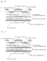
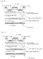
- Fig. 8 is a schematic view showing the cross section of the device structure of an SiC pn diode according to a preferred embodiment of the present invention.
- the SiC pn diode 10 is provided with a high-doped p-type layer, a low-doped n-type base layer, and a high-doped n-type layer.
- the SiC crystal type, the suitable range of a detailed thickness and an impurity concentration of each layer, and the combination thereof in the device structure are well known to one of ordinary skill in the art.
- a low-doped n-type SiC base layer 12 is formed on a high-doped n-type SiC layer 11 by the epitaxial growth method, and a high-doped p-type SiC layer 13 is formed thereon by the epitaxial growth method.
- An anode 15 is formed on the surface of the high-doped p-type SiC layer 13, and a cathode 16 is formed on the surface of the high-doped n-type SiC layer 11.
- Numeral 14 represents a p-type ion implanted layer for relaxing an electric field concentration to improve a withstand voltage characteristics.
- a carbon diffused region 200 by diffusing out carbon interstitials in a carbon implanted layer 100, which has been formed by ion-implanting carbon atoms (C) into a region around the surface of the high-doped p-type SiC layer 13 or into the high-doped n-type SiC layer 11, into the low-doped n-type SiC base layer 12 by annealing.
- C carbon atoms
- the carbon diffused region 200 is formed in a conductivity modulation layer in which electrically active defects influence device characteristics, and electrically active point defects are reduced by combining the carbon interstitials and point defects. Consequently, the SiC pn diode 10 has excellent device characteristics.
- Fig. 9 is a schematic view showing the cross section of the device structure of an SiC pn diode according to another preferred embodiment of the present invention.
- a low-doped p-type SiC base layer 22 is formed on a high-doped p-type SiC layer 21 by the epitaxial growth method, and a high-doped n-type SiC layer 23 is formed thereon by the epitaxial growth method.
- a cathode 25 is formed on the surface of the high-doped n-type SiC layer 23, and an anode 26 is formed on the surface of the high-doped p-type SiC layer 21.
- Numeral 24 represents an n-type ion implanted layer for relaxing an electric field concentration to improve a withstand voltage characteristics.
- a carbon diffused region 200 by diffusing out carbon interstitials in a carbon implanted layer 100, which has been formed by ion-implanting carbon atoms (C) into a region around the surface of the high-doped n-type SiC layer 23 or into the high-doped p-type SiC layer 21, into the low-doped p-type SiC base layer 22 by annealing.
- C carbon atoms
- the carbon diffused region 200 is formed in a conductivity modulation layer in which electrically active defects influence device characteristics, and electrically active point defects are reduced by combining the carbon interstitials and point defects. Consequently, the SiC pn diode 20 has excellent device characteristics.
- Fig. 10 is a schematic view showing the cross section of the device structure of an SiC npn transistor according to a preferred embodiment of the present invention.
- the SiC npn transistor 30 is provided with an n-type emitter layer, a p-type base layer, and an n-type collector layer.
- the SiC crystal type, the suitable range of a detailed thickness and an impurity concentration of each layer, and the combination thereof in the device structure are well known to one of ordinary skill in the art.
- a p-type SiC base layer 31 is formed on an n-type SiC collector layer 32 by the epitaxial growth method, and an n-type SiC emitter layer 33 is formed thereon by the epitaxial growth method.
- a high-doped p-type ion implanted layer 34 is formed around the surface of the p-type SiC base layer 31 and on the periphery of the n-type SiC emitter layer 33, and a gate electrode 35 is formed thereon.
- An emitter electrode 36 is formed on the surface of the n-type SiC emitter layer 33, and a collector electrode 37 is formed on the surface of the n-type SiC collector layer 32.
- a carbon diffused region 200 by diffusing out carbon interstitials in a carbon implanted layer 100, which has been formed by ion-implanting carbon atoms (C) into a region around the surface of the n-type SiC emitter layer 33 or into the n-type SiC collector layer 32, into the p-type SiC base layer 31 by annealing.
- C carbon atoms
- the carbon diffused region 200 is formed in a conductivity modulation layer in which electrically active defects influence device characteristics, and electrically active point defects are reduced by combining the carbon interstitials and point defects. Consequently, the SiC npn transistor 30 has excellent device characteristics.
- Fig. 11 is a schematic view showing the cross section of the device structure of an SiC pnp transistor according to a preferred embodiment of the present invention.
- the SiC pnp transistor 40 an n-type SiC base layer 41 is formed on a p-type SiC collector layer 42 by the epitaxial growth method, and a p-type SiC emitter layer 43 is formed thereon by the epitaxial growth method.
- a high-doped n-type ion implanted layer 44 is formed around the surface of the n-type SiC base layer 41 and on the periphery of the p-type SiC emitter layer 43, and a gate electrode 45 is formed thereon.
- An emitter electrode 46 is formed on the surface of the p-type SiC emitter layer 43, and a collector electrode 47 is formed on the surface of the p-type SiC collector layer 42.
- a carbon diffused region 200 by diffusing out carbon interstitials in a carbon implanted layer 100, which has been formed by ion-implanting carbon atoms (C) into a region around the surface of the p-type SiC emitter layer 43 or into the p-type SiC collector layer 42, into the n-type SiC base layer 41 by annealing.
- C carbon atoms
- the carbon diffused region 200 is formed in a conductivity modulation layer in which electrically active defects influence device characteristics, and electrically active point defects are reduced by combining the carbon interstitials and point defects. Consequently, the SiC pnp transistor 40 has excellent device characteristics.
- Fig. 12 is a schematic view showing the cross section of the device structure of an SiC thyristor according to a preferred embodiment of the present invention.
- the SiC thyristor 50 is an SiC gate turn-off thyristor that is provided with a p-type layer, an n-type base layer, a p-type base layer, and an n-type layer.
- the SiC crystal type, the suitable range of a detailed thickness and an impurity concentration of each layer, and the combination thereof in the device structure are well known to one of ordinary skill in the art.
- a p-type SiC base layer 52 is formed on an n-type SiC layer 51 by the epitaxial growth method, an n-type SiC base layer 53 is formed thereon by the epitaxial growth method, and a p-type SiC layer 54 is formed thereon by the epitaxial growth method.
- a high-doped n-type ion implanted layer 55 is formed around the surface of the n-type SiC base layer 53 and on the periphery of the p-type SiC layer 54, and a gate electrode 56 is formed thereon.
- An anode 57 is formed on the surface of the p-type SiC layer 54, and a cathode 58 is formed on the surface of the n-type SiC layer 51.
- a carbon diffused region 200 by diffusing out carbon interstitials in a carbon implanted layer 100, which has been formed by ion-implanting carbon atoms (C) into a region around the surface of the p-type SiC layer 54 or into the n-type SiC layer 51, into the p-type SiC base layer 52 and the n-type SiC base layer 53 by annealing.
- C carbon atoms
- the carbon diffused region 200 is formed in a conductivity modulation layer in which electrically active defects influence device characteristics, and electrically active point defects are reduced by combining the carbon interstitials and point defects. Consequently, the SiC thyristor 50 has excellent device characteristics.
- Fig. 13 is a schematic view showing the cross section of the device structure of an SiC thyristor according to a preferred embodiment of the present invention.
- an n-type SiC base layer 62 is formed on a p-type SiC layer 61 by the epitaxial growth method, a p-type SiC base layer 63 is formed thereon by the epitaxial growth method, and an n-type SiC layer 64 is formed thereon by the epitaxial growth method.
- a high-doped p-type ion implanted layer 65 is formed around the surface of the p-type SiC base layer 63 and on the periphery of the n-type SiC layer 64, and a gate electrode 66 is formed thereon.
- a cathode 67 is formed on the surface of the n-type SiC layer 64, and an anode 68 is formed on the surface of the p-type SiC layer 61.
- a carbon diffused region 200 by diffusing out carbon interstitials in a carbon implanted layer 100, which has been formed by ion-implanting carbon atoms (C) into a region around the surface of the n-type SiC layer 64 or into the p-type SiC layer 61, into the n-type SiC base layer 62 and the p-type SiC base layer 63 by annealing.
- C carbon atoms
- the carbon diffused region 200 is formed in a conductivity modulation layer in which electrically active defects influence device characteristics, and electrically active point defects are reduced by combining the carbon interstitials and point defects. Consequently, the SiC thyristor 60 has excellent device characteristics.
- Fig. 14 is a schematic view showing the cross section of the device structure of an SiC IGBT according to a preferred embodiment of the present invention.
- the SiC IGBT 70 is provided with a p-type layer, an n-type base layer, a p-type base layer, and an n-type collector layer.
- the SiC crystal type, the suitable range of a detailed thickness and an impurity concentration of each layer, and the combination thereof in the device structure are well known to one of ordinary skill in the art.
- a p-type SiC base layer 71 is formed on an n-type SiC collector layer 72 by the epitaxial growth method.
- a gate electrode 75 is formed on the p-type SiC base layer 71 through an oxide film 78 as a gate insulating film.
- an n-type base layer 74 is formed above the p-type SiC base layer 71, and an emitter electrode 76 is formed thereon.
- the n-type base layer 74 is formed in the range from the oxide film 78 under the gate electrode 75 to the emitter electrode 76, and a p-type layer 73 is formed in the range from the oxide film 78 to the emitter electrode 76 inside the n-type base layer 74.
- a collector electrode 77 is formed on the surface of the n-type SiC collector layer 72.
- the p-type SiC base layer 71 by applying any of the methods shown in Figs. 1 to 7, there is formed a carbon diffused region 200 by diffusing out carbon interstitials in a carbon implanted layer 100, which has been formed by ion-implanting carbon atoms (C) into a region around the surface of the p-type SiC base layer 71 on the n-type base layer 74 side or into the n-type SiC collector layer 72, into the p-type SiC base layer 71 by annealing.
- C carbon atoms
- the carbon diffused region 200 is formed in a conductivity modulation layer in which electrically active defects influence device characteristics, and electrically active point defects are reduced by combining the carbon interstitials and point defects. Consequently, the SiC IGBT 70 has excellent device characteristics.
- Fig. 15 is a schematic view showing the cross section of the device structure of an SiC IGBT according to a preferred embodiment of the present invention.
- an n-type SiC base layer 81 is formed on a p-type SiC collector layer 82 by the epitaxial growth method.
- a gate electrode 85 is formed on the n-type SiC base layer 81 through an oxide film 88 as a gate insulating film.
- a p-type base layer 84 is formed above the n-type SiC base layer 81, and an emitter electrode 86 is formed thereon.
- the p-type base layer 84 is formed in the range from the oxide film 88 under the gate electrode 85 to the emitter electrode 86, and an n-type layer 83 is formed in the range from the oxide film 88 to the emitter electrode 86 inside the p-type base layer 84.
- a collector electrode 87 is formed on the surface of the p-type SiC collector layer 82.
- the n-type SiC base layer 81 by applying any of the methods shown in Figs. 1 to 7, there is formed a carbon diffused region 200 by diffusing out carbon interstitials in a carbon implanted layer 100, which has been formed by ion-implanting carbon atoms (C) into a region around the surface of the n-type SiC base layer 81 on the p-type base layer 84 side or into the p-type SiC collector layer 82, into the n-type SiC base layer 81 by annealing.
- C carbon atoms
- the carbon diffused region 200 is formed in a conductivity modulation layer in which electrically active defects influence device characteristics, and electrically active point defects are reduced by combining the carbon interstitials and point defects. Consequently, the SiC IGBT 80 has excellent device characteristics.
- crystal as used herein means an excellent periodicity of the lattice in the three dimensions over greater regions, i.e. typical polycrystalline structures are excluded.
Landscapes
- Chemical & Material Sciences (AREA)
- Crystallography & Structural Chemistry (AREA)
- Organic Chemistry (AREA)
- Engineering & Computer Science (AREA)
- Materials Engineering (AREA)
- Metallurgy (AREA)
- Inorganic Chemistry (AREA)
- Physics & Mathematics (AREA)
- Electromagnetism (AREA)
- Recrystallisation Techniques (AREA)
- Bipolar Transistors (AREA)
- Thyristors (AREA)
- Formation Of Insulating Films (AREA)
- Crystals, And After-Treatments Of Crystals (AREA)
Applications Claiming Priority (2)
| Application Number | Priority Date | Filing Date | Title |
|---|---|---|---|
| JP2006206953 | 2006-07-28 | ||
| JP2006237996A JP5155536B2 (ja) | 2006-07-28 | 2006-09-01 | SiC結晶の質を向上させる方法およびSiC半導体素子の製造方法 |
Publications (3)
| Publication Number | Publication Date |
|---|---|
| EP1883102A2 true EP1883102A2 (de) | 2008-01-30 |
| EP1883102A3 EP1883102A3 (de) | 2009-04-22 |
| EP1883102B1 EP1883102B1 (de) | 2013-10-02 |
Family
ID=38596418
Family Applications (1)
| Application Number | Title | Priority Date | Filing Date |
|---|---|---|---|
| EP06255833.3A Active EP1883102B1 (de) | 2006-07-28 | 2006-11-15 | Verfahren zur Verbesserung der Qualität eines SiC-Kristalls und ein SiC-Halbleiterbauelement. |
Country Status (6)
| Country | Link |
|---|---|
| US (4) | US7737011B2 (de) |
| EP (1) | EP1883102B1 (de) |
| JP (1) | JP5155536B2 (de) |
| KR (1) | KR101287017B1 (de) |
| CN (1) | CN101114593B (de) |
| TW (1) | TWI384555B (de) |
Cited By (4)
| Publication number | Priority date | Publication date | Assignee | Title |
|---|---|---|---|---|
| EP2922094A3 (de) * | 2014-03-20 | 2015-12-02 | Kabushiki Kaisha Toshiba | Halbleiterbauelement und Herstellungsverfahren dafür |
| EP3026694A1 (de) * | 2014-11-26 | 2016-06-01 | Kabushiki Kaisha Toshiba | Sic halbleiterbauelement und seine herstellungsverfahren |
| US9508802B2 (en) | 2011-05-16 | 2016-11-29 | Toyota Jidosha Kabushiki Kaisha | Gettering process for producing semiconductor device |
| CN108431925A (zh) * | 2015-12-22 | 2018-08-21 | 瓦里安半导体设备公司 | 对衬底的掺杂剂扩散的无损强化 |
Families Citing this family (64)
| Publication number | Priority date | Publication date | Assignee | Title |
|---|---|---|---|---|
| US7895548B2 (en) * | 2007-10-26 | 2011-02-22 | Synopsys, Inc. | Filler cells for design optimization in a place-and-route system |
| US20090108408A1 (en) * | 2007-10-29 | 2009-04-30 | Synopsys, Inc. | Method for Trapping Implant Damage in a Semiconductor Substrate |
| US9472423B2 (en) * | 2007-10-30 | 2016-10-18 | Synopsys, Inc. | Method for suppressing lattice defects in a semiconductor substrate |
| US20110012132A1 (en) * | 2008-02-06 | 2011-01-20 | Rohm Co., Ltd. | Semiconductor Device |
| JP2012012227A (ja) * | 2010-06-29 | 2012-01-19 | New Japan Radio Co Ltd | 結晶欠陥の除去方法 |
| JP5870478B2 (ja) * | 2010-09-30 | 2016-03-01 | 富士通セミコンダクター株式会社 | 半導体装置の製造方法 |
| JP6042658B2 (ja) * | 2011-09-07 | 2016-12-14 | トヨタ自動車株式会社 | SiC半導体素子の製造方法 |
| JP5802492B2 (ja) | 2011-09-09 | 2015-10-28 | 株式会社東芝 | 半導体素子及びその製造方法 |
| JP5759393B2 (ja) | 2012-01-12 | 2015-08-05 | 住友電気工業株式会社 | 炭化珪素半導体装置の製造方法 |
| JP5615303B2 (ja) * | 2012-01-24 | 2014-10-29 | 三菱電機株式会社 | 不純物濃度測定方法および不純物濃度測定装置 |
| JP6032831B2 (ja) * | 2012-03-07 | 2016-11-30 | 国立研究開発法人産業技術総合研究所 | SiC半導体装置及びその製造方法 |
| US9590047B2 (en) * | 2012-04-04 | 2017-03-07 | Fairchild Semiconductor Corporation | SiC bipolar junction transistor with reduced carrier lifetime in collector and a defect termination layer |
| US10541306B2 (en) * | 2012-09-12 | 2020-01-21 | Cree, Inc. | Using a carbon vacancy reduction material to increase average carrier lifetime in a silicon carbide semiconductor device |
| JP2014146748A (ja) * | 2013-01-30 | 2014-08-14 | Toshiba Corp | 半導体装置及びその製造方法並びに半導体基板 |
| US9526215B2 (en) * | 2013-03-05 | 2016-12-27 | Xiant Technologies, Inc. | Photon modulation management system |
| JP6376729B2 (ja) * | 2013-05-21 | 2018-08-22 | ローム株式会社 | 半導体装置の製造方法 |
| JP6178181B2 (ja) | 2013-09-12 | 2017-08-09 | 株式会社東芝 | 半導体装置及びその製造方法 |
| WO2015072210A1 (ja) * | 2013-11-13 | 2015-05-21 | 三菱電機株式会社 | 半導体装置の製造方法 |
| CN105830220B (zh) * | 2013-12-13 | 2019-05-28 | 三菱电机株式会社 | 半导体装置的制造方法 |
| CN105900221B (zh) * | 2014-02-28 | 2019-01-22 | 三菱电机株式会社 | 半导体装置以及半导体装置的制造方法 |
| JP2015176995A (ja) | 2014-03-14 | 2015-10-05 | 株式会社東芝 | 半導体装置およびその製造方法 |
| JP6289952B2 (ja) * | 2014-03-19 | 2018-03-07 | 株式会社東芝 | SiCエピタキシャル基板の製造方法、半導体装置の製造方法 |
| JP6271309B2 (ja) | 2014-03-19 | 2018-01-31 | 株式会社東芝 | 半導体基板の製造方法、半導体基板および半導体装置 |
| JP6271356B2 (ja) * | 2014-07-07 | 2018-01-31 | 株式会社東芝 | 半導体装置の製造方法 |
| JP6539959B2 (ja) * | 2014-08-28 | 2019-07-10 | 株式会社Sumco | エピタキシャルシリコンウェーハおよびその製造方法、ならびに、固体撮像素子の製造方法 |
| JP6208106B2 (ja) * | 2014-09-19 | 2017-10-04 | 株式会社東芝 | 半導体装置及びその製造方法 |
| JP2016063190A (ja) | 2014-09-22 | 2016-04-25 | 住友電気工業株式会社 | 炭化珪素エピタキシャル基板の製造方法、炭化珪素エピタキシャル基板および炭化珪素半導体装置 |
| DE102014116666B4 (de) | 2014-11-14 | 2022-04-21 | Infineon Technologies Ag | Ein Verfahren zum Bilden eines Halbleiterbauelements |
| JP2016100455A (ja) * | 2014-11-21 | 2016-05-30 | 三菱電機株式会社 | 半導体装置及びその製造方法 |
| CN105762116B (zh) * | 2014-12-16 | 2018-09-18 | 中芯国际集成电路制造(上海)有限公司 | 硅衬底、其制作方法及包括其的ipd器件 |
| JP2016127177A (ja) * | 2015-01-06 | 2016-07-11 | 住友電気工業株式会社 | 炭化珪素基板、炭化珪素半導体装置および炭化珪素基板の製造方法 |
| EP3279927A4 (de) * | 2015-03-31 | 2018-11-14 | Hamamatsu Photonics K.K. | Halbleiterbauelement |
| DE102015111213B4 (de) * | 2015-07-10 | 2023-05-04 | Infineon Technologies Ag | Verfahren zum Verringern einer bipolaren Degradation bei einem SiC-Halbleiterbauelement und Halbleiterbauelement |
| JP6584253B2 (ja) * | 2015-09-16 | 2019-10-02 | ローム株式会社 | SiCエピタキシャルウェハ、SiCエピタキシャルウェハの製造装置、SiCエピタキシャルウェハの製造方法、および半導体装置 |
| CN105551794B (zh) * | 2015-12-29 | 2017-10-10 | 中国科学院上海硅酸盐研究所 | 一种SiC基稀磁半导体薄膜及其制备方法 |
| FR3048548B1 (fr) * | 2016-03-02 | 2018-03-02 | Soitec | Procede de determination d'une energie convenable d'implantation dans un substrat donneur et procede de fabrication d'une structure de type semi-conducteur sur isolant |
| US11058889B1 (en) | 2017-04-03 | 2021-07-13 | Xiant Technologies, Inc. | Method of using photon modulation for regulation of hormones in mammals |
| JP6567601B2 (ja) * | 2017-06-19 | 2019-08-28 | 株式会社東芝 | 半導体装置 |
| CN109273405B (zh) * | 2017-07-18 | 2021-06-08 | 上海新昇半导体科技有限公司 | 一种半导体器件及其制造方法、电子装置 |
| CN107492482B (zh) * | 2017-07-18 | 2019-11-22 | 李哲洋 | 一种提高碳化硅外延层载流子寿命的方法 |
| CN109037338B (zh) * | 2018-07-12 | 2021-04-30 | 中国电子科技集团公司第五十八研究所 | 一种mosfet功率器件的制备方法 |
| US11127817B2 (en) * | 2018-07-13 | 2021-09-21 | Taiwan Semiconductor Manufacturing Co., Ltd. | Formation of semiconductor device structure by implantation |
| US11121235B2 (en) | 2018-07-25 | 2021-09-14 | National Tsing Hua University | Structure and a manufacturing method of a MOSFET with an element of IVA group ion implantation |
| KR102375530B1 (ko) * | 2018-10-16 | 2022-03-16 | 에스아이씨씨 컴퍼니 리미티드 | 소량의 바나듐이 도핑된 반절연 탄화규소 단결정, 기판, 제조 방법 |
| CN110106550A (zh) * | 2019-05-15 | 2019-08-09 | 中国电子科技集团公司第十三研究所 | 一种外延片的制备方法 |
| CN110164959A (zh) * | 2019-05-15 | 2019-08-23 | 中国电子科技集团公司第十三研究所 | 一种衬底及外延片 |
| DE102019118803A1 (de) | 2019-07-11 | 2021-01-14 | Infineon Technologies Ag | Verfahren zum herstellen einer halbleitervorrichtung und halbleitervorrichtung |
| CN111243941A (zh) * | 2020-01-15 | 2020-06-05 | 中国科学院半导体研究所 | 提高碳化硅少子寿命的方法 |
| TWI865578B (zh) * | 2020-06-18 | 2024-12-11 | 盛新材料科技股份有限公司 | 半絕緣單晶碳化矽塊材以及粉末 |
| CN111900097B (zh) * | 2020-06-28 | 2022-11-25 | 北京大学 | 检测宽禁带半导体中深能级缺陷态的方法 |
| CN111865250B (zh) * | 2020-07-10 | 2021-10-19 | 中国科学院上海微系统与信息技术研究所 | 一种poi衬底、高频声波谐振器及其制备方法 |
| JP6903254B1 (ja) * | 2020-12-15 | 2021-07-14 | 三菱電機株式会社 | 半導体装置の製造方法、及び、半導体装置 |
| JP6903362B1 (ja) | 2021-02-05 | 2021-07-14 | 株式会社Brillar | 合成宝石用結晶体の製造方法 |
| CN113013260B (zh) * | 2021-02-23 | 2022-08-23 | 温州大学 | 一种光敏型SiC异构结多势垒变容二极管 |
| CN113024277B (zh) * | 2021-03-03 | 2022-01-28 | 西南科技大学 | 高密度层错的碳化硅材料及其制备方法 |
| EP4095888B1 (de) | 2021-05-28 | 2024-12-18 | Hitachi Energy Ltd | Halbleiterbauelement mit einer reduzierten konzentration an kohlenstoffvakanzen und verfahren zur herstellung eines halbleiterbauelements |
| CN114999900B (zh) * | 2022-07-18 | 2023-08-08 | 浙江大学杭州国际科创中心 | 一种提高碳化硅晶圆中少数载流子寿命的方法 |
| CN115050637B (zh) * | 2022-07-18 | 2025-09-02 | 浙江大学杭州国际科创中心 | 一种提高碳化硅晶圆表面寿命的方法 |
| JP2026502724A (ja) * | 2023-02-13 | 2026-01-23 | ヒタチ・エナジー・リミテッド | 半導体装置の製造方法および半導体装置 |
| CN116387141B (zh) * | 2023-06-07 | 2023-10-13 | 浙江大学杭州国际科创中心 | 一种低裂纹碳化硅晶圆制备方法及碳化硅晶圆 |
| CN121753529A (zh) * | 2023-08-28 | 2026-03-27 | 日立能源有限公司 | 用于半导体器件的半绝缘SiC衬底 |
| CN118338770B (zh) * | 2024-06-12 | 2024-09-03 | 浙江大学杭州国际科创中心 | 碳化硅光电神经突触器件及其制备方法与应用 |
| EP4679491A1 (de) * | 2024-07-08 | 2026-01-14 | Hitachi Energy Ltd | Verfahren zur herstellung eines wachstumssubstrats, verfahren zur herstellung einer epitaktischen siliciumcarbidschicht, wachstumssubstrat und epitaktische siliciumcarbidschicht |
| CN118983215A (zh) * | 2024-10-22 | 2024-11-19 | 河北普兴电子科技股份有限公司 | 一种提升少子寿命的碳化硅外延生长方法及碳化硅外延片 |
Family Cites Families (26)
| Publication number | Priority date | Publication date | Assignee | Title |
|---|---|---|---|---|
| US3710203A (en) | 1971-11-05 | 1973-01-09 | Fmc Corp | High power storage diode |
| IL79107A (en) | 1985-06-17 | 1989-03-31 | De Beers Ind Diamond | Ion implantation in crystalline substrate |
| US5328855A (en) | 1991-07-25 | 1994-07-12 | Matsushita Electric Industrial Co., Ltd. | Formation of semiconductor diamond |
| US5543637A (en) * | 1994-11-14 | 1996-08-06 | North Carolina State University | Silicon carbide semiconductor devices having buried silicon carbide conduction barrier layers therein |
| EP0717435A1 (de) * | 1994-12-01 | 1996-06-19 | AT&T Corp. | Verfahren zur Kontrolle der Diffusion eines Dotiermaterials in einer Halbleiterschicht und dadurch hergestellte Halbleiterschicht |
| JPH09106958A (ja) * | 1995-06-23 | 1997-04-22 | De Beers Ind Diamond Div Ltd | 結晶基体のドーピング |
| JP3647515B2 (ja) * | 1995-08-28 | 2005-05-11 | 株式会社デンソー | p型炭化珪素半導体の製造方法 |
| EP0845803A4 (de) | 1996-04-18 | 2002-03-27 | Matsushita Electric Industrial Co Ltd | SiC-BAUELEMENT UND VERFAHREN ZU SEINER HERSTELLUNG |
| US6273950B1 (en) | 1996-04-18 | 2001-08-14 | Matsushita Electric Industrial Co., Ltd. | SiC device and method for manufacturing the same |
| SE9603608D0 (sv) | 1996-10-03 | 1996-10-03 | Abb Research Ltd | A method for producing a region doped with boron in a SiC-layer |
| JP3060973B2 (ja) * | 1996-12-24 | 2000-07-10 | 日本電気株式会社 | 選択成長法を用いた窒化ガリウム系半導体レーザの製造方法及び窒化ガリウム系半導体レーザ |
| JP3036495B2 (ja) * | 1997-11-07 | 2000-04-24 | 豊田合成株式会社 | 窒化ガリウム系化合物半導体の製造方法 |
| US6265289B1 (en) * | 1998-06-10 | 2001-07-24 | North Carolina State University | Methods of fabricating gallium nitride semiconductor layers by lateral growth from sidewalls into trenches, and gallium nitride semiconductor structures fabricated thereby |
| JP2000068225A (ja) * | 1998-08-26 | 2000-03-03 | Japan Atom Energy Res Inst | 炭化珪素半導体へのイオン注入方法 |
| JP3201475B2 (ja) * | 1998-09-14 | 2001-08-20 | 松下電器産業株式会社 | 半導体装置およびその製造方法 |
| US6177688B1 (en) * | 1998-11-24 | 2001-01-23 | North Carolina State University | Pendeoepitaxial gallium nitride semiconductor layers on silcon carbide substrates |
| JP3770014B2 (ja) * | 1999-02-09 | 2006-04-26 | 日亜化学工業株式会社 | 窒化物半導体素子 |
| AU4941900A (en) * | 1999-05-31 | 2000-12-18 | De Beers Industrial Diamond Division (Proprietary) Limited | Doping of crystalline substrates |
| US6580098B1 (en) * | 1999-07-27 | 2003-06-17 | Toyoda Gosei Co., Ltd. | Method for manufacturing gallium nitride compound semiconductor |
| US6812053B1 (en) * | 1999-10-14 | 2004-11-02 | Cree, Inc. | Single step pendeo- and lateral epitaxial overgrowth of Group III-nitride epitaxial layers with Group III-nitride buffer layer and resulting structures |
| US6521514B1 (en) * | 1999-11-17 | 2003-02-18 | North Carolina State University | Pendeoepitaxial methods of fabricating gallium nitride semiconductor layers on sapphire substrates |
| JP3551909B2 (ja) * | 1999-11-18 | 2004-08-11 | 株式会社デンソー | 炭化珪素半導体装置の製造方法 |
| KR100421038B1 (ko) * | 2001-03-28 | 2004-03-03 | 삼성전자주식회사 | 표면으로부터 오염물을 제거하는 세정 장비 및 이를이용한 세정 방법 |
| ITTO20011129A1 (it) * | 2001-12-04 | 2003-06-04 | Infm Istituto Naz Per La Fisi | Metodo per la soppressione della diffusione anomala transiente di droganti in silicio. |
| US20040144301A1 (en) * | 2003-01-24 | 2004-07-29 | Neudeck Philip G. | Method for growth of bulk crystals by vapor phase epitaxy |
| US6974720B2 (en) | 2003-10-16 | 2005-12-13 | Cree, Inc. | Methods of forming power semiconductor devices using boule-grown silicon carbide drift layers and power semiconductor devices formed thereby |
-
2006
- 2006-09-01 JP JP2006237996A patent/JP5155536B2/ja active Active
- 2006-11-10 US US11/595,232 patent/US7737011B2/en active Active
- 2006-11-15 KR KR1020060113058A patent/KR101287017B1/ko active Active
- 2006-11-15 TW TW095142187A patent/TWI384555B/zh active
- 2006-11-15 EP EP06255833.3A patent/EP1883102B1/de active Active
-
2007
- 2007-01-19 CN CN2007100007551A patent/CN101114593B/zh active Active
-
2008
- 2008-10-14 US US12/250,558 patent/US7834362B2/en active Active
- 2008-10-15 US US12/251,590 patent/US7754589B2/en active Active
-
2010
- 2010-03-16 US US12/724,447 patent/US8815708B2/en active Active
Cited By (8)
| Publication number | Priority date | Publication date | Assignee | Title |
|---|---|---|---|---|
| US9508802B2 (en) | 2011-05-16 | 2016-11-29 | Toyota Jidosha Kabushiki Kaisha | Gettering process for producing semiconductor device |
| EP2710629B1 (de) * | 2011-05-16 | 2020-12-16 | Denso Corporation | Herstellungsverfahren für ein halbleiterbauelement |
| EP2922094A3 (de) * | 2014-03-20 | 2015-12-02 | Kabushiki Kaisha Toshiba | Halbleiterbauelement und Herstellungsverfahren dafür |
| US9786740B2 (en) | 2014-03-20 | 2017-10-10 | Kabushiki Kaisha Toshiba | Semiconductor device and method for producing the same |
| EP3026694A1 (de) * | 2014-11-26 | 2016-06-01 | Kabushiki Kaisha Toshiba | Sic halbleiterbauelement und seine herstellungsverfahren |
| US9716186B2 (en) | 2014-11-26 | 2017-07-25 | Kabushiki Kaisha Toshiba | Semiconductor device manufacturing method, and semiconductor device |
| CN108431925A (zh) * | 2015-12-22 | 2018-08-21 | 瓦里安半导体设备公司 | 对衬底的掺杂剂扩散的无损强化 |
| CN108431925B (zh) * | 2015-12-22 | 2022-08-02 | 瓦里安半导体设备公司 | 对衬底与半导体装置掺杂的方法及对衬底掺杂的系统 |
Also Published As
| Publication number | Publication date |
|---|---|
| EP1883102B1 (de) | 2013-10-02 |
| KR20080011021A (ko) | 2008-01-31 |
| KR101287017B1 (ko) | 2013-07-17 |
| EP1883102A3 (de) | 2009-04-22 |
| US7737011B2 (en) | 2010-06-15 |
| US8815708B2 (en) | 2014-08-26 |
| TW200807559A (en) | 2008-02-01 |
| CN101114593B (zh) | 2011-04-13 |
| US20090047772A1 (en) | 2009-02-19 |
| JP2008053667A (ja) | 2008-03-06 |
| US20100173475A1 (en) | 2010-07-08 |
| US20080026544A1 (en) | 2008-01-31 |
| US20090039358A1 (en) | 2009-02-12 |
| JP5155536B2 (ja) | 2013-03-06 |
| TWI384555B (zh) | 2013-02-01 |
| US7834362B2 (en) | 2010-11-16 |
| CN101114593A (zh) | 2008-01-30 |
| US7754589B2 (en) | 2010-07-13 |
Similar Documents
| Publication | Publication Date | Title |
|---|---|---|
| EP1883102B1 (de) | Verfahren zur Verbesserung der Qualität eines SiC-Kristalls und ein SiC-Halbleiterbauelement. | |
| KR101709364B1 (ko) | 탄화 규소 소자들에 대한 확산된 접합 단자 구조들 및 이를 포함하는 탄화 규소 소자들을 제조하는 방법 | |
| JP6237902B2 (ja) | 半導体装置および半導体装置の製造方法 | |
| US8361893B2 (en) | Semiconductor device and substrate with chalcogen doped region | |
| JP5528515B2 (ja) | SiCバイポーラ型半導体素子 | |
| US8921979B2 (en) | Method for producing a semiconductor layer | |
| CN110582851B (zh) | 半导体装置 | |
| US6703294B1 (en) | Method for producing a region doped with boron in a SiC-layer | |
| JP6976493B1 (ja) | 半導体装置およびその製造方法 | |
| EP4095888B1 (de) | Halbleiterbauelement mit einer reduzierten konzentration an kohlenstoffvakanzen und verfahren zur herstellung eines halbleiterbauelements | |
| JPH09232326A (ja) | 半導体装置の製造方法 | |
| EP4531075A1 (de) | Verfahren zur herstellung von verbesserten sic-substraten und sic-epischichten | |
| US20260011557A1 (en) | Method for producing a semiconductor body, semiconductor body and power semiconductor device | |
| JP4370678B2 (ja) | 炭化けい素半導体素子の製造方法 | |
| KR102563890B1 (ko) | SiC 반도체의 깊은 준위 결함 제거 방법 |
Legal Events
| Date | Code | Title | Description |
|---|---|---|---|
| PUAI | Public reference made under article 153(3) epc to a published international application that has entered the european phase |
Free format text: ORIGINAL CODE: 0009012 |
|
| AK | Designated contracting states |
Kind code of ref document: A2 Designated state(s): AT BE BG CH CY CZ DE DK EE ES FI FR GB GR HU IE IS IT LI LT LU LV MC NL PL PT RO SE SI SK TR |
|
| AX | Request for extension of the european patent |
Extension state: AL BA HR MK YU |
|
| PUAL | Search report despatched |
Free format text: ORIGINAL CODE: 0009013 |
|
| AK | Designated contracting states |
Kind code of ref document: A3 Designated state(s): AT BE BG CH CY CZ DE DK EE ES FI FR GB GR HU IE IS IT LI LT LU LV MC NL PL PT RO SE SI SK TR |
|
| AX | Request for extension of the european patent |
Extension state: AL BA HR MK RS |
|
| 17P | Request for examination filed |
Effective date: 20091021 |
|
| AKX | Designation fees paid |
Designated state(s): DE GB IT SE |
|
| GRAP | Despatch of communication of intention to grant a patent |
Free format text: ORIGINAL CODE: EPIDOSNIGR1 |
|
| INTG | Intention to grant announced |
Effective date: 20130613 |
|
| GRAS | Grant fee paid |
Free format text: ORIGINAL CODE: EPIDOSNIGR3 |
|
| GRAA | (expected) grant |
Free format text: ORIGINAL CODE: 0009210 |
|
| AK | Designated contracting states |
Kind code of ref document: B1 Designated state(s): DE GB IT SE |
|
| REG | Reference to a national code |
Ref country code: GB Ref legal event code: FG4D |
|
| REG | Reference to a national code |
Ref country code: DE Ref legal event code: R096 Ref document number: 602006038650 Country of ref document: DE Effective date: 20131128 |
|
| PG25 | Lapsed in a contracting state [announced via postgrant information from national office to epo] |
Ref country code: SE Free format text: LAPSE BECAUSE OF FAILURE TO SUBMIT A TRANSLATION OF THE DESCRIPTION OR TO PAY THE FEE WITHIN THE PRESCRIBED TIME-LIMIT Effective date: 20131002 |
|
| REG | Reference to a national code |
Ref country code: DE Ref legal event code: R097 Ref document number: 602006038650 Country of ref document: DE |
|
| PLBE | No opposition filed within time limit |
Free format text: ORIGINAL CODE: 0009261 |
|
| STAA | Information on the status of an ep patent application or granted ep patent |
Free format text: STATUS: NO OPPOSITION FILED WITHIN TIME LIMIT |
|
| PG25 | Lapsed in a contracting state [announced via postgrant information from national office to epo] |
Ref country code: IT Free format text: LAPSE BECAUSE OF FAILURE TO SUBMIT A TRANSLATION OF THE DESCRIPTION OR TO PAY THE FEE WITHIN THE PRESCRIBED TIME-LIMIT Effective date: 20131002 |
|
| 26N | No opposition filed |
Effective date: 20140703 |
|
| GBPC | Gb: european patent ceased through non-payment of renewal fee |
Effective date: 20140102 |
|
| REG | Reference to a national code |
Ref country code: DE Ref legal event code: R097 Ref document number: 602006038650 Country of ref document: DE Effective date: 20140703 |
|
| PG25 | Lapsed in a contracting state [announced via postgrant information from national office to epo] |
Ref country code: GB Free format text: LAPSE BECAUSE OF NON-PAYMENT OF DUE FEES Effective date: 20140102 |
|
| REG | Reference to a national code |
Ref country code: DE Ref legal event code: R082 Ref document number: 602006038650 Country of ref document: DE |
|
| REG | Reference to a national code |
Ref country code: DE Ref legal event code: R079 Ref document number: 602006038650 Country of ref document: DE Free format text: PREVIOUS MAIN CLASS: H01L0021040000 Ipc: H10P0095000000 |
|
| PGFP | Annual fee paid to national office [announced via postgrant information from national office to epo] |
Ref country code: DE Payment date: 20251118 Year of fee payment: 20 |