EP1883138A2 - Lampenfassung, Rückbeleuchtungsanordnung und Anzeigevorrichtung - Google Patents
Lampenfassung, Rückbeleuchtungsanordnung und Anzeigevorrichtung Download PDFInfo
- Publication number
- EP1883138A2 EP1883138A2 EP07014463A EP07014463A EP1883138A2 EP 1883138 A2 EP1883138 A2 EP 1883138A2 EP 07014463 A EP07014463 A EP 07014463A EP 07014463 A EP07014463 A EP 07014463A EP 1883138 A2 EP1883138 A2 EP 1883138A2
- Authority
- EP
- European Patent Office
- Prior art keywords
- lamp
- power supply
- connecting part
- socket
- backlight assembly
- Prior art date
- Legal status (The legal status is an assumption and is not a legal conclusion. Google has not performed a legal analysis and makes no representation as to the accuracy of the status listed.)
- Granted
Links
Images


Classifications
-
- H—ELECTRICITY
- H01—ELECTRIC ELEMENTS
- H01R—ELECTRICALLY-CONDUCTIVE CONNECTIONS; STRUCTURAL ASSOCIATIONS OF A PLURALITY OF MUTUALLY-INSULATED ELECTRICAL CONNECTING ELEMENTS; COUPLING DEVICES; CURRENT COLLECTORS
- H01R33/00—Coupling devices specially adapted for supporting apparatus and having one part acting as a holder providing support and electrical connection via a counterpart which is structurally associated with the apparatus, e.g. lamp holders; Separate parts thereof
- H01R33/05—Two-pole devices
- H01R33/06—Two-pole devices with two current-carrying pins, blades or analogous contacts, having their axes parallel to each other
- H01R33/08—Two-pole devices with two current-carrying pins, blades or analogous contacts, having their axes parallel to each other for supporting tubular fluorescent lamp
-
- G—PHYSICS
- G02—OPTICS
- G02F—OPTICAL DEVICES OR ARRANGEMENTS FOR THE CONTROL OF LIGHT BY MODIFICATION OF THE OPTICAL PROPERTIES OF THE MEDIA OF THE ELEMENTS INVOLVED THEREIN; NON-LINEAR OPTICS; FREQUENCY-CHANGING OF LIGHT; OPTICAL LOGIC ELEMENTS; OPTICAL ANALOGUE/DIGITAL CONVERTERS
- G02F1/00—Devices or arrangements for the control of the intensity, colour, phase, polarisation or direction of light arriving from an independent light source, e.g. switching, gating or modulating; Non-linear optics
- G02F1/01—Devices or arrangements for the control of the intensity, colour, phase, polarisation or direction of light arriving from an independent light source, e.g. switching, gating or modulating; Non-linear optics for the control of the intensity, phase, polarisation or colour
- G02F1/13—Devices or arrangements for the control of the intensity, colour, phase, polarisation or direction of light arriving from an independent light source, e.g. switching, gating or modulating; Non-linear optics for the control of the intensity, phase, polarisation or colour based on liquid crystals, e.g. single liquid crystal display cells
- G02F1/133—Constructional arrangements; Operation of liquid crystal cells; Circuit arrangements
- G02F1/1333—Constructional arrangements; Manufacturing methods
- G02F1/1335—Structural association of cells with optical devices, e.g. polarisers or reflectors
-
- G—PHYSICS
- G02—OPTICS
- G02F—OPTICAL DEVICES OR ARRANGEMENTS FOR THE CONTROL OF LIGHT BY MODIFICATION OF THE OPTICAL PROPERTIES OF THE MEDIA OF THE ELEMENTS INVOLVED THEREIN; NON-LINEAR OPTICS; FREQUENCY-CHANGING OF LIGHT; OPTICAL LOGIC ELEMENTS; OPTICAL ANALOGUE/DIGITAL CONVERTERS
- G02F1/00—Devices or arrangements for the control of the intensity, colour, phase, polarisation or direction of light arriving from an independent light source, e.g. switching, gating or modulating; Non-linear optics
- G02F1/01—Devices or arrangements for the control of the intensity, colour, phase, polarisation or direction of light arriving from an independent light source, e.g. switching, gating or modulating; Non-linear optics for the control of the intensity, phase, polarisation or colour
- G02F1/13—Devices or arrangements for the control of the intensity, colour, phase, polarisation or direction of light arriving from an independent light source, e.g. switching, gating or modulating; Non-linear optics for the control of the intensity, phase, polarisation or colour based on liquid crystals, e.g. single liquid crystal display cells
- G02F1/133—Constructional arrangements; Operation of liquid crystal cells; Circuit arrangements
- G02F1/1333—Constructional arrangements; Manufacturing methods
- G02F1/1335—Structural association of cells with optical devices, e.g. polarisers or reflectors
- G02F1/1336—Illuminating devices
- G02F1/133602—Direct backlight
- G02F1/133604—Direct backlight with lamps
-
- G—PHYSICS
- G02—OPTICS
- G02F—OPTICAL DEVICES OR ARRANGEMENTS FOR THE CONTROL OF LIGHT BY MODIFICATION OF THE OPTICAL PROPERTIES OF THE MEDIA OF THE ELEMENTS INVOLVED THEREIN; NON-LINEAR OPTICS; FREQUENCY-CHANGING OF LIGHT; OPTICAL LOGIC ELEMENTS; OPTICAL ANALOGUE/DIGITAL CONVERTERS
- G02F1/00—Devices or arrangements for the control of the intensity, colour, phase, polarisation or direction of light arriving from an independent light source, e.g. switching, gating or modulating; Non-linear optics
- G02F1/01—Devices or arrangements for the control of the intensity, colour, phase, polarisation or direction of light arriving from an independent light source, e.g. switching, gating or modulating; Non-linear optics for the control of the intensity, phase, polarisation or colour
- G02F1/13—Devices or arrangements for the control of the intensity, colour, phase, polarisation or direction of light arriving from an independent light source, e.g. switching, gating or modulating; Non-linear optics for the control of the intensity, phase, polarisation or colour based on liquid crystals, e.g. single liquid crystal display cells
- G02F1/133—Constructional arrangements; Operation of liquid crystal cells; Circuit arrangements
- G02F1/1333—Constructional arrangements; Manufacturing methods
- G02F1/1335—Structural association of cells with optical devices, e.g. polarisers or reflectors
- G02F1/1336—Illuminating devices
- G02F1/133602—Direct backlight
- G02F1/133608—Direct backlight including particular frames or supporting means
-
- G—PHYSICS
- G02—OPTICS
- G02F—OPTICAL DEVICES OR ARRANGEMENTS FOR THE CONTROL OF LIGHT BY MODIFICATION OF THE OPTICAL PROPERTIES OF THE MEDIA OF THE ELEMENTS INVOLVED THEREIN; NON-LINEAR OPTICS; FREQUENCY-CHANGING OF LIGHT; OPTICAL LOGIC ELEMENTS; OPTICAL ANALOGUE/DIGITAL CONVERTERS
- G02F1/00—Devices or arrangements for the control of the intensity, colour, phase, polarisation or direction of light arriving from an independent light source, e.g. switching, gating or modulating; Non-linear optics
- G02F1/01—Devices or arrangements for the control of the intensity, colour, phase, polarisation or direction of light arriving from an independent light source, e.g. switching, gating or modulating; Non-linear optics for the control of the intensity, phase, polarisation or colour
- G02F1/13—Devices or arrangements for the control of the intensity, colour, phase, polarisation or direction of light arriving from an independent light source, e.g. switching, gating or modulating; Non-linear optics for the control of the intensity, phase, polarisation or colour based on liquid crystals, e.g. single liquid crystal display cells
- G02F1/133—Constructional arrangements; Operation of liquid crystal cells; Circuit arrangements
- G02F1/1333—Constructional arrangements; Manufacturing methods
- G02F1/1335—Structural association of cells with optical devices, e.g. polarisers or reflectors
- G02F1/1336—Illuminating devices
- G02F1/133602—Direct backlight
- G02F1/133612—Electrical details
Definitions
- the present invention relates to a lamp socket, a backlight assembly having the lamp socket and a display device having the lamp socket, and more particularly, to a lamp socket combined with a lamp and a power supply substrate.
- a backlight assembly of a liquid crystal display (LCD) device may include a direct illumination type backlight assembly or an edge illumination type backlight assembly based on a location of a light source.
- LCD liquid crystal display
- a backlight assembly may include a cold cathode fluorescent lamp (CCFL) as the light source.
- the direct illumination type backlight assembly having the CCFL includes a lamp socket to fix lamps on a bottom plate of a receiving container.
- the backlight assembly including a lamp socket combined with an electrode portion of the lamp through a fitting combination has been developed.
- a wire of an inverter is soldered to a plurality of sockets, or terminals of the lamp sockets are soldered to the inverter, thereby applying a driving voltage to the lamps.
- assembly time may be increased and the lamps may be damaged during the soldering process, thereby decreasing yield.
- all of the lamps need to be removed to replace the broken inverter, thereby increasing repair time.
- Embodiments of the present invention provide a lamp socket combined with a lamp and a power supply substrate capable of simplifying a manufacturing process, a backlight assembly having the lamp socket, and a display device having the lamp socket.
- a lamp socket in accordance with an exemplary embodiment of the present invention may include a socket housing and a plurality of power supply members.
- the socket housing has a plurality of connecting holes extended in a vertical direction.
- the power supply members are disposed in the connecting holes, respectively, and each of the power supply members includes a plurality of lamp connecting parts and an inverter connecting part.
- the lamp connecting parts are protruded from an upper surface of the socket housing and include first and second portions that face each other.
- the inverter connecting part is integrally formed with the lamp connecting parts, and is protruded from a lower surface of the socket housing.
- the socket housing may include a connecting part extended in a direction substantially perpendicular to the vertical direction, and a plurality of lamp holders protruded from an upper surface of the connecting part.
- the connecting holes may be formed through the lamp holders.
- the inverter connecting part may have a spring shape.
- a backlight assembly in accordance with an exemplary embodiment of the present invention includes a receiving container, a plurality of lamps, a lamp socket and a power supply substrate.
- the receiving container may include a bottom plate having an opening and a sidewall protruded from a side of the bottom plate.
- the lamps are disposed on the bottom plate, and each of the lamps includes a lamp body and an electrode portion on an end portion of the lamp body.
- the lamp socket is inserted into the opening, and includes a socket housing and a plurality of power supply members.
- the socket housing has a plurality of connecting holes extended in a vertical direction of the receiving container.
- the power supply members are disposed in the connecting holes, respectively, and each of the power supply members includes a plurality of lamp connecting parts and an inverter connecting part.
- the lamp connecting parts may be protruded toward the bottom plate of the receiving container to make contact with opposite sides of the end portion.
- the inverter connecting part is integrally formed with the lamp connecting parts, and is protruded toward an upper portion of the receiving container.
- the power supply substrate includes a plurality of output terminals on a side of the power supply substrate, and the output terminals make contact with the inverter connecting part.
- the backlight assembly may further include a side cover including a side portion, an upper portion and a plurality of fixing portions.
- the side portion has a plurality of guiding grooves to guide the lamps.
- the upper portion is extended from the side portion to cover the lamp socket.
- the fixing portions are protruded from a bottom surface of the upper portion corresponding to the power supply members so that the lamp connecting parts make contact with the electrode portion.
- a fixing recess, into which each of the lamp connecting parts is inserted, may be formed at each of the fixing portions.
- Each of the lamp connecting parts may include a catching portion extended in the vertical direction to face the fixing recess, and a contact portion bent from an upper portion of the catching portion to make contact with the electrode portion.
- the catching portion may have a holding protrusion combined with the fixing recess.
- the side of the power supply substrate may be inserted into a space between a lower surface of the lamp holders and the inverter connecting parts that face the lower surface of the lamp holders.
- a plurality of grooves may be formed on the side of the power supply substrate between the output terminals, so that the side of the power supply substrate may have a convex and concave shape when viewed from a plane.
- a first aligning part may be formed on a lower surface of each of the lamp holders adjacent to each of the connecting holes, and a second aligning part combined with the first aligning part is formed on the power supply substrate.
- a display device in accordance with an exemplary embodiment of the present invention includes a receiving container, a plurality of lamps, a lamp socket, a power supply substrate, a side cover, optical sheets disposed on the side cover and a display panel disposed on the optical sheets.
- the backlight assembly having the lamp socket and the display device having the lamp socket of the present invention the number of elements of the lamp socket may be decreased, and a wiring between the lamps and the lamp socket, and a wiring between the lamp socket and the power supply substrate may be omitted. Also, a soldering process between the lamps and the lamp socket and a wiring between the lamp socket and the power supply substrate may be omitted. Therefore, a manufacturing process for assembling the backlight assembly and the display device may be simplified, and the power supply substrate may be easily repaired.
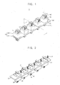
- FIG. 1 is a perspective view illustrating a lamp socket in accordance with an exemplary embodiment of the present invention.
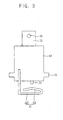
- FIG. 2 is a perspective view illustrating a rear portion of the lamp socket shown in FIG. 1.
- a lamp socket fixes a plurality of lamps to a receiving container to apply a lamp driving voltage to the lamps.
- the lamps supply a display panel with light.
- the lamp socket 5 includes a socket housing 10 and a plurality of power supply members 50.
- the socket housing 10 may be formed through an injection molding process.
- the socket housing 10 includes a plurality of connecting holes 41 extended in a vertical direction.
- the socket housing 10 may further include a connecting part 20 and a plurality of lamp holders 40.
- the connecting part 20 may have a plate shape extended in a longitudinal direction.
- a plurality of first fixing portions may be formed on a lower surface of the connecting part 20.
- the first fixing portions may include a plurality of fixing hooks 21 spaced apart from each other by a constant distance.
- the fixing hooks 21 may be combined with fixing holes formed through the receiving container.
- Each of the lamp holders 40 may be protruded from an upper surface of the connecting part 20 by a first height.
- the lamp holders 40 are interposed between the fixing hooks 21.
- the lamp holders 40 may be protruded from the lower surface of the connecting part 20 by a second height that is smaller than the first height.
- Each of the lamp holders 40 includes four lamp holding sidewalls and a lamp holding upper plate connected to the four lamp holding sidewalls.
- the connecting hole 41 is formed through the upper plate of the lamp holder 40.
- an aligning part may be formed under the lamp holder 40, and may include an aligning protrusion 33.
- the aligning protrusion 33 may be protruded from the lower surface of the connecting part 20.
- the aligning protrusion 33 guides a power supply substrate disposed under the lamp holder 40 to align an output terminal of the power supply substrate.
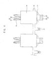
- FIG. 3 is a cross-sectional view taken along a line I-I' shown in FIG. 1.
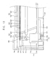
- FIG. 4 is a cross-sectional view taken along a line II-II' shown in FIG. 1.
- each of the power supply members 50 is inserted into each of the connecting holes 41.
- the power supply member 50 may include, for example, metal.
- the power supply member 50 may include, for example, a plurality of integrated lamp connecting parts 55 and 56 and/or a plurality of inverter connecting parts 51.
- the lamp connecting parts 55 and 56 apply the lamp driving voltage to an electrode portion of a lamp.
- the power supply member 50 includes two lamp connecting parts 55 and 56.
- the lamp connecting parts 55 and 56 may include a first lamp connecting part 55 and a second lamp connecting part 56 opposite to the first lamp connecting part 55.
- the first and second lamp connecting parts 55 and 56 are exposed toward an upper portion of the connecting hole 41, and face each other.
- the power supply member 50 may further include a conductive line in the connecting hole 41.
- the first and second connecting parts 55 and 56 may be electrically connected to each other through the conductive line.
- the first and second lamp connecting parts 55 and 56 may have a substantially symmetric shape with respect to a central line passing through the connecting hole 41.
- Each of the first and second connecting parts 55 and 56 may have a clamp shape.
- Each of the first and second connecting parts 55 and 56 may include a catching portion 57 and a contact portion 58.
- the catching portion 57 is extended in the vertical direction, and is protruded from an upper portion of the connecting hole 41.
- the contact portion 58 is bent from an upper end of the catching portion 57, and is extended toward the connecting hole 41.
- the contact portions 58 of the first and second lamp connecting parts 55 and 56 face each other. For example, a distance between the contact portions 58 of the first and second lamp connecting parts 55 and 56 may be decreased, as a distance from an upper portion of the connecting hole 41 may be decreased.
- a holding protrusion 59 may be formed on an upper portion of the catching portion 57.
- the holding protrusion 59 may be combined with a groove formed on the externally provided fixing element so that the externally provided fixing element is not removed from the first and second connecting parts 55 and 56.
- the first and second connecting parts 55 and 56 may have various shapes.
- the inverter connecting part 51 is exposed through a lower portion of the connecting hole 41.
- the inverter connecting part 51 may make contact with the output terminal of the power supply substrate.
- the inverter connecting part 51 may have one of a variety of shapes.
- the inverter connecting part 51 may have a spring shape, such as, for example, a leaf spring shape, so that the inverter connecting part 51 makes secure contact with the output terminal by using elasticity of the spring.
- the inverter connecting part 51 may include a supporting portion 52 and an electric power receiving portion 53.
- the supporting portion 52 is electrically connected to the conductive line that is electrically connected to the first and second lamp connecting parts 55 and 56, and is protruded from the lower surface of the connecting part 20.
- the supporting portion 52 is bent to face the lower surface of the lamp holder 40.
- the electric power receiving portion 53 is bent from an end portion of the supporting portion 52 to overlap the supporting portion 52.
- the electric power receiving portion 53 may have a convex shape with respect to the supporting portion 52.
- the electric power receiving portion 53 is elastically deformed based on an externally provided pressure so that the electric power receiving portion 53 is securely connected to the output terminal.
- FIG. 5 is a perspective view illustrating a lamp socket in accordance with an exemplary embodiment of the present invention.
- the lamp socket 105 that is integrated includes a socket housing 110 and a plurality of power supply members 150.
- the lamp socket 105 of FIG. 5 is substantially the same as the lamp socket 5 of FIGS. 1 to 4 at least except for a socket housing 110.
- the same reference numerals will be used to refer to the same or like parts as those described in FIGS. 1 to 4.
- the socket housing 110 includes a connecting part 120 and a lamp holder 140.
- the connecting part 120 has a plate shape extending in a longitudinal direction of the lamp socket 105.
- the lamp holder 140 is protruded from an upper surface of the connecting part 120 by a first height
- the connecting part 120 is protruded from a lower surface of the connecting part 120 by a second height that is smaller than the first height.
- the socket housing 110 may have a quadrangular parallelepiped shape.
- the socket housing 110 may have a rectangular parallelepiped shape.
- the socket housing 110 of FIG. 5 is substantially the same as the socket housing 10 of FIGS. 1 to 4 at least except for the shape of the socket housing 10.
- a plurality of connecting holes 141 is formed on an upper portion of the lamp holder 140, and passes through the lamp holder 140 in the vertical direction.
- a plurality of fixing hooks may be formed between the connecting holes 141.
- FIG. 6 is an exploded perspective view illustrating a backlight assembly in accordance with an exemplary embodiment of the present invention.
- the backlight assembly 300 includes a receiving container 310, a plurality of lamps 350, a power supply substrate 330 and a plurality of lamp sockets 405.
- the lamp sockets 405 are integrated.
- the receiving container 310 includes a bottom plate 311, a first sidewall 313, a second sidewall 315, a third sidewall 317 and a fourth sidewall 319.
- the first, second, third and fourth sidewalls 313, 315, 317 and 319 are protruded from sides of the bottom plate 311 to form a receiving space.
- the first and second sidewalls 313 and 315 face each other.
- the third and fourth sidewalls 317 and 319 face each other, and are connected between the first and second sidewalls 313 and 315.
- a stepped portion is formed on an upper portion of the first, second, third and fourth sidewalls 313, 315, 317 and 319.
- a plurality of openings 312 are formed on the bottom plate 311 adjacent to the first and second sidewalls 313 and 315.
- a second fixing portion may be formed between the openings 312.
- the second fixing portion may include a plurality of fixing holes 314.
- the lamps 350 are aligned on the bottom plate 311 to generate light.
- the lamps 350 may be aligned substantially parallel with each other so that a longitudinal direction of the lamps 350 may be substantially parallel with the third and fourth sidewalls 317 and 319.
- Each of the lamps 350 includes a lamp body and an electrode portion.
- the lamp body may have a cylindrical shape, and a discharge gas may be injected into the lamp body.
- the discharge gas may include argon and mercury.
- the electrode portion is on an end portion of the lamp body.
- the electrode portion may include a discharge electrode and a lead wire.
- the discharge electrode may be disposed in the lamp body, and the lead wire is extended from the discharge electrode toward an exterior to the lamp body.
- the lamp 350 may include an external electrode fluorescent lamp (EEFL) having various characteristics such as high brightness, low manufacturing cost, low power consumption, etc.
- EEFL external electrode fluorescent lamp
- a plurality of EEFLs may be driven by a single power supply unit.
- the backlight assembly 300 may further include a reflecting plate 340.
- the reflecting plate 340 is disposed on the bottom plate 311 of the receiving container 310 to reflect the light generated from the lamps 350 toward an upper portion of the backlight assembly 300.
- FIG. 7 is an enlarged perspective view illustrating the backlight assembly shown in FIG. 6.
- FIG. 8 is a perspective view illustrating a rear portion of the backlight assembly shown in FIG. 7.
- the lamp socket 405 are aligned on the bottom plate 311 along the first and second sidewalls 313 and 315.
- the lamp socket 405 adjacent to the first sidewall 313 is substantially the same as the lamp socket 405 adjacent to the second sidewall 315.
- any further explanation concerning the lamp socket 405 adjacent to the second sidewall 315 will be omitted.
- the lamp socket 405 of FIGS. 7 and 8 is substantially the same as the lamp socket 5 of FIGS. 1 to 4.
- Each of the lamp sockets 405 includes a socket housing 410 and a plurality of power supply members 450.
- the socket housing 410 includes a connecting part 420 and a plurality of lamp holders 440.
- the lamp holders 440 that are protruded from a lower surface of the connecting part 420 are received in the openings 312 that are formed through the bottom plate 311.
- the connecting part 420 is supported by a bottom surface of the bottom plate 311, and a plurality of fixing hooks that are formed on the lower surface of the lamp holder 440 is inserted into the fixing holes 314, respectively.
- the socket housing 410 is fixed to the bottom plate 311.
- the lamp holders 440 that are protruded from an upper surface of the connecting part 420 are disposed in the receiving space of the receiving container 310.
- the inverter connecting part 451 is exposed from a rear surface of the bottom plate 311.
- FIG. 9 is a plan view illustrating a rear surface of the backlight assembly shown in FIG. 6.
- the power supply substrate 330 is on the rear surface of the bottom plate 311, and generates a lamp driving voltage.
- the power supply substrate 330 may further include a printed circuit board (PCB) and a power supply element mounted on the PCB.
- PCB printed circuit board
- a side of the power supply substrate 330 is inserted into a space between the lower surface of the lamp holder 440 and the inverter connecting part 451.
- the side of the power supply substrate 330 includes a plurality of output terminals corresponding to the inverter connecting parts 451, respectively.
- conductive lines formed on the PCB may be partially exposed to form the output terminals.
- a second aligning part corresponding to a first aligning part formed on the lower surface of the lamp holder 440 may be formed adjacent to the output terminals.
- the first and second aligning parts may be an aligning protrusion and an aligning hole 335, respectively.
- a plurality of grooves may also be formed on the side of the power supply substrate between the output terminals when viewed from a plane.
- the side of the power supply substrate may have a convex and concave shape when viewed from the plane.
- the output terminals are formed on the rear surface of the power supply substrate 330.
- the output terminals may be formed on the upper surface of the power supply substrate 330.
- the output terminals may also be formed on the upper and rear surfaces of the power supply substrate 330.
- FIG. 10 is a cross-sectional view taken along a line III-III' shown in FIG. 6.
- FIG. 11 is a cross-sectional view taken along a line IV-IV' shown in FIG. 6.
- the aligning protrusion 433 formed on the lower surface of the lamp holder 440 is inserted into the aligning hole 335 formed through the power supply substrate 330.
- the output terminal 331 makes contact with the inverter connecting part 451.
- An electric power receiving portion 453 of the inverter connecting part 451 is elastically deformed to make contact with the output terminal 331.
- the power supply member 450 is electrically connected to the power supply substrate 330.
- the backlight assembly 300 may further include a protecting case 345 that protects the power supply substrate 330 and blocks electromagnetic interference.
- a lead wire 355 disposed on an end portion of a lamp body 351 may be interposed between a first lamp connecting part 455 and a second lamp connecting part 456 that are protruded from an upper portion of a connecting hole 441.
- the lead wire 355 may make contact with the first and second lamp connecting parts 455 and 456.
- the lead wire 355 may be spaced apart from the first and second lamp connecting parts 455 and 456.
- the backlight assembly 300 may further include a plurality of side covers 370 and optical sheets 380.
- Each of the side covers 370 is disposed on each of the first and second sidewalls 313 and 315 to cover the lamp sockets 405.
- the side covers 370 protect the lamp sockets 405.
- the side cover 370 presses the first and second lamp connecting parts 455 and 456 so that each of the first and second lamp connecting parts 455 and 456 makes contact with the lead wire 355. Therefore, the side cover 370 may improve reliability of electric contact between the lead wire 355 and the first and second lamp connecting parts 455 and 456.
- the side cover 370 includes a side portion 371 and an upper portion 375.
- the side portion 371 of the side cover 370 faces the first sidewall 313 and makes contact with the bottom plate 311.
- a plurality of guiding grooves are formed on an edge of the side portion 371 corresponding to the lamps 350.
- the upper portion 375 is extended from an upper side of the side portion 371 to face the bottom plate 311.
- the upper portion 375 may overlap a stepped portion that is formed on the first sidewall 313.
- a plurality of fixing portions 377 may be formed on a rear surface of the upper portion 375, and a stepped portion may be formed on the upper surface of the upper portion 375.
- the fixing portions 377 correspond to the lamp holders 440, respectively.
- a fixing recess may be formed on an end portion of each of the fixing portions 377. An edge of the fixing recess may have a hook shape.
- a holding protrusion 459 that is formed on each of the first and second lamp connecting parts 455 and 456 is supported by the fixing recess of the fixing portion 377 so that the first and second lamp connecting parts 455 and 456 are supported by the fixing recess.
- the lamps 350 are electrically connected to the power supply substrate 330 through the lamp socket 405.
- the optical sheets 380 may improve optical characteristics of the light generated from the lamps 350.
- the optical sheets 380 include a diffusion plate 381, a diffusion sheet 383 and a prism sheet 385 that are stacked in sequence.
- the diffusion plate 381, the diffusion sheet 383 and the prism sheet 385 are supported by the stepped portions formed on the third sidewall 317, the fourth sidewall 319 and the side cover 370.
- the optical sheets 380 may further include a plurality of prism sheets 385 and/or a brightness enhancement sheet (not shown).
- the diffusion plate 381 diffuses the light generated from the lamps 350 to increase luminance uniformity of the light.
- the diffusion sheet 383 also diffuses the diffused light passed through the diffusion plate-381.
- the prism sheet 385 guides the diffused light toward a front direction of the backlight assembly 300, thereby improving a luminance when viewed from a plane.
- the lamps 350 may be electrically connected to the power supply substrate 330 by using only the socket housing 410 and the power supply member 450.
- the number of elements of the lamp socket can be decreased.
- FIG. 12 is an exploded perspective view illustrating a display device in accordance with an exemplary embodiment of the present invention.
- FIG. 13 is a cross-sectional view taken along a line V-V' shown in FIG. 12.
- the display device 600 includes a receiving container 610, a lamp socket 705, a power supply substrate 630, a plurality of lamps 650, a plurality of side covers 670, optical sheets 680 and a display panel 780.
- the display device 600 may further include a plurality of lamp sockets 705 that are integrated.
- the receiving container 610, the lamp socket 705, the power supply substrate 630, the lamps 650, the side covers 670 and the optical sheets 680 of FIGS. 12 and 13 are substantially the same as in FIGS. 6 to 11.
- the same reference numerals will be used to refer to the same or like parts as those described in FIGS. 6 to 11 and any further explanation concerning the above elements will be omitted.
- the display device 600 may further include a middle frame 760.
- the middle frame 760 covers a peripheral portion of the optical sheets 680, and is combined with the receiving container 610.
- the display panel 780 displays an image based on light passed through the optical sheets 680.
- the display panel 780 includes a first substrate 781, a second substrate 783 and a liquid crystal layer (not shown).
- the second substrate 783 faces the first substrate 781.
- the liquid crystal layer is interposed between the first and second substrates 781 and 783.
- the display device 600 may further include a panel PCB 785 and a connecting film 787.
- the panel PCB 785 applies panel driving signals to the display panel 787.
- the connecting film 787 is electrically connected between the first substrate 781 and the panel PCB 785.
- the display device 600 may further include a top chassis 790 combined with the receiving container 610 or the middle frame 760, and has an opening through which an effective display region of the display panel 780 is exposed.
- a lamp socket includes a socket housing which is a single molded element and a power supply member to electrically connect lamps with a power supply substrate. Therefore, the lamps may be easily connected to the power supply substrate, and the number of elements of the lamp socket may be decreased.
- the lamps are combined with the power supply substrate through a removable combination.
- a wiring and soldering process for electric connection between the lead wiring of the lamp and the lamp socket, and between the lamp socket and the power supply substrate may be omitted, so that a manufacturing process for assembling the backlight assembly and the display device may be simplified.
- a power supply substrate having a defect may be easily removed from the lamp socket so that the power supply substrate may be substituted.
- the backlight assembly and the display device may be easily repaired.
Landscapes
- Physics & Mathematics (AREA)
- Nonlinear Science (AREA)
- Optics & Photonics (AREA)
- Crystallography & Structural Chemistry (AREA)
- Chemical & Material Sciences (AREA)
- General Physics & Mathematics (AREA)
- Mathematical Physics (AREA)
- Planar Illumination Modules (AREA)
- Fastening Of Light Sources Or Lamp Holders (AREA)
- Coupling Device And Connection With Printed Circuit (AREA)
- Arrangement Of Elements, Cooling, Sealing, Or The Like Of Lighting Devices (AREA)
- Liquid Crystal (AREA)
- Connecting Device With Holders (AREA)
- Multi-Conductor Connections (AREA)
Applications Claiming Priority (1)
| Application Number | Priority Date | Filing Date | Title |
|---|---|---|---|
| KR1020060069809A KR101318251B1 (ko) | 2006-07-25 | 2006-07-25 | 일체형 램프소켓, 이를 갖는 백라이트 어셈블리 및표시장치 |
Publications (3)
| Publication Number | Publication Date |
|---|---|
| EP1883138A2 true EP1883138A2 (de) | 2008-01-30 |
| EP1883138A3 EP1883138A3 (de) | 2009-12-09 |
| EP1883138B1 EP1883138B1 (de) | 2011-01-05 |
Family
ID=38709031
Family Applications (1)
| Application Number | Title | Priority Date | Filing Date |
|---|---|---|---|
| EP07014463A Ceased EP1883138B1 (de) | 2006-07-25 | 2007-07-24 | Lampenfassung, Rückbeleuchtungsanordnung und Anzeigevorrichtung |
Country Status (7)
| Country | Link |
|---|---|
| US (3) | US7549881B2 (de) |
| EP (1) | EP1883138B1 (de) |
| JP (1) | JP5143490B2 (de) |
| KR (1) | KR101318251B1 (de) |
| CN (1) | CN101126499B (de) |
| DE (1) | DE602007011695D1 (de) |
| TW (1) | TWI400846B (de) |
Cited By (2)
| Publication number | Priority date | Publication date | Assignee | Title |
|---|---|---|---|---|
| EP1906493A2 (de) | 2006-09-28 | 2008-04-02 | Samsung Electronics Co., Ltd. | Lampenfassung, Rückbeleuchtungsanordnung damit, Anzeigevorrichtung damit und Verfahren zur Montage eines Lampenmoduls |
| EP2239623A1 (de) * | 2009-04-07 | 2010-10-13 | Samsung Electronics Co., Ltd. | Flüssigkristallanzeigevorrichtung |
Families Citing this family (23)
| Publication number | Priority date | Publication date | Assignee | Title |
|---|---|---|---|---|
| KR101256185B1 (ko) * | 2007-01-25 | 2013-04-19 | 삼성디스플레이 주식회사 | 램프 소켓 가이드와 이를 구비한 램프 유닛 및 백라이트어셈블리 |
| KR101328662B1 (ko) * | 2006-11-14 | 2013-11-14 | 삼성디스플레이 주식회사 | 인버터 어셈블리, 이를 포함하는 백라이트 어셈블리 및이를 포함하는 액정 표시 장치 |
| CN101680640B (zh) * | 2007-06-11 | 2011-08-03 | 夏普株式会社 | 背光源装置、显示装置和电视接收机 |
| KR101334023B1 (ko) * | 2007-08-17 | 2013-11-28 | 삼성디스플레이 주식회사 | 램프 소켓, 이를 갖는 백라이트 어셈블리 및 상기 백라이트어셈블리를 갖는 표시장치 |
| TWI350931B (en) * | 2007-09-12 | 2011-10-21 | Au Optronics Corp | Backlight structure |
| JP4985292B2 (ja) * | 2007-10-04 | 2012-07-25 | 船井電機株式会社 | バックライト機構 |
| US20110007229A1 (en) * | 2008-02-27 | 2011-01-13 | Sharp Kabushiki Kaisha | Lighting device, display device and television receiver |
| KR101502914B1 (ko) * | 2008-04-11 | 2015-03-16 | 삼성디스플레이 주식회사 | 백라이트 어셈블리, 이를 포함하는 액정표시장치 및 조립방법 |
| KR100866372B1 (ko) * | 2008-04-15 | 2008-11-03 | 김우일 | 액정표시장치의 백라이트와 인버터의 결합구조 |
| KR101494209B1 (ko) * | 2008-05-09 | 2015-02-17 | 삼성디스플레이 주식회사 | 램프 가이드 프레임, 이를 갖는 커넥팅 모듈, 백라이트어셈블리 및 백라이트 어셈블리의 제조방법 |
| TWI376551B (en) * | 2008-05-14 | 2012-11-11 | Hannstar Display Corp | Backlight module, liquid crystal display device and method for manufacturing the backlight module |
| KR101322313B1 (ko) * | 2008-06-17 | 2013-10-25 | 엘지디스플레이 주식회사 | 액정표시장치 |
| WO2010021189A1 (ja) * | 2008-08-20 | 2010-02-25 | シャープ株式会社 | 照明装置、表示装置及びテレビ受信装置 |
| TWI387699B (zh) * | 2008-10-28 | 2013-03-01 | Chunghwa Picture Tubes Ltd | 燈座 |
| US8794786B2 (en) * | 2009-02-25 | 2014-08-05 | Sharp Kabushiki Kaisha | Lighting device, display device and television receiver |
| US20110298992A1 (en) * | 2009-03-13 | 2011-12-08 | Sharp Kabushiki Kaisha | Lighting device, display device and television receiver |
| US20100238621A1 (en) * | 2009-03-20 | 2010-09-23 | Tracy Mark S | Insert-molded conductor |
| TWM370104U (en) * | 2009-05-14 | 2009-12-01 | Chunghwa Picture Tubes Ltd | Backlight component fixing mechanism and related backlight module |
| TWD142734S (zh) * | 2010-02-12 | 2011-09-11 | 日本航空電子工業股份有限公司 | 背光用連接材 |
| US10050423B1 (en) * | 2017-02-07 | 2018-08-14 | Microsoft Technology Licensing, Llc | Cable-retention device assembly |
| KR102496259B1 (ko) * | 2018-02-08 | 2023-02-07 | 현대자동차주식회사 | 다중 단자 터미널 |
| CN208076752U (zh) * | 2018-04-20 | 2018-11-09 | 京东方科技集团股份有限公司 | 背光模组和显示装置 |
| TWI790796B (zh) * | 2021-11-01 | 2023-01-21 | 凡甲科技股份有限公司 | 電連接器 |
Family Cites Families (20)
| Publication number | Priority date | Publication date | Assignee | Title |
|---|---|---|---|---|
| US5720625A (en) * | 1992-06-06 | 1998-02-24 | Vossloh Schwabe Gmbh | Electrical clamping terminal arrangement |
| JP3455062B2 (ja) * | 1997-05-30 | 2003-10-06 | 京セラ株式会社 | コネクタ部材 |
| JP2001043715A (ja) * | 1999-07-30 | 2001-02-16 | Howa Bussan Kk | 平面照明装置 |
| KR100754775B1 (ko) * | 2001-03-10 | 2007-09-03 | 삼성전자주식회사 | 커넥터 및 이를 갖는 백라이트 어셈블리용 램프 유닛,그리고 액정 표시 장치 |
| CN2554846Y (zh) * | 2002-07-24 | 2003-06-04 | 佛山市石湾区柏联照明电器厂 | 带弹性接口的一体化直流供电微型光管支架 |
| KR100774579B1 (ko) * | 2002-10-25 | 2007-11-09 | 삼성전자주식회사 | 백라이트 어셈블리 및 이를 갖는 액정표시장치 |
| JP4189997B2 (ja) * | 2003-03-26 | 2008-12-03 | Tdk株式会社 | バックライトユニット |
| JP3932285B2 (ja) * | 2003-05-06 | 2007-06-20 | 日本航空電子工業株式会社 | ランプ保持構造 |
| JP2004349040A (ja) * | 2003-05-21 | 2004-12-09 | Nec Lcd Technologies Ltd | バックライト装置及び液晶表示装置 |
| KR100573783B1 (ko) | 2003-07-30 | 2006-04-25 | 유승명 | 액정표시장치의 백라이트 유닛과 램프 접속 방법 |
| TWM248097U (en) * | 2003-10-01 | 2004-10-21 | Zippy Tech Corp | Lamp frame structure of electroluminescent cathode lamp tube |
| JP2005150056A (ja) * | 2003-11-20 | 2005-06-09 | Funai Electric Co Ltd | 液晶表示装置用バックライト装置 |
| JP4017588B2 (ja) * | 2003-11-27 | 2007-12-05 | Tdk株式会社 | バックライトユニット |
| JP2005259370A (ja) * | 2004-03-09 | 2005-09-22 | Avenir Electronics International Co Ltd | 蛍光管用コネクタ装置 |
| KR101001973B1 (ko) * | 2004-04-12 | 2010-12-17 | 삼성전자주식회사 | 백라이트 어셈블리 및 이를 갖는 표시 장치 |
| KR20060019654A (ko) | 2004-08-28 | 2006-03-06 | 삼성전자주식회사 | 백라이트 어셈블리 및 이를 갖는 액정표시장치 |
| KR101065655B1 (ko) | 2004-09-09 | 2011-09-20 | 삼성전자주식회사 | 백 라이트 어셈블리 및 이를 갖는 액정 표시 장치 |
| JP2006120428A (ja) * | 2004-10-21 | 2006-05-11 | Jst Mfg Co Ltd | Eefl用コネクタ |
| TWI249880B (en) * | 2005-04-15 | 2006-02-21 | Coretronic Corp | Light source and connector |
| KR101183447B1 (ko) * | 2005-06-30 | 2012-09-17 | 엘지디스플레이 주식회사 | 액정표시장치용 반사시트 및 이를 이용한백라이트어셈블리와 액정표시장치모듈 |
-
2006
- 2006-07-25 KR KR1020060069809A patent/KR101318251B1/ko not_active Expired - Fee Related
-
2007
- 2007-07-24 US US11/782,318 patent/US7549881B2/en not_active Expired - Fee Related
- 2007-07-24 TW TW096126927A patent/TWI400846B/zh not_active IP Right Cessation
- 2007-07-24 EP EP07014463A patent/EP1883138B1/de not_active Ceased
- 2007-07-24 DE DE602007011695T patent/DE602007011695D1/de active Active
- 2007-07-24 JP JP2007192425A patent/JP5143490B2/ja not_active Expired - Fee Related
- 2007-07-25 CN CN2007101494437A patent/CN101126499B/zh not_active Expired - Fee Related
-
2009
- 2009-06-08 US US12/480,024 patent/US7789687B2/en not_active Expired - Fee Related
-
2010
- 2010-08-26 US US12/869,458 patent/US7967623B2/en not_active Expired - Fee Related
Cited By (5)
| Publication number | Priority date | Publication date | Assignee | Title |
|---|---|---|---|---|
| EP1906493A2 (de) | 2006-09-28 | 2008-04-02 | Samsung Electronics Co., Ltd. | Lampenfassung, Rückbeleuchtungsanordnung damit, Anzeigevorrichtung damit und Verfahren zur Montage eines Lampenmoduls |
| EP1906493A3 (de) * | 2006-09-28 | 2009-11-11 | Samsung Electronics Co., Ltd. | Lampenfassung, Rückbeleuchtungsanordnung damit, Anzeigevorrichtung damit und Verfahren zur Montage eines Lampenmoduls |
| US7771106B2 (en) | 2006-09-28 | 2010-08-10 | Samsung Electronics Co., Ltd. | Lamp socket, backlight assembly having the same, display device having the same and method of assembling a lamp module |
| EP2239623A1 (de) * | 2009-04-07 | 2010-10-13 | Samsung Electronics Co., Ltd. | Flüssigkristallanzeigevorrichtung |
| US8659715B2 (en) | 2009-04-07 | 2014-02-25 | Samsung Electronics Co., Ltd. | Liquid crystal display apparatus |
Also Published As
| Publication number | Publication date |
|---|---|
| KR101318251B1 (ko) | 2013-10-15 |
| JP2008034386A (ja) | 2008-02-14 |
| US7549881B2 (en) | 2009-06-23 |
| CN101126499A (zh) | 2008-02-20 |
| KR20080009966A (ko) | 2008-01-30 |
| US7967623B2 (en) | 2011-06-28 |
| TWI400846B (zh) | 2013-07-01 |
| US20090257216A1 (en) | 2009-10-15 |
| TW200814470A (en) | 2008-03-16 |
| US20100321924A1 (en) | 2010-12-23 |
| JP5143490B2 (ja) | 2013-02-13 |
| US7789687B2 (en) | 2010-09-07 |
| US20080024068A1 (en) | 2008-01-31 |
| EP1883138B1 (de) | 2011-01-05 |
| EP1883138A3 (de) | 2009-12-09 |
| DE602007011695D1 (de) | 2011-02-17 |
| CN101126499B (zh) | 2011-09-14 |
Similar Documents
| Publication | Publication Date | Title |
|---|---|---|
| EP1883138B1 (de) | Lampenfassung, Rückbeleuchtungsanordnung und Anzeigevorrichtung | |
| EP1906493B1 (de) | Anzeigevorrichtung mit einer Lampenfassung | |
| KR101385226B1 (ko) | 램프 소켓, 이를 갖는 백라이트 어셈블리 및 표시장치 | |
| EP2026427B1 (de) | Lampenfassung, Rückbeleuchtungsanordnung damit und Anzeigevorrichtung damit | |
| KR101294012B1 (ko) | 램프홀더, 전원공급모듈, 이를 갖는 백라이트 어셈블리 및표시장치 | |
| TWI394915B (zh) | 燈座、具該燈座之背光總成及其組裝方法 | |
| KR101537712B1 (ko) | 백라이트 어셈블리 및 이의 조립 방법 | |
| EP2149814B1 (de) | Lichtspendende Einheit und damit versehene Anzeigevorrichtung | |
| US8736789B2 (en) | Slim LCD module and a socket therefor | |
| KR101532050B1 (ko) | 백라이트 어셈블리 및 이의 조립 방법 | |
| EP1995833B1 (de) | Rückbeleuchtungsvorrichtung und Flüssigkristallanzeige dafür | |
| KR20080032286A (ko) | 백라이트 어셈블리 및 이를 갖는 표시장치 |
Legal Events
| Date | Code | Title | Description |
|---|---|---|---|
| PUAI | Public reference made under article 153(3) epc to a published international application that has entered the european phase |
Free format text: ORIGINAL CODE: 0009012 |
|
| AK | Designated contracting states |
Kind code of ref document: A2 Designated state(s): AT BE BG CH CY CZ DE DK EE ES FI FR GB GR HU IE IS IT LI LT LU LV MC MT NL PL PT RO SE SI SK TR |
|
| AX | Request for extension of the european patent |
Extension state: AL BA HR MK YU |
|
| RIN1 | Information on inventor provided before grant (corrected) |
Inventor name: JANG, TAE-SEOK Inventor name: SHIN, SEUNG-HA Inventor name: CHUNG, DU-HWAN Inventor name: CHOI, JIN-SUNG Inventor name: CHO, JOO-WOAN Inventor name: KIM, DONG-HOON Inventor name: JANG, HYEON-YONG Inventor name: CHOI, SEONG-SIK |
|
| PUAL | Search report despatched |
Free format text: ORIGINAL CODE: 0009013 |
|
| AK | Designated contracting states |
Kind code of ref document: A3 Designated state(s): AT BE BG CH CY CZ DE DK EE ES FI FR GB GR HU IE IS IT LI LT LU LV MC MT NL PL PT RO SE SI SK TR |
|
| AX | Request for extension of the european patent |
Extension state: AL BA HR MK RS |
|
| 17P | Request for examination filed |
Effective date: 20091230 |
|
| 17Q | First examination report despatched |
Effective date: 20100201 |
|
| GRAP | Despatch of communication of intention to grant a patent |
Free format text: ORIGINAL CODE: EPIDOSNIGR1 |
|
| AKX | Designation fees paid |
Designated state(s): DE FR GB |
|
| GRAS | Grant fee paid |
Free format text: ORIGINAL CODE: EPIDOSNIGR3 |
|
| GRAA | (expected) grant |
Free format text: ORIGINAL CODE: 0009210 |
|
| AK | Designated contracting states |
Kind code of ref document: B1 Designated state(s): DE FR GB |
|
| REG | Reference to a national code |
Ref country code: GB Ref legal event code: FG4D |
|
| REF | Corresponds to: |
Ref document number: 602007011695 Country of ref document: DE Date of ref document: 20110217 Kind code of ref document: P |
|
| REG | Reference to a national code |
Ref country code: DE Ref legal event code: R096 Ref document number: 602007011695 Country of ref document: DE Effective date: 20110217 |
|
| PLBE | No opposition filed within time limit |
Free format text: ORIGINAL CODE: 0009261 |
|
| STAA | Information on the status of an ep patent application or granted ep patent |
Free format text: STATUS: NO OPPOSITION FILED WITHIN TIME LIMIT |
|
| 26N | No opposition filed |
Effective date: 20111006 |
|
| REG | Reference to a national code |
Ref country code: DE Ref legal event code: R097 Ref document number: 602007011695 Country of ref document: DE Effective date: 20111006 |
|
| REG | Reference to a national code |
Ref country code: FR Ref legal event code: TP Owner name: SAMSUNG DISPLAY CO. LTD, KR Effective date: 20130226 |
|
| REG | Reference to a national code |
Ref country code: GB Ref legal event code: 732E Free format text: REGISTERED BETWEEN 20130307 AND 20130313 |
|
| REG | Reference to a national code |
Ref country code: DE Ref legal event code: R082 Ref document number: 602007011695 Country of ref document: DE Representative=s name: DR. WEITZEL & PARTNER, DE |
|
| REG | Reference to a national code |
Ref country code: DE Ref legal event code: R081 Ref document number: 602007011695 Country of ref document: DE Owner name: SAMSUNG DISPLAY CO., LTD., KR Free format text: FORMER OWNER: SAMSUNG ELECTRONICS CO., LTD., SUWON-SI, KR Effective date: 20130422 Ref country code: DE Ref legal event code: R082 Ref document number: 602007011695 Country of ref document: DE Representative=s name: DR. WEITZEL & PARTNER, DE Effective date: 20130422 Ref country code: DE Ref legal event code: R081 Ref document number: 602007011695 Country of ref document: DE Owner name: SAMSUNG DISPLAY CO., LTD., YONGIN-CITY, KR Free format text: FORMER OWNER: SAMSUNG ELECTRONICS CO., LTD., SUWON-SI, GYEONGGI-DO, KR Effective date: 20130422 Ref country code: DE Ref legal event code: R082 Ref document number: 602007011695 Country of ref document: DE Representative=s name: DR. WEITZEL & PARTNER PATENT- UND RECHTSANWAEL, DE Effective date: 20130422 |
|
| REG | Reference to a national code |
Ref country code: FR Ref legal event code: PLFP Year of fee payment: 10 |
|
| REG | Reference to a national code |
Ref country code: FR Ref legal event code: PLFP Year of fee payment: 11 |
|
| PGFP | Annual fee paid to national office [announced via postgrant information from national office to epo] |
Ref country code: GB Payment date: 20170707 Year of fee payment: 11 Ref country code: DE Payment date: 20170706 Year of fee payment: 11 Ref country code: FR Payment date: 20170710 Year of fee payment: 11 |
|
| REG | Reference to a national code |
Ref country code: DE Ref legal event code: R119 Ref document number: 602007011695 Country of ref document: DE |
|
| GBPC | Gb: european patent ceased through non-payment of renewal fee |
Effective date: 20180724 |
|
| PG25 | Lapsed in a contracting state [announced via postgrant information from national office to epo] |
Ref country code: DE Free format text: LAPSE BECAUSE OF NON-PAYMENT OF DUE FEES Effective date: 20190201 Ref country code: GB Free format text: LAPSE BECAUSE OF NON-PAYMENT OF DUE FEES Effective date: 20180724 Ref country code: FR Free format text: LAPSE BECAUSE OF NON-PAYMENT OF DUE FEES Effective date: 20180731 |