EP1886376B1 - Circuit d'attenuation de micro-ondes - Google Patents
Circuit d'attenuation de micro-ondes Download PDFInfo
- Publication number
- EP1886376B1 EP1886376B1 EP06759889A EP06759889A EP1886376B1 EP 1886376 B1 EP1886376 B1 EP 1886376B1 EP 06759889 A EP06759889 A EP 06759889A EP 06759889 A EP06759889 A EP 06759889A EP 1886376 B1 EP1886376 B1 EP 1886376B1
- Authority
- EP
- European Patent Office
- Prior art keywords
- circuit
- node
- port
- quarter wave
- circuit node
- Prior art date
- Legal status (The legal status is an assumption and is not a legal conclusion. Google has not performed a legal analysis and makes no representation as to the accuracy of the status listed.)
- Expired - Lifetime
Links
Images


Classifications
-
- H—ELECTRICITY
- H01—ELECTRIC ELEMENTS
- H01P—WAVEGUIDES; RESONATORS, LINES, OR OTHER DEVICES OF THE WAVEGUIDE TYPE
- H01P1/00—Auxiliary devices
- H01P1/22—Attenuating devices
- H01P1/227—Strip line attenuators
Definitions
- Coaxial attenuators are too bulky and expensive to be implemented on many microwave systems.
- Distributed ferrite load material on transmission lines have difficulty in realizing repeatable and precise attenuation values because of inconsistencies in the manufacturing the bulk material.
- Couplers on airstripline are not practical to realize small and precise attenuation values because of difficulties in match due to the unequal even and odd modes association with that type of transmission line.
- Typical lumped element attenuator configurations utilize at minimum three resistors. Each resistor value should be held to very tight tolerances, e.g. on the order of 1 % or better. Often active laser trimming is employed to achieve these precise resistor values. Laser trimming is typically preformed on printed resistor-on-ceramic substrates. This operation is prohibited for many large microwave printed circuit boards using non-ceramic material (Teflon7 for example) because of the risk of damaging the board by the laser.
- Document DE 41 18 384 A1 shows a two-part attenuator circuit comprising a first and a second input/output port, a first and a second quarter wave transformer, first to third circuit nodes as well as a first resistive element and a complex element.
- a two-port microwave attenuator circuit comprising: a first input/output port and a second I/O port; a first quarter wave transformer connected between a first circuit node and a second circuit node; a second quarter wave transformer connected between said first circuit node and a third circuit node; a first resistive element connected between said second circuit node and said third circuit node; a second resistive element connected between said third circuit node and a circuit ground; a third quarter wave transformer connected between said second circuit node and a fourth circuit node; a fourth quarter wave transformer connected between a fifth circuit node and said fourth circuit node; a third resistive element connected between said second circuit node and said fifth circuit node; and a fourth resistive element connected between said fifth circuit node and circuit ground.
- FIG. 1A is a schematic diagram of an attenuator device for illustrative purposes.
- FIG. 1B is a schematic diagram of an alternate attenuator device for illustrative purposes.
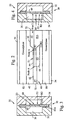
- FIG. 2 is a side view of an exemplary implementation of an attenuator device according to the schematic diagram of FIG. 1B , with an upper metal housing removed to illustrate the circuit and resistor pattern formed on a surface of the dielectric substrate.
- FIGS. 3 and 4 are respective left and right cross-sectional side view illustrations of the attenuator circuit of FIG. 2 .
- FIG. 5 illustrates in cross-section an exemplary embodiment of an attenuator fabricated in a channelized microstrip structure.
- FIG. 6 illustrates in cross-section an exemplary embodiment of an attenuator device fabricated in a channelized inverted microstrip structure.
- FIG. 7 illustrates in cross-section an exemplary embodiment of an attenuator device fabricated in a channelized double-sided air stripline structure.
- FIG. 8 illustrates in simplified schematic form an embodiment of an attenuator, wherein a back to back configuration allows a wider range of attenuation by a factor of two.
- FIG. 1A is a schematic diagram of an example of such an attenuator device.
- RF power P1 enter into port 1, and propagates to node a, where it is split between the two quarter wave transformers characterized by impedance Z1 and Z2.
- a quarter wave transformer is a length of transmission line, of length equivalent to one-quarter wavelength at an operating frequency, functioning to transform a first impedance at a first end of the transformer into a second impedance at the second end of the transformer.
- the characteristic impedance of the transmission line of the transformer is equal to the square root of the product of the first impedance and the second impedance.
- Quarter wave transformers are described, for example, in A Foundation for Microwave Engineering, @ R.E. Collin, Mcgraw-Hill, 1966, Chapter five .
- the impedance values of Z1 and Z2 determine the amount of power P2 that travels along the Z1 transformer, reaches node b and propagates through a quarter wave transformer of characteristic impedance Z3 into port 2.
- Quarter wave transformer Z3 transforms the impedance at node b to the impedance at port 3.
- the voltage at nodes b and c will be equal, so that no current flows through resistor R1.
- the proper selection of impedance values Z1, Z2, R2 and Z3, e.g. using even-odd mode analysis also realizes a good match at node A to the load impedance at port 2.
- Even-odd mode analyses are known in the art, e.g., J. Read and GJ.
- the power P3 that travels along the Z2 transformer reaches node c, and is dissipated in the resistor R2.
- the attenuation value of the attenuator circuit of FIG. 1 is determined by the ratio P2/P1. Choosing the proper resistor value R1 allows realization of the same attenuation value when power enter port 2 and exits port 1.
- a good match may also be realized at port 2 using even-odd mode analysis.
- the RF match using the configuration in FIG. 1 may be good across a 20 % frequency bandwidth at microwave frequencies in one exemplary embodiment, at an exemplary center frequency of 12.5 GHz.
- Both R1 and R2 are used as termination load resistors and do not impact the attenuation values as Z1 and Z2 do. It has been found that, for an exemplary embodiment, R1 and R2 may vary as much as 20 % without impacting the attenuation.
- the impedances presented at ports 1 and 2 may be 50 ohms.
- FIG. 1B is a schematic diagram of an alternate illustrative attenuator device.
- the bandwidth may be broadened, e.g. to up to 40 % at microwave frequencies in an exemplary embodiment.
- An exemplary embodiment of an microwave attenuator 20 illustrated in FIGS. 2-4 employs an etched strip transmission line pattern for each quarter wave transformer to determine an amount of attenuation through the device. Using the etched transmission line pattern can produce very precision impedance values which then result in very precise control of the attenuation values.
- only two resistors R1 and R2 are used to achieve a good match across the operating band, X band, for the device. These resistors can be printed onto the circuit board using resistive ink, mounted as discrete chips using, for example, a conventional solder or conductive epoxy attach method, or using a resistor product such as Ohmegaply (TM) marketed by Ohmega Corporation.
- TM Ohmegaply
- FIGS. 3 and 4 are left and right cross-sectional side view illustrations of the attenuator 20, showing the lower and upper metal housing structures 32 and 34. These structures may be fabricated of aluminum or other suitable metal. Alternatively, the structures may be fabricated of a plastic material coated with an outer layer of conductive material such as a metal. Each of the housing structures is generally U-shaped in cross-section, so that when the housing structures are joined together as shown in FIGS. 3 and 4 , an air cavity 36 is defined.
- the housing structure 42 has a recess 42A formed therein to receive a dielectric substrate 40.
- FIG. 2 is a side view of the device 20 taken with the upper metal housing 34 removed to illustrate the circuit and resistor pattern 60 formed on surface 40A of the dielectric substrate 40.
- the substrate can be fabricated from various dielectric materials, e.g. CuClad 250 (TM), ceramic, or 6010 Duroid (TM).
- the circuit pattern can be fabricated using photolithographic techniques, by way of example, wherein the surface 40A is first formed with a conductive layer, e.g. copper, covering the surface.
- the copper layer can be patterned using photolithographic techniques, selectively removing the copper layer to define a circuit pattern.
- the circuit pattern includes parallel, separated groundplane regions 80, 82 which contact surfaces of the metal housing structure 34. Matching groundplane regions may also be formed on the opposed surface of the substrate, opposite regions 80, 82.
- the circuit pattern includes a conductor strip 62 having a width selected to provide a characteristic transmission line impedance ZT. At the substrate edge, the strip forms a first I/O port 70.
- the circuit pattern also includes conductor strips 64 and 66, each having an effective electrical length of one quarter wavelength at a frequency within the operating band, e.g. at the center frequency of the operating band.
- the width of strip 64 is selected to provide a characteristic transmission line impedance Z1.
- the width of strip 66 is selected to provide a characteristic transmission line impedance Z2.
- the strips 62, 64 and 66 thus provide respective quarter-wave transformer sections.
- the conductor strip 66 has a tapered configuration at node B to reduce parasitic shunt capacitance and improve the match.
- a resistor R1 is connected at the opposite end of the strip 64 at node B. Resistor R1 is electrically connected at node B between the strip 64 and the strip 66. A resistor R2 is electrically connected between the end of strip 66 and the groundplane 80. These resistors R1, R2 may be printed onto the circuit board 40 or mounted as discrete chips using, for example, a conventional solder or conductive epoxy attach method.
- the circuit pattern 60 further includes a conductor strip 68 having a width selected to provide a characteristic transmission line impedance Z3.
- the conductor strip 68 has a tapered configuration at node B to reduce parasitic capacitance and improve the match.
- Strip 68 has a first end electrically connected at node B to the adjacent end of strip 64.
- a second end of strip 68 serves as the second I/O port 72 of the attenuator device.
- the resistors R1 and R2 and impedances ZT, Z1, Z2 and Z3 correspond to the similarly named resistors and impedances of the schematic diagram of FIG. 1B .
- the conductor strip 62 may be eliminated.
- the exemplary embodiment of an attenuator shown in FIGS. 2-4 is configured as a channelized single sided air stripline or suspended substrate stripline.
- the attenuator can be implemented in other transmission line structures.
- the attenuator can be implemented in channelized microstrip, channelized inverted microstrip, channelized double sided air stripline or high AQ@ air stripline, as illustrated in simplified form in FIGS. 5-7 , respectively.
- FIG. 5 illustrates in cross-section an exemplary embodiment of an attenuator 150 fabricated in a channelized microstrip structure.
- the attenuator 150 includes a bottom metal housing structure 152 and an upper metal housing structure 154.
- the bottom housing structure 152 includes a recessed region to receive the circuit board 40, which includes a circuit and resistor pattern 60 and groundplane regions formed on upper substrate surface 40A as in the embodiment of FIGS. 2-4 .
- the top housing structure 154 has an open channel formed therein to define an air cavity 158. The lower surface of the substrate is in contact with the lower housing structure 152.
- FIG. 6 illustrates in cross-section an exemplary embodiment of an attenuator device 170 fabricated in a channelized inverted microstrip structure.
- the attenuator 170 includes a housing structure 172 having a generally U shaped channel formed therein to define an air cavity 176.
- the circuit board 40 is inverted, so that the circuit and resistor pattern 60 is formed on surface 40A facing inwardly into the air cavity.
- the groundplane regions 80, 82 contact surfaces of a recessed region 172A of the housing structure 172.
- FIG. 7 illustrates in cross-section an exemplary embodiment of an attenuator device 180 fabricated in a channelized double-sided air stripline structure.
- the attenuator includes lower conductive housing structure 182 and upper conductive housing structure 184.
- the housing structures each form a general U-shaped configuration to define an air cavity 186 when the housing structures are assembled together as shown in FIG. 7 .
- a dielectric circuit board 40 is captured between the housing structures, and has groundplanes 80, 82 which contact mating surfaces of the upper housing structure 184.
- the board 40 has respective circuit and resistor patterns 60A and 60B formed on opposite sides of the board.
- the patterns 60A and 60B are identical to each other and to the circuit pattern 60 shown in FIG. 2 .
- FIG. 8 illustrates in simplified schematic form an embodiment of an attenuator 200, wherein a back to back configuration allows a wider range of attenuation, e.g., by a factor of two in an exemplary embodiment.
- the attenuator includes quarter-wavelength transformers ZT, Z1 and Z2 with nodes a, b and c.
- the attenuator further includes a second set of quarter-wavelength transformers Z3, Z4 and resistances R3, R4.
- Resistance R3 is connected between nodes b and d, at first ends of transformers Z4 and Z3.
- Resistance R4 is connected between node d and a groundplane.
- the opposite, second ends of the transformers Z3 and Z4 are connected at node e, which is connected by another quarter wave transformer Z5 to port 2 of the device 200.
- the attenuation is predicted to vary an exemplary embodiment by only 0.1 dB while the match is predicted to be better than 20 dB.
Landscapes
- Non-Reversible Transmitting Devices (AREA)
Abstract
Claims (12)
- Circuit d'atténuateur à hyperfréquences à deux ports, comprenant :un premier port d'entrée/sortie (E/S) (Port 1) et un deuxième port d'entrée/sortie (Port 2) ;un premier transformateur quart d'onde (Z1) connecté entre un premier noeud de circuit (a) et un deuxième noeud de circuit (b) ;un deuxième transformateur quart d'onde (Z2) connecté entre ledit premier noeud de circuit (a) et un troisième noeud de circuit (c) ;un premier élément résistif (R1) connecté entre ledit deuxième noeud de circuit (b) et ledit troisième noeud de circuit (c) ;un deuxième élément résistif (R2) connecté entre ledit troisième noeud de circuit et une masse de circuit ; caractérisé par :un troisième transformateur quart d'onde (Z4) connecté entre ledit deuxième noeud de circuit (b) et un quatrième noeud de circuit (e) ;un quatrième transformateur quart d'onde (Z3) connecté entre un cinquième noeud de circuit (d) et ledit quatrième noeud de circuit (e) ;un troisième élément résistif (R3) connecté entre ledit deuxième noeud de circuit (b) et ledit cinquième noeud de circuit (d) ;un quatrième élément résistif (R4) connecté entre ledit cinquième noeud de circuit et la masse de circuit.
- Circuit selon la revendication 1, dans lequel lesdits premier et deuxième transformateurs quart d'onde comprennent un substrat diélectrique (40) et un motif de bande conductrice (60) formé sur le substrat diélectrique.
- Circuit selon la revendication 1 ou la revendication 2, dans lequel lesdits premier et deuxième éléments résistifs sont des première et deuxième résistances à constantes localisées respectives.
- Circuit selon la revendication 2 ou la revendication 3, dans lequel lesdits premier et deuxième éléments respectifs sont fabriqués par impression des éléments résistifs sur le substrat diélectrique.
- Circuit selon la revendication 2 ou la revendication 3, dans lequel lesdits premier et deuxième éléments résistifs sont montés sur le substrat diélectrique sous la forme de première et deuxième pastilles individuelles.
- Circuit selon la revendication 2 ou la revendication 3, dans lequel lesdits premier et deuxième éléments résistifs sont montés sur le substrat diélectrique sous la forme de première et deuxième pastilles individuelles à l'aide d'une soudure ou d'un époxy conducteur.
- Circuit selon l'une quelconque des revendications précédentes, dans lequel ledit circuit est fabriqué sous la forme d'une ligne triplaque à air monoface canalisée (20).
- Circuit selon l'une quelconque des revendications 1 à 6, dans lequel le circuit comprend un circuit à microruban canalisé (150).
- Circuit selon l'une quelconque des revendications 1 à 6, dans lequel le circuit comprend un circuit à ligne triplaque à air double-face canalisée (180).
- Circuit selon la revendication 1, comprenant de plus un cinquième transformateur d'impédance quart d'onde (Z5) connecté entre ledit quatrième noeud de circuit (e) et ledit deuxième port d'entrée/sortie (Port 2).
- Circuit selon la revendication 10, comprenant de plus un sixième transformateur quart d'onde (ZT) connecté entre ledit premier noeud de circuit (a) et ledit premier port d'entrée/sortie (Port 1).
- Circuit selon l'une quelconque des revendications précédentes, dans lequel ledit circuit a une fréquence de fonctionnement dans une bande X/Ku.
Applications Claiming Priority (2)
| Application Number | Priority Date | Filing Date | Title |
|---|---|---|---|
| US11/143,147 US7276989B2 (en) | 2005-06-02 | 2005-06-02 | Attenuator circuit comprising a plurality of quarter wave transformers and lump element resistors |
| PCT/US2006/018828 WO2006132767A1 (fr) | 2005-06-02 | 2006-05-16 | Circuit d'attenuation de micro-ondes |
Publications (2)
| Publication Number | Publication Date |
|---|---|
| EP1886376A1 EP1886376A1 (fr) | 2008-02-13 |
| EP1886376B1 true EP1886376B1 (fr) | 2010-11-17 |
Family
ID=36791593
Family Applications (1)
| Application Number | Title | Priority Date | Filing Date |
|---|---|---|---|
| EP06759889A Expired - Lifetime EP1886376B1 (fr) | 2005-06-02 | 2006-05-16 | Circuit d'attenuation de micro-ondes |
Country Status (6)
| Country | Link |
|---|---|
| US (1) | US7276989B2 (fr) |
| EP (1) | EP1886376B1 (fr) |
| AU (1) | AU2006255759B2 (fr) |
| CA (1) | CA2605975C (fr) |
| DE (1) | DE602006018285D1 (fr) |
| WO (1) | WO2006132767A1 (fr) |
Families Citing this family (8)
| Publication number | Priority date | Publication date | Assignee | Title |
|---|---|---|---|---|
| US7276989B2 (en) * | 2005-06-02 | 2007-10-02 | Raytheon Company | Attenuator circuit comprising a plurality of quarter wave transformers and lump element resistors |
| DE102010020022A1 (de) * | 2010-05-10 | 2011-11-10 | Valeo Schalter Und Sensoren Gmbh | Fahrerassistenzeinrichtung für ein Fahrzeug, Fahrzeug und Verfahren zum Betreiben eines Radargeräts |
| DE102010046746B4 (de) | 2010-09-28 | 2023-08-10 | Continental Autonomous Mobility Germany GmbH | Elektrisches Dämpfungsglied |
| US9602091B1 (en) | 2015-12-03 | 2017-03-21 | Peregrine Semiconductor Corporation | Low phase shift, high frequency attenuator |
| US10771291B2 (en) | 2016-01-29 | 2020-09-08 | Hewlett Packard Enterprise Development Lp | Communication channel with tuning structure |
| US10347961B2 (en) * | 2016-10-26 | 2019-07-09 | Raytheon Company | Radio frequency interconnect systems and methods |
| JP7091862B2 (ja) * | 2018-06-14 | 2022-06-28 | 住友電工デバイス・イノベーション株式会社 | 可変減衰器 |
| US11043727B2 (en) | 2019-01-15 | 2021-06-22 | Raytheon Company | Substrate integrated waveguide monopulse and antenna system |
Family Cites Families (15)
| Publication number | Priority date | Publication date | Assignee | Title |
|---|---|---|---|---|
| US2409474A (en) * | 1943-05-13 | 1946-10-15 | Philco Corp | High-frequency attenuator and divider circuits |
| US3091743A (en) | 1960-01-04 | 1963-05-28 | Sylvania Electric Prod | Power divider |
| US3648200A (en) * | 1969-09-22 | 1972-03-07 | William H Harrison | Frequency selective attenuation apparatus |
| US3859609A (en) * | 1973-07-23 | 1975-01-07 | Texas Instruments Inc | Absorptive pin attenuators |
| US4394633A (en) * | 1981-04-28 | 1983-07-19 | Westinghouse Electric Corp. | Microstrip circuit with suspended substrate stripline regions embedded therein |
| GB2170358B (en) * | 1985-01-23 | 1988-09-21 | John Domokos | Microwave power divider |
| FI88564C (fi) | 1991-01-14 | 1993-05-25 | Nokia Mobile Phones Ltd | Styrbar hoegfrekvensdaempare |
| DE4118384A1 (de) * | 1991-06-05 | 1992-12-10 | Sueddeutscher Rundfunk | Daempfungsglied |
| DE9206124U1 (de) * | 1992-05-07 | 1992-09-10 | Süddeutscher Rundfunk, Anstalt des öffentlichen Rechts, 7000 Stuttgart | Dämpfungsglied |
| DE9206123U1 (de) * | 1992-05-07 | 1992-09-10 | Süddeutscher Rundfunk, Anstalt des öffentlichen Rechts, 7000 Stuttgart | Dämpfungsglied |
| US5506589A (en) | 1993-04-09 | 1996-04-09 | Hughes Aircraft Company | Monopulse array system with air-stripline multi-port network |
| US5345199A (en) * | 1993-08-12 | 1994-09-06 | The United States Of America As Represented By The Secretary Of The Army | Non-reflective limiter |
| US5712607A (en) * | 1996-04-12 | 1998-01-27 | Dittmer; Timothy W. | Air-dielectric stripline |
| JP3387452B2 (ja) | 1999-06-18 | 2003-03-17 | 株式会社村田製作所 | 誘電体線路減衰器、終端器および無線装置 |
| US7276989B2 (en) * | 2005-06-02 | 2007-10-02 | Raytheon Company | Attenuator circuit comprising a plurality of quarter wave transformers and lump element resistors |
-
2005
- 2005-06-02 US US11/143,147 patent/US7276989B2/en not_active Expired - Lifetime
-
2006
- 2006-05-16 CA CA2605975A patent/CA2605975C/fr not_active Expired - Lifetime
- 2006-05-16 AU AU2006255759A patent/AU2006255759B2/en not_active Expired
- 2006-05-16 EP EP06759889A patent/EP1886376B1/fr not_active Expired - Lifetime
- 2006-05-16 DE DE602006018285T patent/DE602006018285D1/de not_active Expired - Lifetime
- 2006-05-16 WO PCT/US2006/018828 patent/WO2006132767A1/fr not_active Ceased
Also Published As
| Publication number | Publication date |
|---|---|
| CA2605975C (fr) | 2014-12-09 |
| US7276989B2 (en) | 2007-10-02 |
| CA2605975A1 (fr) | 2006-12-14 |
| AU2006255759B2 (en) | 2009-10-29 |
| AU2006255759A1 (en) | 2006-12-14 |
| EP1886376A1 (fr) | 2008-02-13 |
| DE602006018285D1 (de) | 2010-12-30 |
| WO2006132767A1 (fr) | 2006-12-14 |
| US20060273863A1 (en) | 2006-12-07 |
Similar Documents
| Publication | Publication Date | Title |
|---|---|---|
| US7324060B2 (en) | Power divider having unequal power division and antenna array feed network using such unequal power dividers | |
| US6958662B1 (en) | Waveguide to stripline transition with via forming an impedance matching fence | |
| US5111165A (en) | Microwave coupler and method of operating same utilizing forward coupling | |
| EP0492357A1 (fr) | Coupleur 3dB en quadrature du type coplanaire | |
| US5922650A (en) | Method and structure for high power HTS transmission lines using strips separated by a gap | |
| AU2006255759B2 (en) | Microwave attenuator circuit | |
| US6087907A (en) | Transverse electric or quasi-transverse electric mode to waveguide mode transformer | |
| JP3112174B2 (ja) | 抵抗膜減衰器素子及びこれを組み込んだ伝送経路及びカスケード形減衰器 | |
| EP0417590B1 (fr) | Té magique planaire en forme de ligne à bande à air | |
| US7002433B2 (en) | Microwave coupler | |
| GB2170358A (en) | Microwave power divider | |
| US4419635A (en) | Slotline reverse-phased hybrid ring coupler | |
| JP2000252704A (ja) | 誘電体フィルタ | |
| KR20020036894A (ko) | 적층형 방향성 결합기 | |
| JPH044763B2 (fr) | ||
| KR100381545B1 (ko) | 적층형 방향성 결합기 | |
| EP1820236B1 (fr) | Dispositif de transmission | |
| JPH06204702A (ja) | マイクロ波フィルタ | |
| GB2189942A (en) | Transmission-line bias T | |
| JPH05283911A (ja) | 伝送線路 | |
| KR20020025311A (ko) | 적층형 방향성 결합기 | |
| JPH09199815A (ja) | マイクロ波回路 | |
| JP2004194176A (ja) | マイクロ波集積回路 |
Legal Events
| Date | Code | Title | Description |
|---|---|---|---|
| PUAI | Public reference made under article 153(3) epc to a published international application that has entered the european phase |
Free format text: ORIGINAL CODE: 0009012 |
|
| 17P | Request for examination filed |
Effective date: 20071205 |
|
| AK | Designated contracting states |
Kind code of ref document: A1 Designated state(s): DE ES FR GB SE |
|
| RBV | Designated contracting states (corrected) |
Designated state(s): DE ES FR GB SE |
|
| DAX | Request for extension of the european patent (deleted) | ||
| 17Q | First examination report despatched |
Effective date: 20091223 |
|
| GRAP | Despatch of communication of intention to grant a patent |
Free format text: ORIGINAL CODE: EPIDOSNIGR1 |
|
| GRAS | Grant fee paid |
Free format text: ORIGINAL CODE: EPIDOSNIGR3 |
|
| GRAA | (expected) grant |
Free format text: ORIGINAL CODE: 0009210 |
|
| AK | Designated contracting states |
Kind code of ref document: B1 Designated state(s): DE ES FR GB SE |
|
| REG | Reference to a national code |
Ref country code: GB Ref legal event code: FG4D |
|
| REF | Corresponds to: |
Ref document number: 602006018285 Country of ref document: DE Date of ref document: 20101230 Kind code of ref document: P |
|
| REG | Reference to a national code |
Ref country code: SE Ref legal event code: TRGR |
|
| PG25 | Lapsed in a contracting state [announced via postgrant information from national office to epo] |
Ref country code: ES Free format text: LAPSE BECAUSE OF FAILURE TO SUBMIT A TRANSLATION OF THE DESCRIPTION OR TO PAY THE FEE WITHIN THE PRESCRIBED TIME-LIMIT Effective date: 20110228 |
|
| PLBE | No opposition filed within time limit |
Free format text: ORIGINAL CODE: 0009261 |
|
| STAA | Information on the status of an ep patent application or granted ep patent |
Free format text: STATUS: NO OPPOSITION FILED WITHIN TIME LIMIT |
|
| 26N | No opposition filed |
Effective date: 20110818 |
|
| REG | Reference to a national code |
Ref country code: DE Ref legal event code: R097 Ref document number: 602006018285 Country of ref document: DE Effective date: 20110818 |
|
| REG | Reference to a national code |
Ref country code: FR Ref legal event code: PLFP Year of fee payment: 11 |
|
| REG | Reference to a national code |
Ref country code: FR Ref legal event code: PLFP Year of fee payment: 12 |
|
| REG | Reference to a national code |
Ref country code: FR Ref legal event code: PLFP Year of fee payment: 13 |
|
| P01 | Opt-out of the competence of the unified patent court (upc) registered |
Effective date: 20230530 |
|
| PGFP | Annual fee paid to national office [announced via postgrant information from national office to epo] |
Ref country code: DE Payment date: 20250423 Year of fee payment: 20 |
|
| PGFP | Annual fee paid to national office [announced via postgrant information from national office to epo] |
Ref country code: GB Payment date: 20250423 Year of fee payment: 20 |
|
| PGFP | Annual fee paid to national office [announced via postgrant information from national office to epo] |
Ref country code: FR Payment date: 20250423 Year of fee payment: 20 |
|
| PGFP | Annual fee paid to national office [announced via postgrant information from national office to epo] |
Ref country code: SE Payment date: 20250423 Year of fee payment: 20 |