EP1887549A2 - Verfahren und Vorrichtung zur Ansteuerung eines AMOLED mit variabler Steuerspannung - Google Patents
Verfahren und Vorrichtung zur Ansteuerung eines AMOLED mit variabler Steuerspannung Download PDFInfo
- Publication number
- EP1887549A2 EP1887549A2 EP07111202A EP07111202A EP1887549A2 EP 1887549 A2 EP1887549 A2 EP 1887549A2 EP 07111202 A EP07111202 A EP 07111202A EP 07111202 A EP07111202 A EP 07111202A EP 1887549 A2 EP1887549 A2 EP 1887549A2
- Authority
- EP
- European Patent Office
- Prior art keywords
- driving
- driving voltage
- amoled
- cell
- frame
- Prior art date
- Legal status (The legal status is an assumption and is not a legal conclusion. Google has not performed a legal analysis and makes no representation as to the accuracy of the status listed.)
- Ceased
Links
- 238000000034 method Methods 0.000 title claims description 26
- 229920001621 AMOLED Polymers 0.000 title claims description 5
- 230000003247 decreasing effect Effects 0.000 claims description 6
- 230000033001 locomotion Effects 0.000 abstract description 12
- 239000011159 matrix material Substances 0.000 abstract description 7
- 239000003990 capacitor Substances 0.000 description 8
- 230000000007 visual effect Effects 0.000 description 5
- 238000010586 diagram Methods 0.000 description 4
- 210000004556 brain Anatomy 0.000 description 3
- 230000006870 function Effects 0.000 description 3
- OAICVXFJPJFONN-UHFFFAOYSA-N Phosphorus Chemical compound [P] OAICVXFJPJFONN-UHFFFAOYSA-N 0.000 description 2
- 238000005286 illumination Methods 0.000 description 2
- 230000004466 optokinetic reflex Effects 0.000 description 2
- 230000002688 persistence Effects 0.000 description 2
- 230000011664 signaling Effects 0.000 description 2
- 230000001360 synchronised effect Effects 0.000 description 2
- 230000007423 decrease Effects 0.000 description 1
- 230000000694 effects Effects 0.000 description 1
- 230000004424 eye movement Effects 0.000 description 1
- 230000002349 favourable effect Effects 0.000 description 1
- 230000006872 improvement Effects 0.000 description 1
- 230000009191 jumping Effects 0.000 description 1
- 238000004020 luminiscence type Methods 0.000 description 1
- 239000000463 material Substances 0.000 description 1
- 230000007246 mechanism Effects 0.000 description 1
- 230000004048 modification Effects 0.000 description 1
- 238000012986 modification Methods 0.000 description 1
- 230000011514 reflex Effects 0.000 description 1
- 230000004044 response Effects 0.000 description 1
- 210000001525 retina Anatomy 0.000 description 1
Images





Classifications
-
- G—PHYSICS
- G09—EDUCATION; CRYPTOGRAPHY; DISPLAY; ADVERTISING; SEALS
- G09G—ARRANGEMENTS OR CIRCUITS FOR CONTROL OF INDICATING DEVICES USING STATIC MEANS TO PRESENT VARIABLE INFORMATION
- G09G3/00—Control arrangements or circuits, of interest only in connection with visual indicators other than cathode-ray tubes
- G09G3/20—Control arrangements or circuits, of interest only in connection with visual indicators other than cathode-ray tubes for presentation of an assembly of a number of characters, e.g. a page, by composing the assembly by combination of individual elements arranged in a matrix no fixed position being assigned to or needed to be assigned to the individual characters or partial characters
- G09G3/22—Control arrangements or circuits, of interest only in connection with visual indicators other than cathode-ray tubes for presentation of an assembly of a number of characters, e.g. a page, by composing the assembly by combination of individual elements arranged in a matrix no fixed position being assigned to or needed to be assigned to the individual characters or partial characters using controlled light sources
- G09G3/30—Control arrangements or circuits, of interest only in connection with visual indicators other than cathode-ray tubes for presentation of an assembly of a number of characters, e.g. a page, by composing the assembly by combination of individual elements arranged in a matrix no fixed position being assigned to or needed to be assigned to the individual characters or partial characters using controlled light sources using electroluminescent panels
- G09G3/32—Control arrangements or circuits, of interest only in connection with visual indicators other than cathode-ray tubes for presentation of an assembly of a number of characters, e.g. a page, by composing the assembly by combination of individual elements arranged in a matrix no fixed position being assigned to or needed to be assigned to the individual characters or partial characters using controlled light sources using electroluminescent panels semiconductive, e.g. using light-emitting diodes [LED]
- G09G3/3208—Control arrangements or circuits, of interest only in connection with visual indicators other than cathode-ray tubes for presentation of an assembly of a number of characters, e.g. a page, by composing the assembly by combination of individual elements arranged in a matrix no fixed position being assigned to or needed to be assigned to the individual characters or partial characters using controlled light sources using electroluminescent panels semiconductive, e.g. using light-emitting diodes [LED] organic, e.g. using organic light-emitting diodes [OLED]
- G09G3/3225—Control arrangements or circuits, of interest only in connection with visual indicators other than cathode-ray tubes for presentation of an assembly of a number of characters, e.g. a page, by composing the assembly by combination of individual elements arranged in a matrix no fixed position being assigned to or needed to be assigned to the individual characters or partial characters using controlled light sources using electroluminescent panels semiconductive, e.g. using light-emitting diodes [LED] organic, e.g. using organic light-emitting diodes [OLED] using an active matrix
-
- G—PHYSICS
- G09—EDUCATION; CRYPTOGRAPHY; DISPLAY; ADVERTISING; SEALS
- G09G—ARRANGEMENTS OR CIRCUITS FOR CONTROL OF INDICATING DEVICES USING STATIC MEANS TO PRESENT VARIABLE INFORMATION
- G09G2300/00—Aspects of the constitution of display devices
- G09G2300/08—Active matrix structure, i.e. with use of active elements, inclusive of non-linear two terminal elements, in the pixels together with light emitting or modulating elements
- G09G2300/0809—Several active elements per pixel in active matrix panels
- G09G2300/0842—Several active elements per pixel in active matrix panels forming a memory circuit, e.g. a dynamic memory with one capacitor
-
- G—PHYSICS
- G09—EDUCATION; CRYPTOGRAPHY; DISPLAY; ADVERTISING; SEALS
- G09G—ARRANGEMENTS OR CIRCUITS FOR CONTROL OF INDICATING DEVICES USING STATIC MEANS TO PRESENT VARIABLE INFORMATION
- G09G2300/00—Aspects of the constitution of display devices
- G09G2300/08—Active matrix structure, i.e. with use of active elements, inclusive of non-linear two terminal elements, in the pixels together with light emitting or modulating elements
- G09G2300/0809—Several active elements per pixel in active matrix panels
- G09G2300/0842—Several active elements per pixel in active matrix panels forming a memory circuit, e.g. a dynamic memory with one capacitor
- G09G2300/0861—Several active elements per pixel in active matrix panels forming a memory circuit, e.g. a dynamic memory with one capacitor with additional control of the display period without amending the charge stored in a pixel memory, e.g. by means of additional select electrodes
- G09G2300/0866—Several active elements per pixel in active matrix panels forming a memory circuit, e.g. a dynamic memory with one capacitor with additional control of the display period without amending the charge stored in a pixel memory, e.g. by means of additional select electrodes by means of changes in the pixel supply voltage
-
- G—PHYSICS
- G09—EDUCATION; CRYPTOGRAPHY; DISPLAY; ADVERTISING; SEALS
- G09G—ARRANGEMENTS OR CIRCUITS FOR CONTROL OF INDICATING DEVICES USING STATIC MEANS TO PRESENT VARIABLE INFORMATION
- G09G2310/00—Command of the display device
- G09G2310/06—Details of flat display driving waveforms
- G09G2310/066—Waveforms comprising a gently increasing or decreasing portion, e.g. ramp
-
- G—PHYSICS
- G09—EDUCATION; CRYPTOGRAPHY; DISPLAY; ADVERTISING; SEALS
- G09G—ARRANGEMENTS OR CIRCUITS FOR CONTROL OF INDICATING DEVICES USING STATIC MEANS TO PRESENT VARIABLE INFORMATION
- G09G2320/00—Control of display operating conditions
- G09G2320/02—Improving the quality of display appearance
- G09G2320/0261—Improving the quality of display appearance in the context of movement of objects on the screen or movement of the observer relative to the screen
-
- G—PHYSICS
- G09—EDUCATION; CRYPTOGRAPHY; DISPLAY; ADVERTISING; SEALS
- G09G—ARRANGEMENTS OR CIRCUITS FOR CONTROL OF INDICATING DEVICES USING STATIC MEANS TO PRESENT VARIABLE INFORMATION
- G09G2320/00—Control of display operating conditions
- G09G2320/06—Adjustment of display parameters
- G09G2320/0626—Adjustment of display parameters for control of overall brightness
Definitions
- the present invention relates to a method for driving a cell of an AMOLED (Active Matrix Organic Light Emitting Display) including the steps of applying a driving voltage to the cell and applying a luminance control signal to the cell during a pregiven time frame. Furthermore, the present invention relates to an apparatus for driving such a cell.
- AMOLED Active Matrix Organic Light Emitting Display
- Fig. 1 it comprises :
- each digital video information sent by the digital processing unit 5 is converted by the column drivers 4 into a current whose amplitude is directly proportional to the video level. This current is provided to the appropriate cell 2 of the matrix 1.
- the digital video information sent by the digital processing unit 5 is converted by the column drivers 4 into a voltage whose amplitude is proportional to the square of the video level. This current or voltage is provided to the appropriate cell 2 of the matrix 1.
- an OLED is current driven so that each voltage based driven system is based on a voltage to current converter to achieve appropriate cell lighting.
- the row driver 3 has a quite simple function since it only has to apply a selection line by line. It is more or less a shift register.
- the column driver 4 represents the real active part and can be considered as a high level digital to analog converter.
- the displaying of a video information with such a structure of AMOLED is symbolized in Fig. 2.
- the input signal is forwarded to the digital processing unit that delivers, after internal processing, a timing signal for row selection to the row driver synchronized with the data sent to the column driver 4.
- the data transmitted to the column driver 4 are either parallel or serial.
- the column driver 4 disposes of a reference signalling delivered by a separate reference signalling device 6. This component 6 delivers a set of reference voltages in case of voltage driven circuitry or a set of reference currents in case of current driven circuitry. The highest reference is used for the white and the lowest for the smallest gray level. Then, the column driver 4 applies to the matrix cells 2 the voltage or current amplitude corresponding to the data to be displayed by the cells 2.
- the grayscale level is defined by storing during one frame an analog value in a capacitor located at the current pixel location. This value is kept by the pixel up to the next refresh coming with the next frame. In that case, the video value is rendered in a fully analog way and stays stable during the whole frame.
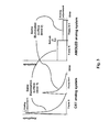
- This concept is different from that of a CRT which works with an impulse as depicted in Figure 3.
- the selected pixel of a CRT will receive a pulse coming from the beam and generating on the phosphor a lighting peak that decreases rapidly depending on the phosphor persistence.
- a new peak will be produced exactly one frame later (e.g. 20ms later for 50hz, 16,67ms later for 60Hz and so on).
- the luminance of the current pixel is stable during the whole frame period.
- the value of the pixel will be updated only at the beginning of each frame.
- the surface of the illumination curves for level 1 and level 2 are equal between CRT and AMOLED if the same power management system is used. All amplitudes being controlled in an analog way.
- a motion-picture film is a strip of discrete, still pictures but produces the visual impression of continuous movement.
- effects of apparent movement (called the visual phi phenomenon) depend on the persistence of vision: visual response outlasts a stimulus by a fraction of a second.
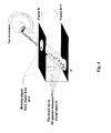
- Figure 4 illustrates the eye movement in the case of displaying a gray disk moving on a black background.
- the eye From a frame N to a following frame N+1 the eye will perform a movement as shown in the Figure. Simultaneously, it will integrate objects lying on a time line. The brain tries to fill spaces between the visual objects of the frames.
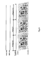
- Figure 5 shows the difference between the picture rendition of a gray moving circle on a dark background for a CRT and an AMOLED.
- the impulse rendition suits very well to the visual phi phenomenon. Indeed, the brain has no problem to identify the CRT information as a continuous movement.
- the principle structure of a cell is already known from Figure 1.
- the TFT T2 can be realized with a n-channel or a p-channel.
- Figure 6 shows a comparison between p and n type TFT for this AMOLED application. The main differences reside in the global driving voltages as described below:
- the row driver will open the transistor T1 by applying a high level (n-channel) or a low level (p-channel) signal via the "Line (k)". Then the signal level given on the "Column” at this time will be stored in the capacitor C as illustrated in Figure 7.
- the example given in Figure 7 is based on a QVGA display with 240 lines and 320 pixels (RGB ⁇ 960 cells).
- the driving voltage between Vdd and GND is fixed during the whole time (values are given here only as example).
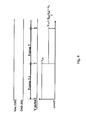
- the vertical synchronization pulse V is high at the starting of each frame. This signal launches the addressing of the display (row or line pulse) given for row 0 to row 239 where the corresponding data signals are given on the 960 columns line by line.
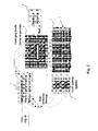
- the video information can be seen as shown in Figure 8. It shows that pictures are displayed one after the other based on the V synchronization signal with a delay from lines to lines due to the addressing operation (the time needed for changing the capacitor value is not negligible).
- one given pixel from the first line (e.g. value 255 in frame T and 128 in frame T+1) will have the behavior illustrated in Figure 9.
- This Figure shows the same example as presented in Figure 4. As already explained this way of video rendition will introduce a lack of sharpness during the movement.
- the object of the present invention to provide a method and apparatus for driving a cell of an AMOLED so that the sharpness impression during the movement of an object on the AMOLED is improved.
- This object is solved by a method for driving a cell of an AMOLED including the steps of applying a driving voltage to said cell and applying a luminance control signal to said cell during a pregiven time frame, as well as varying said driving voltage within said time frame according to a predefined triangle function of time.
- an apparatus for driving a cell of an AMOLED including driving means for applying a driving voltage and a luminance control signal to said cell during a pregiven time frame, as well as controlling means for varying said driving voltage within said time frame according to a predefined triangle function of time.
- the time frame defined above may correspond to the time of a signal frame for displaying a picture on the AMOLED. Moreover, the time frame may also correspond to a sub-frame of the luminance control signal, i.e. the video signal.
- the above described method or apparatus can be combined with a sub-frame coding technique of the international patent application WO 05/104074 .
- the invention can also be combined with the concept presented in the European patent application 05292759.7 introduced above.
- the driving voltage is reduced to a pregiven addressing time interval within the above-defined time frame.
- the emission of light is deactivated during the addressing operation.
- the driving voltage may be increased or decreased continuously within the time frame. Such slope of the driving voltage simulates a CRT, so that the sharpness impression of the picture displayed on the AMOLED is enhanced.
- the driving voltage may be increased and decreased continuously within in the time frame. This driving principle also ensures that the maximum light emission only appears in a part of the frame.
- the driving voltage may be given by a driving potential and a ground potential, and the ground potential may be modified for varying the driving voltage.
- the driving potential may be modified for varying the driving voltage. The appropriate modification of the driving voltage depends on the hardware of a cell used.
- the present invention aims on presenting a new AMOLED gray scale rendition method overcoming the problem on motion rendition issues.
- the idea is to have a lighting emission which is more similar to that of a CRT.
- the driving voltage will be modified as presented in the examples below.
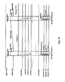
- Figure 10 illustrates a first concept for triangle driving in case of n-channel TFTs.
- the driving potential Vdd is kept constant and a driving voltage is given by the difference of the driving potential Vdd and the ground potential GND.
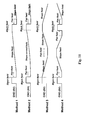
- Figure 12 illustrates the real behavior for method 1 of Figure 11 for the example given in Figure 10.
- the maximum video level of frame T-1 is 255.
- the video level of frame T for the given cell is 128, i.e. in the present case of the video level of frame T-1.
- the brightness of the cell is reduced during frame T until zero as the ground potential GND increases. If the slope field would be characterized by a curve like in method 2 of Figure 11, the brightness of a cell during the frame would go down degresssively.
- Figure 13 shows the brightness behavior of a cell for method 3 of Figure 11. Similar to Figure 12 the brightness of the cell is mirror-inverted to the ground potential GND. Here, the brightness curve has the shape of a pyramid.
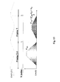
- FIG. 14 shows the principle applied to the p-channel transistor.
- the black fields are achieved by setting Vdd below V th .
- the flat fields are achieved by maintaining Vdd at the maximum value. The only difference is that the changes of Vdd reflect directly the changes of luminance whereas in n-channel type, it is mirror-inverted.
- the ground potential GND is kept constant.
- the line and column driving signals are identical to those of the example of Figure 10.
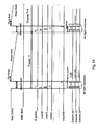
- Figure 15 illustrates an implementation of the inventive solution.
- the input signal 11 is forwarded to the standard OLED processing unit 12 and driving block 13 as usual.
- the standard OLED unit 13 produces row driving data for a row driver 14 of an AMOLED 15.
- the standard OLED driving unit 13 outputs column driving data to a column driver 16 of the AMOLED 15.
- a control unit 17 receives timing information from the input via the standard OLED processing unit 12. With this timing information, the control unit 17 controls a standard OLED processing block 12 and the standard OLED driving unit 13. Furthermore, the control unit 17 controls a reference signal unit 18 by programming specific reference voltages or reference currents input to the column driver 16.
- the inventive display device shown in Figure 15 includes a waveform generator 18 for controlling the ground potential GND and/or the driving potential Vdd.
- the waveform generator 18 itself is controlled and synchronized by the control block 17 to suit with a addressing operation.
- the waveform generator is adapted to vary GND and/or Vdd within the time period of a frame or sub-frame.
- the control block 17 together with the waveform generator 18 are now responsible for the whole inventive driving concept.
Landscapes
- Engineering & Computer Science (AREA)
- Physics & Mathematics (AREA)
- Computer Hardware Design (AREA)
- General Physics & Mathematics (AREA)
- Theoretical Computer Science (AREA)
- Control Of Indicators Other Than Cathode Ray Tubes (AREA)
- Electroluminescent Light Sources (AREA)
Priority Applications (1)
| Application Number | Priority Date | Filing Date | Title |
|---|---|---|---|
| EP07111202A EP1887549A3 (de) | 2006-06-30 | 2007-06-27 | Verfahren und Vorrichtung zur Ansteuerung eines AMOLED mit variabler Steuerspannung |
Applications Claiming Priority (2)
| Application Number | Priority Date | Filing Date | Title |
|---|---|---|---|
| EP06300742A EP1873746A1 (de) | 2006-06-30 | 2006-06-30 | Verfahren und Vorrichtung zur Ansteuerung eines AMOLED mit variabler Steuerspannung |
| EP07111202A EP1887549A3 (de) | 2006-06-30 | 2007-06-27 | Verfahren und Vorrichtung zur Ansteuerung eines AMOLED mit variabler Steuerspannung |
Publications (2)
| Publication Number | Publication Date |
|---|---|
| EP1887549A2 true EP1887549A2 (de) | 2008-02-13 |
| EP1887549A3 EP1887549A3 (de) | 2009-03-18 |
Family
ID=38924727
Family Applications (1)
| Application Number | Title | Priority Date | Filing Date |
|---|---|---|---|
| EP07111202A Ceased EP1887549A3 (de) | 2006-06-30 | 2007-06-27 | Verfahren und Vorrichtung zur Ansteuerung eines AMOLED mit variabler Steuerspannung |
Country Status (1)
| Country | Link |
|---|---|
| EP (1) | EP1887549A3 (de) |
Cited By (1)
| Publication number | Priority date | Publication date | Assignee | Title |
|---|---|---|---|---|
| EP2701141A1 (de) * | 2012-08-23 | 2014-02-26 | BlackBerry Limited | Aktive Matrixpixelhelligkeitssteuerung |
Citations (1)
| Publication number | Priority date | Publication date | Assignee | Title |
|---|---|---|---|---|
| WO2006059737A1 (en) * | 2004-11-30 | 2006-06-08 | Semiconductor Energy Laboratory Co., Ltd. | Display device and driving method thereof, semiconductor device, and electronic apparatus |
Family Cites Families (3)
| Publication number | Priority date | Publication date | Assignee | Title |
|---|---|---|---|---|
| GB0218170D0 (en) * | 2002-08-06 | 2002-09-11 | Koninkl Philips Electronics Nv | Electroluminescent display devices |
| KR20040019207A (ko) * | 2002-08-27 | 2004-03-05 | 엘지.필립스 엘시디 주식회사 | 유기전계발광소자와 그의 구동장치 및 방법 |
| GB0316862D0 (en) * | 2003-07-18 | 2003-08-20 | Koninkl Philips Electronics Nv | Display device |
-
2007
- 2007-06-27 EP EP07111202A patent/EP1887549A3/de not_active Ceased
Patent Citations (1)
| Publication number | Priority date | Publication date | Assignee | Title |
|---|---|---|---|---|
| WO2006059737A1 (en) * | 2004-11-30 | 2006-06-08 | Semiconductor Energy Laboratory Co., Ltd. | Display device and driving method thereof, semiconductor device, and electronic apparatus |
Cited By (1)
| Publication number | Priority date | Publication date | Assignee | Title |
|---|---|---|---|---|
| EP2701141A1 (de) * | 2012-08-23 | 2014-02-26 | BlackBerry Limited | Aktive Matrixpixelhelligkeitssteuerung |
Also Published As
| Publication number | Publication date |
|---|---|
| EP1887549A3 (de) | 2009-03-18 |
Similar Documents
| Publication | Publication Date | Title |
|---|---|---|
| EP1743315B1 (de) | Verfahren zur graustufen-wiedergabe in einer am-oled | |
| US8462180B2 (en) | Method for grayscale rendition in an AM-OLED | |
| US11094251B2 (en) | Coding for avoiding motion artifacts | |
| US20220051620A1 (en) | Display device and method for driving thereof | |
| US20070146394A1 (en) | Display and driving method thereof | |
| US8054321B2 (en) | Display and driving method thereof | |
| US20080204374A1 (en) | Method and apparatus for driving an AMOLED with variable driving voltage | |
| EP1964092B1 (de) | Verfahren zur bildanzeige auf einer organischen lichtemittierenden anzeige und entsprechende vorrichtung | |
| CN101017637A (zh) | 显示装置 | |
| US7522130B2 (en) | Plasma display panel (PDP)—improvement of dithering noise while displaying less video levels than required | |
| US20110242067A1 (en) | Multii-scan analog sub-fields for sample and hold displays | |
| JP2023048342A (ja) | 電気光学装置、電子機器及び駆動方法 | |
| EP1914709A1 (de) | Verfahren zur Graustufenwiedergabe in einer Aktiv-Matrix-OLED-Anzeige |
Legal Events
| Date | Code | Title | Description |
|---|---|---|---|
| PUAI | Public reference made under article 153(3) epc to a published international application that has entered the european phase |
Free format text: ORIGINAL CODE: 0009012 |
|
| AK | Designated contracting states |
Kind code of ref document: A2 Designated state(s): AT BE BG CH CY CZ DE DK EE ES FI FR GB GR HU IE IS IT LI LT LU LV MC MT NL PL PT RO SE SI SK TR |
|
| AX | Request for extension of the european patent |
Extension state: AL BA HR MK YU |
|
| PUAL | Search report despatched |
Free format text: ORIGINAL CODE: 0009013 |
|
| AK | Designated contracting states |
Kind code of ref document: A3 Designated state(s): AT BE BG CH CY CZ DE DK EE ES FI FR GB GR HU IE IS IT LI LT LU LV MC MT NL PL PT RO SE SI SK TR |
|
| AX | Request for extension of the european patent |
Extension state: AL BA HR MK RS |
|
| 17Q | First examination report despatched |
Effective date: 20091001 |
|
| 17P | Request for examination filed |
Effective date: 20090831 |
|
| AKX | Designation fees paid |
Designated state(s): DE FR GB |
|
| RAP1 | Party data changed (applicant data changed or rights of an application transferred) |
Owner name: THOMSON LICENSING |
|
| STAA | Information on the status of an ep patent application or granted ep patent |
Free format text: STATUS: THE APPLICATION HAS BEEN REFUSED |
|
| 18R | Application refused |
Effective date: 20120415 |