EP1887601A1 - Plasmabildschirm - Google Patents
Plasmabildschirm Download PDFInfo
- Publication number
- EP1887601A1 EP1887601A1 EP07708245A EP07708245A EP1887601A1 EP 1887601 A1 EP1887601 A1 EP 1887601A1 EP 07708245 A EP07708245 A EP 07708245A EP 07708245 A EP07708245 A EP 07708245A EP 1887601 A1 EP1887601 A1 EP 1887601A1
- Authority
- EP
- European Patent Office
- Prior art keywords
- dielectric layer
- oxide
- electrodes
- dielectric
- pdp
- Prior art date
- Legal status (The legal status is an assumption and is not a legal conclusion. Google has not performed a legal analysis and makes no representation as to the accuracy of the status listed.)
- Withdrawn
Links
Images
Classifications
-
- H—ELECTRICITY
- H01—ELECTRIC ELEMENTS
- H01J—ELECTRIC DISCHARGE TUBES OR DISCHARGE LAMPS
- H01J11/00—Gas-filled discharge tubes with alternating current induction of the discharge, e.g. alternating current plasma display panels [AC-PDP]; Gas-filled discharge tubes without any main electrode inside the vessel; Gas-filled discharge tubes with at least one main electrode outside the vessel
- H01J11/20—Constructional details
- H01J11/34—Vessels, containers or parts thereof, e.g. substrates
- H01J11/38—Dielectric or insulating layers
-
- H—ELECTRICITY
- H01—ELECTRIC ELEMENTS
- H01J—ELECTRIC DISCHARGE TUBES OR DISCHARGE LAMPS
- H01J11/00—Gas-filled discharge tubes with alternating current induction of the discharge, e.g. alternating current plasma display panels [AC-PDP]; Gas-filled discharge tubes without any main electrode inside the vessel; Gas-filled discharge tubes with at least one main electrode outside the vessel
- H01J11/10—AC-PDPs with at least one main electrode being out of contact with the plasma
- H01J11/12—AC-PDPs with at least one main electrode being out of contact with the plasma with main electrodes provided on both sides of the discharge space
Definitions
- the present invention relates to a plasma display panel used in a display device, and the like.
- PDP plasma display panel
- 65-inch class televisions are commercialized.
- PDPs have been applied to full high-definition in which the number of scan lines is twice or more than that of a conventional NTSC method. Meanwhile, from the viewpoint of environmental problems, PDPs without containing a lead component have been demanded.
- a PDP basically includes a front panel and a rear panel.
- the front panel includes a glass substrate of sodium borosilicate glass produced by a float process; display electrodes each composed of striped transparent electrode and metal bus electrode formed on one principal surface of the glass substrate; a dielectric layer covering the display electrodes and functioning as a capacitor; and a protective layer made of magnesium oxide (MgO) formed on this dielectric layer.
- the rear panel includes a glass substrate; striped address electrodes formed on one principal surface of the glass substrate; a base dielectric layer covering the address electrodes; barrier ribs formed on the base dielectric layer; and phosphor layers formed between the barrier ribs and emitting red, green and blue light, respectively.
- the front panel and the rear panel are hermetically sealed so that their surfaces having electrodes face each other.
- Discharge gas of Ne-Xe is filled in discharge space participated by the barrier ribs at a pressure of 400 Torr to 600 Torr.
- the PDP realizes a color image display by selectively applying a video signal voltage to a display electrode so as to generate electric discharge, and exciting a phosphor layer of each color with ultraviolet ray generated by the electric discharge so as to emit red, green and blue light.
- a silver electrode for securing electric conductivity is used
- a low melting point glass material containing lead oxide as a main component is used.
- PDPs have been applied to full high-definition in which the number of scan lines is twice or more than that of a conventional NTSC method. With such a trend toward high definition, the number of scan lines is increased, and the number of display electrodes is increased. Furthermore, the interval between the display electrodes is reduced.
- a low melting point glass material such as bismuth oxide, which suppresses the reaction with a silver electrode, be used for a dielectric layer instead of using a lead component.
- a large amount of low melting point glass materials such as bismuth oxide is used for a dielectric layer
- the visible light transmittance of the dielectric layer is remarkably lowered.
- the amount of the low melting point glass material such as bismuth oxide is reduced in order to suppress the lowering of the visible light transmittance of the dielectric layer, the reaction with silver electrode cannot be suppressed sufficiently, which may cause coloring and insufficient insulation.
- a conventional dielectric layer without containing a lead component which has been proposed from the viewpoint of environmental problems, has had a problem that it is difficult to achieve both prevention of coloring and insufficient insulation and suppression of lowering of the visible light transmittance in the dielectric layer.
- the present invention addresses the problems discussed above, and aims to provide a PDP including a dielectric layer that does not contain a lead component, in which coloring and insufficient insulation of the dielectric layer are prevented and lowering of the visible light transmittance is suppressed even in a high definition display.
- the PDP of the present invention includes a front panel and a rear panel disposed facing each other and sealed together at the peripheries thereof with discharge space being provided therebetween.
- the front panel includes display electrodes, a dielectric layer and a protective layer formed on a glass substrate; and the rear panel includes electrodes, barrier ribs, and phosphor layers formed on a substrate.
- the display electrode contains at last silver.
- the dielectric layer includes a first dielectric layer covering the display electrodes and containing bismuth oxide, and a second dielectric layer covering the first dielectric layer and containing bismuth oxide.
- the thickness ratio of the second dielectric layer to the first dielectric layer is set to be not less than 1.3 and not more than 7.2.
- the dielectric layer of the PDP of the present invention includes a first dielectric layer covering the display electrodes, and a second dielectric layer covering the first dielectric layer and having a lower content of bismuth oxide than that of the first dielectric layer.
- the dielectric layer includes the first dielectric layer having a higher content of bismuth oxide in order to suppress the reaction with silver, and the second dielectric layer having a lower content of bismuth oxide in order to avoid the lowering of the visible light transmittance in the thickness ratio mentioned above, the first dielectric layer suppresses the reaction with silver and the second dielectric layer secures a necessary withstand voltage without lowering the visible light transmittance.
- the PDP including a dielectric layer, in which coloring and insufficient insulation of the dielectric layer are prevented and lowering of the visible light transmittance is suppressed.
- the first dielectric layer includes not less than 0.1 wt% and not more than 7 wt% of at least one of molybdenum oxide and tungsten oxide.
- molybdenum oxide and tungsten oxide are reacted with silver ions, so that it is possible to suppress the generation of silver colloid and bubbles.
- the second dielectric layer includes not less than 11 wt% and not more than 20 wt% of bismuth oxide.
- the visible light transmittance can be enhanced.
- the first dielectric layer and the second dielectric layer include at least one of zinc oxide, boron oxide, silicon oxide, aluminum oxide, calcium oxide, strontium oxide, and barium oxide.
- the PDP which includes a dielectric layer that is not deteriorated in withstand voltage performance and has high visible light transmittance and which is environmentally friendly and excellent in display quality.
- a PDP including a dielectric layer that does not contain a lead component in which coloring and insufficient insulation of the dielectric layer are prevented and the lowering of the visible light transmittance is suppressed even in a high definition display.
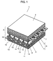
- Fig. 1 is a perspective view showing a structure of a PDP in accordance with an exemplary embodiment of the present invention.
- the basic structure of the PDP is the same as that of a general AC surface discharge PDP.
- PDP 1 includes front panel 2 and rear panel 10 disposed facing each other and hermetically sealed together at the peripheries thereof with a sealing material including a glass frit, and the like.
- Front panel 2 includes front glass substrate 3, etc.
- rear panel 10 includes rear glass substrate 11, etc.
- discharge gas such as neon (Ne) and xenon (Xe) is filled in at a pressure of 400 Torr to 600 Torr.
- plurality of band-like display electrodes 6 each composed of a pair of scan electrode 4 and sustain electrode 5 and black stripes (light blocking layers) 7 are disposed in parallel to each other.
- dielectric layer 8 functioning as a capacitor is formed so as to cover display electrodes 6 and black stripes (light blocking layers) 7. Furthermore, on the surface of dielectric layer 8, protective layer 9 made of, for example, magnesium oxide (MgO) is formed.
- MgO magnesium oxide
- a plurality of band-like address electrodes 12 are disposed in parallel to each other in the direction perpendicular to scan electrodes 4 and sustain electrodes 5 of front panel 2, and address electrodes 12 are covered with based dielectric layer 13.
- address electrodes 12 on dielectric layer 13 a plurality of barrier ribs 14 with a predetermined height for partitioning discharge space 16 are formed.
- phosphor layers 15 emitting red, blue and green light by ultraviolet ray are sequentially formed by coating.
- sustain electrodes 5 and address electrodes 12 intersect each other, discharge cells are formed.
- the discharge cells having red, blue and green phosphor layers 15 arranged in the direction of display electrode 6 function as pixel for color display.
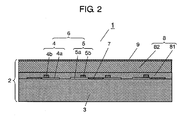
- Fig. 2 is a sectional view of front panel 2 showing a configuration of dielectric layer 8 of the PDP in accordance with an exemplary embodiment of the present invention.
- Fig. 2 is shown turned upside down with respect to Fig. 1 .
- display electrodes 6 each composed of scan electrode 4 and sustain electrode 5 and black stripes (light blocking layers) 7 are formed by patterning.
- Scan electrode 4 and sustain electrode 5 include transparent electrodes 4a and 5a made of indium tin oxide (ITO), tin oxide (SnO 2 ), or the like, and metal bus electrodes 4b and 5b formed on transparent electrodes 4a and 5a, respectively.
- Metal bus electrodes 4b and 5b are used for the purpose of providing conductivity in the longitudinal direction of transparent electrodes 4a and 5a and formed of a conductive material containing a silver material as a main component.
- Dielectric layer 8 includes at least two layers, that is, first dielectric layer 81 and second dielectric layer 82.
- First dielectric layer 81 is provided for covering transparent electrodes 4a and 5a, metal bus electrodes 4b and 5b, and black stripes (light blocking layers) 7 formed on front glass substrate 3.
- Second dielectric layer 82 is formed on first dielectric layer 81. Furthermore, on second dielectric layer 82, protective layer 9 is formed.
- Transparent electrodes 4a and 5a and metal bus electrodes 4b and 5b are formed by patterning by using, for example, a photolithography method.
- Transparent electrodes 4a and 5a are formed by, for example, a thin film process.
- Metal bus electrodes 4b and 5b are formed by firing paste including a silver material at a predetermined temperature and solidifying it.
- black stripe (light blocking layer) 7 is similarly formed by a method of screen printing of paste including a black pigment, or a method of forming a black pigment over the entire surface of the glass substrate, then carrying out patterning by a photolithography method, and firing thereof.
- a dielectric paste is coated on front glass substrate 3 by, for example, a die coating method so as to cover scan electrodes 4, sustain electrodes 5 and black stripes (light blocking layers) 7, thus forming a dielectric paste layer (dielectric material layer).
- dielectric paste is coated, it is stood still for a predetermined time. Thus, the surface of the coated dielectric paste is leveled and flattened. Thereafter, by firing and solidifying the dielectric paste layer, dielectric layer 8 covering scan electrodes 4, sustain electrodes 5 and black stripes (light blocking layers) 7 is formed.
- the dielectric paste is a coating material including a dielectric material such as glass powder, a binder and a solvent.
- protective layer 9 made of magnesium oxide (MgO) is formed by a vacuum evaporation method.
- predetermined components for example, scan electrodes 4, sustain electrodes 5, black stripes (light blocking layers) 7, dielectric layer 8 and protective layer 9 are formed.
- front panel 2 is completed.
- rear panel 10 is formed as follows. Firstly, a material layer as components for address electrode 12 is formed on rear glass substrate 11 by a method of screen printing a paste including a silver material, or by a method of forming a metal film on the entire surface, followed by patterning by using a photolithography method. The material layer is fired at a predetermined temperature. Thus, address electrode 12 is formed.
- a dielectric paste is coated by a die coating method on rear glass substrate 11 on which address electrodes 12 are formed so as to cover address electrodes.
- a dielectric paste layer is formed.
- base dielectric layer 13 is formed.
- a dielectric paste is a coating material including a dielectric material such as glass powder, a binder and a solvent.
- barrier rib formation paste including materials for barrier ribs on base dielectric layer 13 and patterning it into a predetermined shape, a barrier rib material layer is formed, and then fired.
- barrier ribs 14 are formed.
- a method of patterning the barrier rib formation paste coated on base dielectric layer 13 may include a photolithography method and a sand blasting method.
- phosphor layer 15 is formed by coating a phosphor paste including phosphor materials between neighboring barrier ribs 14 on base dielectric layer 13 and on the side surface of barrier rib 14 and firing thereof. With the above-mentioned process, rear panel 10 having predetermined component members is completed on rear glass substrate 11.
- Discharge gas including neon, xenon, or the like, is filled in the discharge space.
- PDP 1 is formed.
- a dielectric material of first dielectric layer 81 includes the following material composition. That is to say, the material composition includes 25 wt% to 40 wt% of bismuth oxide (Bi 2 O 3 ), 27.5 wt% to 34 wt% of zinc oxide (ZnO), 17 wt% to 36 wt% of boron oxide (B 2 O 3 ), 1.4 wt% to 4.2 wt% of silicon oxide (SiO 2 ) and 0.5 wt% to 4.4 wt% of aluminum oxide (Al 2 O 3 ).
- the material composition includes 25 wt% to 40 wt% of bismuth oxide (Bi 2 O 3 ), 27.5 wt% to 34 wt% of zinc oxide (ZnO), 17 wt% to 36 wt% of boron oxide (B 2 O 3 ), 1.4 wt% to 4.2 wt% of silicon oxide (SiO 2 ) and 0.5 wt% to 4.4 wt% of aluminum oxide
- wt% to 13 wt% of at least one selected from calcium oxide (CaO), strontium oxide (SrO) and barium oxide (BaO) and 0.1 wt% to 7 wt% of at least one selected from molybdenum oxide (MoO 3 ) and tungsten oxide (WO 3 ) are included.
- MoO 3 molybdenum oxide
- tungsten oxide WO 3
- 0.1 wt% to 7 wt% of at least one selected from cerium oxide (CeO 2 ), copper oxide (CuO), manganese dioxide (MnO 2 ), chromium oxide (Cr 2 O 3 ), cobalt oxide (Co 2 O 3 ), vanadium oxide (V 2 O 7 ) and antimony oxide (Sb 2 O 3 ) may be included.
- the dielectric materials including these composition components are ground to have an average particle diameter of 0.5 ⁇ m to 2.5 ⁇ m by using a wet jet mill or a ball mill. Thus, dielectric material powder is formed. Then, 55 wt% to 70 wt% of this dielectric material powder and 30 wt% to 45 wt% of binder components are well kneaded by using three rolls to form a paste for the first dielectric layer to be used in die coating or printing.
- the binder component includes ethyl cellulose, or terpineol including 1 wt% to 20 wt% of acrylic resin, or butyl carbitol acetate.
- dioctyl phthalate, dibutyl phthalate, triphenyl phosphate, and tributyl phosphate may be added as a plasticizer, and glycerol monooleate, sorbitan sesquioleate, Homogenol (trademark of Kao Corporation), phosphate ester of an alkyl-allyl group, and the like, may be added as a dispersing agent, so that the printing property may be improved.
- this paste for the first dielectric layer is printed on front glass substrate 3 by a die coating method or a screen printing method so as to cover display electrode 6 and dried, followed by firing it at a temperature of 575°C to 590°C, that is, a little higher temperature than the softening temperature of the dielectric material.
- a dielectric material of second dielectric layer 82 includes the following material composition. That is to say, the material composition includes 11 wt% to 20 wt% of bismuth oxide (Bi 2 O 3 ), 26.1 wt% to 39.3 wt% of zinc oxide (ZnO), 23 wt% to 32.2 wt% of boron oxide (B 2 O 3 ), 1.0 wt% to 3.8 wt% of silicon oxide (SiO 2 ) and 0.1 wt% to 10.2 wt% of aluminum oxide (Al 2 O 3 ).
- the material composition includes 11 wt% to 20 wt% of bismuth oxide (Bi 2 O 3 ), 26.1 wt% to 39.3 wt% of zinc oxide (ZnO), 23 wt% to 32.2 wt% of boron oxide (B 2 O 3 ), 1.0 wt% to 3.8 wt% of silicon oxide (SiO 2 ) and 0.1 wt% to 10.2
- the dielectric materials including these composition components are ground to have an average particle diameter of 0.5 ⁇ m to 2.5 ⁇ m by using a wet jet mill or a ball mill. Thus, dielectric material powder is formed. Then, 55 wt% to 70 wt% of this dielectric material powder and 30 wt% to 45 wt% of binder components are well kneaded by using three rolls to form a paste for the second dielectric layer to be used in die coating or printing.
- the binder component includes ethyl cellulose, or terpineol including 1 wt% to 20 wt% of acrylic resin, or butyl carbitol acetate.
- dioctyl phthalate, dibutyl phthalate, triphenyl phosphate, and tributyl phosphate may be added as a plasticizer, and glycerol monooleate, sorbitan sesquioleate, Homogenol (trademark of Kao Corporation), phosphate ester of an alkyl-allyl group, and the like, may be added as a dispersing agent, so that the printing property may be improved.
- this paste for the second dielectric layer is printed on first dielectric layer 81 by a screen printing method or a die coating method and dried, followed by firing it at a temperature of 550°C to 590°C, that is, a little higher temperature than the softening temperature of the dielectric material.
- the film thickness of dielectric layer 8 is not more than 41 ⁇ m in total of first dielectric layer 81 and second dielectric layer 82 in order to secure the visible light transmittance.
- the content of bismuth oxide in first dielectric layer 81 is set to be 25 wt% to 40 wt%, which is higher than the content of bismuth oxide in second dielectric layer 82, in order to suppress the reaction between metal bus electrodes 4b and 5b and silver (Ag). Therefore, since the visible light transmittance of first dielectric layer 81 becomes lower than that of second dielectric layer 82, the film thickness of first dielectric layer 81 is set to be thinner than that of second dielectric layer 82.
- the content of bismuth oxide (Bi 2 O 3 ) is not more than 11 wt% in second dielectric layer 82 because the visible light transmittance is not easily lowered but bubbles tend to be generated in second dielectric layer 82. Furthermore, it is not preferable that the content is more than 20 wt% for the purpose of increasing the visible light transmittance.
- the film thickness of dielectric layer 8 is smaller, the effect of improving the panel brightness and reducing the discharge voltage can be achieved remarkably. However, if the film thickness of dielectric layer 8 is made to be too small, necessary withstand voltage cannot be obtained.
- first dielectric layer 81 covering metal bus electrodes 4b and 5b have a high content of bismuth oxide.
- dielectric layer 8 needs a predetermined film thickness. Therefore, second dielectric layer 82, which does not extremely reduce the visible light transmittance, has a low content of bismuth oxide and has a predetermined film thickness, is necessary.
- first dielectric layer 81 and second dielectric layer 82 satisfying the above-mentioned conditions are examined.
- the thickness ratio of second dielectric layer 82 to first dielectric layer 81 is not less than 1.3 and not more than 7.2. This is because when the thickness ratio is less than 1.3, necessary withstand voltage cannot be obtained, and when it is more than 7.2, the visible light transmittance is remarkably lowered.
- the reason why these dielectric materials suppress the coloring and generation of bubbles in first dielectric layer 81 is considered. That is to say, by adding molybdenum oxide (MoO 3 ) or tungsten oxide (WO 3 ) to a dielectric glass material containing bismuth oxide (Bi 2 O 3 ), it is known that compounds such as Ag 2 MoO 4 , Ag 2 Mo 2 O 7 , Ag2Mo 4 O 13 , Ag 2 WO 4 , Ag 2 W 2 O 7 , and Ag 2 W 4 O 13 are easily generated at a low temperature such as not more than 580°C.
- MoO 3 molybdenum oxide
- WO 3 tungsten oxide
- the firing temperature of dielectric layer 8 is in the range from 550°C to 590°C
- Ag ions (Ag + ) diffusing in dielectric layer 8 during firing react with molybdenum oxide (MoO 3 ) and tungsten oxide (WO 3 ) in dielectric layer 8, so that a stable compound is generated and stabilized. That is to say, since Ag ions (Ag + ) are not subjected to reduction reaction but stabilized, the ions do not coagulate and a colloid is not formed. Therefore, by the stabilization of Ag ions (Ag + ), since generation of oxygen associated with formation of silver (Ag) colloid is decreased. Consequently, the generation of bubbles in dielectric layer 8 is also decreased.
- the content of molybdenum oxide (MoO 3 ) or tungsten oxide (WO 3 ) in the dielectric glass material containing bismuth oxide (Bi 2 O 3 ) is made to be not less than 0.1 wt%. It is further preferable that the content is made to be not less than 0.1 wt% and not more than 7 wt%. In particular, it is not preferable that the content is not more than 0.1 wt% because the effect of suppressing coloring is reduced; and it is not preferable that the content is more than 7 wt% because coloring occurs in a dielectric glass material.
- first dielectric layer 81 that is brought into contact with metal bus electrode 4b and 5b made of a silver material suppresses the phenomenon of coloring and generation of bubbles
- second dielectric layer 82 formed on the first dielectric layer 81 realizes high visible light transmittance while securing the withstand voltage.
- generation of bubbles and coloring is extremely reduced and visible light transmittance is high.
- a PDP including such dielectric layer 8 can be realized.
- a PDP of the present invention includes a dielectric layer that is free from coloring or deterioration of the withstand voltage performance, and is environmentally friendly and excellent in display quality.
- the PDP of the present invention is useful for a large-screen display device.
Landscapes
- Physics & Mathematics (AREA)
- Engineering & Computer Science (AREA)
- Plasma & Fusion (AREA)
- Gas-Filled Discharge Tubes (AREA)
Applications Claiming Priority (2)
| Application Number | Priority Date | Filing Date | Title |
|---|---|---|---|
| JP2006036347A JP4089733B2 (ja) | 2006-02-14 | 2006-02-14 | プラズマディスプレイパネル |
| PCT/JP2007/052261 WO2007094239A1 (ja) | 2006-02-14 | 2007-02-08 | プラズマディスプレイパネル |
Publications (2)
| Publication Number | Publication Date |
|---|---|
| EP1887601A1 true EP1887601A1 (de) | 2008-02-13 |
| EP1887601A4 EP1887601A4 (de) | 2008-10-29 |
Family
ID=38371426
Family Applications (1)
| Application Number | Title | Priority Date | Filing Date |
|---|---|---|---|
| EP07708245A Withdrawn EP1887601A4 (de) | 2006-02-14 | 2007-02-08 | Plasmabildschirm |
Country Status (6)
| Country | Link |
|---|---|
| US (1) | US8072142B2 (de) |
| EP (1) | EP1887601A4 (de) |
| JP (1) | JP4089733B2 (de) |
| KR (1) | KR100948713B1 (de) |
| CN (1) | CN101326611B (de) |
| WO (1) | WO2007094239A1 (de) |
Cited By (4)
| Publication number | Priority date | Publication date | Assignee | Title |
|---|---|---|---|---|
| EP2144270A3 (de) * | 2008-07-07 | 2010-09-01 | Samsung SDI Co., Ltd. | Paste mit Aluminium zur Herstellung einer PDP-Elektrode, Herstellungsverfahren zur Herstellung der PDP-Elektrode mit der Paste und PDP-Elektrode, die mit diesem Verfahren hergestellt wurde |
| EP2144269A3 (de) * | 2008-07-07 | 2010-09-01 | Samsung SDI Co., Ltd. | Substratstruktur für eine Plasmaanzeigetafel, Verfahren zur Herstellung der Substratstruktur und Plasmaanzeigetafel mit der Substratstruktur |
| EP2120252A4 (de) * | 2008-03-10 | 2011-02-16 | Panasonic Corp | Plasmaanzeigetafel |
| US8436537B2 (en) | 2008-07-07 | 2013-05-07 | Samsung Sdi Co., Ltd. | Substrate structure for plasma display panel, method of manufacturing the substrate structure, and plasma display panel including the substrate structure |
Family Cites Families (30)
| Publication number | Priority date | Publication date | Assignee | Title |
|---|---|---|---|---|
| JP3778223B2 (ja) | 1995-05-26 | 2006-05-24 | 株式会社日立プラズマパテントライセンシング | プラズマディスプレイパネル |
| KR19980065367A (ko) * | 1996-06-02 | 1998-10-15 | 오평희 | 액정표시소자용 백라이트 |
| US6159066A (en) * | 1996-12-18 | 2000-12-12 | Fujitsu Limited | Glass material used in, and fabrication method of, a plasma display panel |
| JP4331862B2 (ja) | 1999-04-28 | 2009-09-16 | パナソニック株式会社 | プラズマディスプレイパネル |
| KR100734717B1 (ko) | 1999-04-28 | 2007-07-02 | 마츠시타 덴끼 산교 가부시키가이샤 | 플라즈마 디스플레이 패널 |
| WO2001046979A1 (en) | 1999-12-21 | 2001-06-28 | Matsushita Electric Industrial Co., Ltd. | Plasma display panel and method for production thereof |
| JP2003162962A (ja) | 1999-12-21 | 2003-06-06 | Matsushita Electric Ind Co Ltd | プラズマディスプレイパネルおよびその製造方法 |
| FR2805393A1 (fr) | 2000-02-23 | 2001-08-24 | Thomson Plasma | Procede de realisation d'une couche dielectrique sur un substrat en verre recouvert d'electrodes conductrices |
| JP2001266753A (ja) * | 2000-03-24 | 2001-09-28 | Matsushita Electric Ind Co Ltd | プラズマディスプレイパネル |
| KR20010095198A (ko) | 2000-03-31 | 2001-11-03 | 마츠시타 덴끼 산교 가부시키가이샤 | 디스플레이 패널 및 그 제조방법 |
| JP2003115261A (ja) * | 2000-03-31 | 2003-04-18 | Matsushita Electric Ind Co Ltd | ディスプレイパネルの製造方法 |
| JP3879373B2 (ja) | 2000-07-06 | 2007-02-14 | 東レ株式会社 | ディスプレイの誘電体層形成用ペーストならびにそれを用いたディスプレイ用部材およびディスプレイ |
| JP2002053342A (ja) | 2000-08-10 | 2002-02-19 | Asahi Glass Co Ltd | 電極被覆用低融点ガラス |
| US6786064B2 (en) * | 2000-10-23 | 2004-09-07 | Hoya Corporation | Process for the production of glass molded article |
| JP3827987B2 (ja) | 2001-10-22 | 2006-09-27 | 旭テクノグラス株式会社 | 無鉛ガラスフリット |
| JP2003192376A (ja) | 2001-12-27 | 2003-07-09 | Asahi Glass Co Ltd | 低融点ガラス、ガラスセラミックス組成物およびプラズマディスプレイパネル背面基板 |
| JP2004345913A (ja) * | 2003-05-23 | 2004-12-09 | Nihon Yamamura Glass Co Ltd | プラズマディスプレイパネル用誘電体材料 |
| JP2005041734A (ja) | 2003-05-26 | 2005-02-17 | Nippon Electric Glass Co Ltd | 誘電体形成用ガラス及びプラズマディスプレーパネル用誘電体形成材料 |
| JP2005038824A (ja) | 2003-06-27 | 2005-02-10 | Nippon Electric Glass Co Ltd | プラズマディスプレイパネルの誘電体構造 |
| JP4275472B2 (ja) * | 2003-07-08 | 2009-06-10 | 株式会社日立製作所 | プラズマディスプレイ装置 |
| TW200520008A (en) | 2003-11-06 | 2005-06-16 | Asahi Glass Co Ltd | Glass for forming barrier ribs, and plasma display panel |
| KR20050077391A (ko) | 2004-01-27 | 2005-08-02 | 엘지전자 주식회사 | 플라즈마 디스플레이 패널 |
| JP2005231923A (ja) * | 2004-02-18 | 2005-09-02 | Central Glass Co Ltd | 無鉛低融点ガラス |
| JP2005320227A (ja) * | 2004-04-06 | 2005-11-17 | Okuno Chem Ind Co Ltd | 無鉛低融点ガラス組成物 |
| US20050242725A1 (en) * | 2004-04-26 | 2005-11-03 | Shinya Hasegawa | Glass composition and paste composition suitable for a plasma display panel, and plasma display panel |
| KR20060000515A (ko) * | 2004-06-29 | 2006-01-06 | 대주전자재료 주식회사 | 플라즈마 디스플레이 패널 격벽용 무연 유리 조성물 |
| JP2004327456A (ja) * | 2004-08-20 | 2004-11-18 | Toray Ind Inc | プラズマディスプレイ用基板およびその製造方法 |
| WO2006107051A1 (ja) | 2005-04-04 | 2006-10-12 | Matsushita Electric Industrial Co., Ltd. | プラズマディスプレイパネルおよびその製造方法 |
| JP4089740B2 (ja) | 2005-10-03 | 2008-05-28 | 松下電器産業株式会社 | プラズマディスプレイパネル |
| JP4089739B2 (ja) | 2005-10-03 | 2008-05-28 | 松下電器産業株式会社 | プラズマディスプレイパネル |
-
2006
- 2006-02-14 JP JP2006036347A patent/JP4089733B2/ja not_active Expired - Fee Related
-
2007
- 2007-02-08 WO PCT/JP2007/052261 patent/WO2007094239A1/ja not_active Ceased
- 2007-02-08 US US11/993,181 patent/US8072142B2/en not_active Expired - Fee Related
- 2007-02-08 EP EP07708245A patent/EP1887601A4/de not_active Withdrawn
- 2007-02-08 KR KR1020077029754A patent/KR100948713B1/ko not_active Expired - Fee Related
- 2007-02-08 CN CN2007800006133A patent/CN101326611B/zh not_active Expired - Fee Related
Cited By (6)
| Publication number | Priority date | Publication date | Assignee | Title |
|---|---|---|---|---|
| EP2120252A4 (de) * | 2008-03-10 | 2011-02-16 | Panasonic Corp | Plasmaanzeigetafel |
| US8164262B2 (en) | 2008-03-10 | 2012-04-24 | Panasonic Corporation | Plasma display panel |
| EP2144270A3 (de) * | 2008-07-07 | 2010-09-01 | Samsung SDI Co., Ltd. | Paste mit Aluminium zur Herstellung einer PDP-Elektrode, Herstellungsverfahren zur Herstellung der PDP-Elektrode mit der Paste und PDP-Elektrode, die mit diesem Verfahren hergestellt wurde |
| EP2144269A3 (de) * | 2008-07-07 | 2010-09-01 | Samsung SDI Co., Ltd. | Substratstruktur für eine Plasmaanzeigetafel, Verfahren zur Herstellung der Substratstruktur und Plasmaanzeigetafel mit der Substratstruktur |
| US8329066B2 (en) | 2008-07-07 | 2012-12-11 | Samsung Sdi Co., Ltd. | Paste containing aluminum for preparing PDP electrode, method of preparing the PDP electrode using the paste and PDP electrode prepared using the method |
| US8436537B2 (en) | 2008-07-07 | 2013-05-07 | Samsung Sdi Co., Ltd. | Substrate structure for plasma display panel, method of manufacturing the substrate structure, and plasma display panel including the substrate structure |
Also Published As
| Publication number | Publication date |
|---|---|
| WO2007094239A1 (ja) | 2007-08-23 |
| KR20080011441A (ko) | 2008-02-04 |
| CN101326611A (zh) | 2008-12-17 |
| EP1887601A4 (de) | 2008-10-29 |
| CN101326611B (zh) | 2010-06-02 |
| US8072142B2 (en) | 2011-12-06 |
| KR100948713B1 (ko) | 2010-03-22 |
| JP4089733B2 (ja) | 2008-05-28 |
| US20100219743A1 (en) | 2010-09-02 |
| JP2007220330A (ja) | 2007-08-30 |
Similar Documents
| Publication | Publication Date | Title |
|---|---|---|
| US8072142B2 (en) | Plasma display panel with improved light transmittance | |
| US7990065B2 (en) | Plasma display panel with improved luminance | |
| EP1933355B1 (de) | Plasmaanzeigetafel | |
| EP1863058B1 (de) | Plasmaanzeigetafel | |
| JP4089739B2 (ja) | プラズマディスプレイパネル | |
| JP4910558B2 (ja) | プラズマディスプレイパネル | |
| JP4089740B2 (ja) | プラズマディスプレイパネル | |
| JP5245224B2 (ja) | プラズマディスプレイパネル | |
| JP4289434B2 (ja) | プラズマディスプレイパネル | |
| JP4289433B2 (ja) | プラズマディスプレイパネル | |
| JP4329862B2 (ja) | プラズマディスプレイパネル | |
| JP4329861B2 (ja) | プラズマディスプレイパネル | |
| JP4915106B2 (ja) | プラズマディスプレイパネルの製造方法およびプラズマディスプレイパネル用の誘電体ペースト | |
| JP4382147B2 (ja) | プラズマディスプレイパネル | |
| EP2120252A1 (de) | Plasmaanzeigetafel |
Legal Events
| Date | Code | Title | Description |
|---|---|---|---|
| PUAI | Public reference made under article 153(3) epc to a published international application that has entered the european phase |
Free format text: ORIGINAL CODE: 0009012 |
|
| 17P | Request for examination filed |
Effective date: 20071121 |
|
| AK | Designated contracting states |
Kind code of ref document: A1 Designated state(s): AT BE BG CH CY CZ DE DK EE ES FI FR GB GR HU IE IS IT LI LT LU LV MC NL PL PT RO SE SI SK TR |
|
| AX | Request for extension of the european patent |
Extension state: AL BA HR MK YU |
|
| DAX | Request for extension of the european patent (deleted) | ||
| A4 | Supplementary search report drawn up and despatched |
Effective date: 20081001 |
|
| RAP1 | Party data changed (applicant data changed or rights of an application transferred) |
Owner name: PANASONIC CORPORATION |
|
| RBV | Designated contracting states (corrected) |
Designated state(s): DE FR GB NL |
|
| 17Q | First examination report despatched |
Effective date: 20100318 |
|
| STAA | Information on the status of an ep patent application or granted ep patent |
Free format text: STATUS: THE APPLICATION IS DEEMED TO BE WITHDRAWN |
|
| 18D | Application deemed to be withdrawn |
Effective date: 20100729 |