EP1887698B1 - Levelshifter für eine Ansteuerschaltung für Leistungshalbleiterbauelemente - Google Patents
Levelshifter für eine Ansteuerschaltung für Leistungshalbleiterbauelemente Download PDFInfo
- Publication number
- EP1887698B1 EP1887698B1 EP07013423A EP07013423A EP1887698B1 EP 1887698 B1 EP1887698 B1 EP 1887698B1 EP 07013423 A EP07013423 A EP 07013423A EP 07013423 A EP07013423 A EP 07013423A EP 1887698 B1 EP1887698 B1 EP 1887698B1
- Authority
- EP
- European Patent Office
- Prior art keywords
- voltage
- level shifter
- transistor
- hvn
- transistors
- Prior art date
- Legal status (The legal status is an assumption and is not a legal conclusion. Google has not performed a legal analysis and makes no representation as to the accuracy of the status listed.)
- Not-in-force
Links
- 239000004065 semiconductor Substances 0.000 title description 6
- 239000003990 capacitor Substances 0.000 claims abstract description 24
- 230000008054 signal transmission Effects 0.000 claims description 15
- 239000000758 substrate Substances 0.000 claims description 5
- 230000000670 limiting effect Effects 0.000 claims description 3
- 230000015556 catabolic process Effects 0.000 description 17
- 238000005516 engineering process Methods 0.000 description 14
- 238000002955 isolation Methods 0.000 description 10
- 238000011156 evaluation Methods 0.000 description 7
- 238000000034 method Methods 0.000 description 7
- 238000009413 insulation Methods 0.000 description 5
- 238000004088 simulation Methods 0.000 description 4
- 230000000903 blocking effect Effects 0.000 description 3
- 238000013461 design Methods 0.000 description 3
- 230000000694 effects Effects 0.000 description 3
- 238000006243 chemical reaction Methods 0.000 description 2
- 238000009826 distribution Methods 0.000 description 2
- 238000004519 manufacturing process Methods 0.000 description 2
- 238000012544 monitoring process Methods 0.000 description 2
- 230000003071 parasitic effect Effects 0.000 description 2
- 238000012545 processing Methods 0.000 description 2
- 230000002829 reductive effect Effects 0.000 description 2
- 230000002441 reversible effect Effects 0.000 description 2
- 238000000926 separation method Methods 0.000 description 2
- 235000012431 wafers Nutrition 0.000 description 2
- 230000005540 biological transmission Effects 0.000 description 1
- 230000000052 comparative effect Effects 0.000 description 1
- 230000000295 complement effect Effects 0.000 description 1
- 230000001010 compromised effect Effects 0.000 description 1
- 238000001514 detection method Methods 0.000 description 1
- 239000006185 dispersion Substances 0.000 description 1
- 239000012212 insulator Substances 0.000 description 1
- 230000003287 optical effect Effects 0.000 description 1
- 230000036961 partial effect Effects 0.000 description 1
- 238000005036 potential barrier Methods 0.000 description 1
- 238000002360 preparation method Methods 0.000 description 1
- 229910052710 silicon Inorganic materials 0.000 description 1
- 239000010703 silicon Substances 0.000 description 1
- 230000003068 static effect Effects 0.000 description 1
- 238000012549 training Methods 0.000 description 1
- 238000012546 transfer Methods 0.000 description 1
- 230000001052 transient effect Effects 0.000 description 1
Images



Classifications
-
- H—ELECTRICITY
- H03—ELECTRONIC CIRCUITRY
- H03K—PULSE TECHNIQUE
- H03K19/00—Logic circuits, i.e. having at least two inputs acting on one output; Inverting circuits
- H03K19/0175—Coupling arrangements; Interface arrangements
- H03K19/017509—Interface arrangements
- H03K19/017518—Interface arrangements using a combination of bipolar and field effect transistors [BIFET]
-
- H—ELECTRICITY
- H03—ELECTRONIC CIRCUITRY
- H03K—PULSE TECHNIQUE
- H03K17/00—Electronic switching or gating, i.e. not by contact-making and –breaking
- H03K17/08—Modifications for protecting switching circuit against overcurrent or overvoltage
- H03K17/081—Modifications for protecting switching circuit against overcurrent or overvoltage without feedback from the output circuit to the control circuit
- H03K17/0814—Modifications for protecting switching circuit against overcurrent or overvoltage without feedback from the output circuit to the control circuit by measures taken in the output circuit
-
- H—ELECTRICITY
- H03—ELECTRONIC CIRCUITRY
- H03K—PULSE TECHNIQUE
- H03K17/00—Electronic switching or gating, i.e. not by contact-making and –breaking
- H03K17/08—Modifications for protecting switching circuit against overcurrent or overvoltage
- H03K17/081—Modifications for protecting switching circuit against overcurrent or overvoltage without feedback from the output circuit to the control circuit
- H03K17/0814—Modifications for protecting switching circuit against overcurrent or overvoltage without feedback from the output circuit to the control circuit by measures taken in the output circuit
- H03K17/08142—Modifications for protecting switching circuit against overcurrent or overvoltage without feedback from the output circuit to the control circuit by measures taken in the output circuit in field-effect transistor switches
-
- H—ELECTRICITY
- H03—ELECTRONIC CIRCUITRY
- H03K—PULSE TECHNIQUE
- H03K17/00—Electronic switching or gating, i.e. not by contact-making and –breaking
- H03K17/10—Modifications for increasing the maximum permissible switched voltage
-
- H—ELECTRICITY
- H03—ELECTRONIC CIRCUITRY
- H03K—PULSE TECHNIQUE
- H03K17/00—Electronic switching or gating, i.e. not by contact-making and –breaking
- H03K17/10—Modifications for increasing the maximum permissible switched voltage
- H03K17/102—Modifications for increasing the maximum permissible switched voltage in field-effect transistor switches
-
- H—ELECTRICITY
- H03—ELECTRONIC CIRCUITRY
- H03K—PULSE TECHNIQUE
- H03K17/00—Electronic switching or gating, i.e. not by contact-making and –breaking
- H03K17/51—Electronic switching or gating, i.e. not by contact-making and –breaking characterised by the components used
- H03K17/56—Electronic switching or gating, i.e. not by contact-making and –breaking characterised by the components used by the use, as active elements, of semiconductor devices
- H03K17/687—Electronic switching or gating, i.e. not by contact-making and –breaking characterised by the components used by the use, as active elements, of semiconductor devices the devices being field-effect transistors
- H03K17/6871—Electronic switching or gating, i.e. not by contact-making and –breaking characterised by the components used by the use, as active elements, of semiconductor devices the devices being field-effect transistors the output circuit comprising more than one controlled field-effect transistor
-
- H—ELECTRICITY
- H03—ELECTRONIC CIRCUITRY
- H03K—PULSE TECHNIQUE
- H03K2217/00—Indexing scheme related to electronic switching or gating, i.e. not by contact-making or -breaking covered by H03K17/00
- H03K2217/0036—Means reducing energy consumption
-
- H—ELECTRICITY
- H03—ELECTRONIC CIRCUITRY
- H03K—PULSE TECHNIQUE
- H03K2217/00—Indexing scheme related to electronic switching or gating, i.e. not by contact-making or -breaking covered by H03K17/00
- H03K2217/0081—Power supply means, e.g. to the switch driver
Definitions
- the invention describes a level shifter preferably for a drive circuit which is required in power electronic systems to drive power semiconductor switches, which are arranged as a single-switch or in a bridge circuit.
- Such bridge circuits are known as one-, two- or three-phase bridge circuits, wherein the single-phase so-called.
- Half bridge represents a basic building block of power electronic circuits. In a half-bridge circuit, two power switches, a first so-called TOP switch and a second so-called BOT switch are arranged in a series circuit.
- Such a half-bridge usually has a connection to a DC intermediate circuit.
- the output typically the AC voltage port of the half-bridge, is usually connected to a load.
- the drive circuit usually consists of several subcircuits or function blocks.
- the control signal is processed in a first subcircuit, the control logic, and supplied via further components to the driver circuits and finally to the control input of the respective circuit breaker.
- the drive logic is usually isolated in terms of potential from the driver circuits, since the associated circuit breaker are at different potential and thus a voltage isolation is inevitable.
- This separation applies at least to the TOP switch, but is also carried out at higher powers for the BOT switch due to a possible break in the ground potential during switching.
- Such a separation can be realized for example by pulse transformer (galvanic isolation), by optocouplers or optical waveguides or by means of integrated circuit technology in a HVIC (High Voltage Integrated Circuit). The latter variant is used with increasing frequency due to various advantages such as small dimensions, low price and long life.
- HVICs offer the possibility of integrating a high-voltage component with a breakdown voltage greater than or equal to the intermediate circuit voltage, which can be used in signal-level conversion circuits, in so-called level shifters.
- a lateral high voltage MOSFET is used for these.
- the presented circuit part is part of the drive circuit and preferably designed as an integrated circuit arrangement. It serves to transmit a signal from a circuit part with a low reference potential (low side) to a circuit part with a temporarily higher reference potential (high side) or vice versa. Such an arrangement is needed for the integrated and potential-separated control of power semiconductors and referred to as level shifter.
- a signal can also be implemented stepwise by means of a multi-tooth n cascaded similar, switched known level shifter, where n is an integer of two or more here and below.
- the breakdown voltage of a single high-voltage component as part of the level shifter therefore only has to be the nth part of the total voltage (DC link voltage plus the maximum dynamic overvoltage during switching), provided the entire voltage is distributed equally to all n level shifters.
- the usable level shift range can be increased as the number of stages is increased.
- Each individual level shifter can be followed by a signal transmission circuit. From a resistively operating voltage divider circuit, which is coupled to the alternating potential at the output of the power half-bridge, the intermediate potentials for the negative terminals of the supply voltage for the first to (n-1) th signal transmission circuit are derived.
- the distance between each two intermediate potentials changes in a range from almost 0V to 600V / n.
- the disclosed cascading of n level shifters has the disadvantage that the number of cross-current paths, with one cross-current path per level shifter, increases n times compared to a single level shifter.
- the power consumption and thus also the power loss of the level shifter arrangement increases by the factor n.
- a voltage divider circuit which generates the n-1 intermediate potentials for the level shifter, additionally flows a static cross-flow which further increases the power loss.
- the power supply for each of the signal transmission circuits via a bootstrap power supply according to the prior art that is, that in each case a capacitor is connected to the operating voltage and ground terminal of the signal transmission circuit and cyclically, according to the switching phase of the half-bridge, is charged by a DC power source. Since the signal transmission circuit is supplied separately, the circuit and space required for the supply increases to n times.
- a signal that is obtained from a measuring circuit for detecting an operating state of the TOP switch on the high side transmitted via a plurality of level shifter to a low side signal processing circuit and fed to a microcontroller.
- a high-voltage component for a corresponding level shifter a p-channel high-voltage MOSFET can be used.
- the microcontroller can monitor the operating state of the TOP switch by this detection signal. Also for this variant, the disadvantages described apply in the same way.
- the invention has for its object a Levelshifter example for Anêtschaltunhen of power semiconductor devices preferably in the form of at least one integrated circuit in such a way that the power consumption and the circuit complexity are reduced compared to the prior art.
- the inventive concept is based on a drive circuit with a level shifter for unidirectional transmission of a signal from a first circuit part with a first potential to a second circuit part with a second potential.
- the drive circuit has a level shifter, designed as a series connection of a plurality of transistors, wherein the input of the level shifter is connected to the control input of the first transistor of the series circuit.
- This first transistor is a switching transistor or a high voltage transistor while all other transistors are high voltage transistors.
- the level shifter has a capacitive voltage divider circuit connected in parallel with the high-voltage transistors, this capacitive voltage divider being connected between a reference potential of the low side and a reference potential of the high side.
- the level shifter also has nodes between the individual capacitors connected to the control terminals of the associated high-voltage transistors are connected.
- An advantage of the topology according to the invention is that the n-fold blocking capability of a single high-voltage transistor can be achieved by the use of n high-voltage transistors.
- the circuit according to the invention compared to the described circuit according to the prior art, only one and not n cross-current paths: Furthermore, the circuit according to the invention contains no Signatverärbeitungsscnies at intermediate potentials, so that no complex power supply of these circuits is needed.
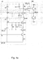
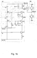
- Fig. 1 shows a first level shifter according to the invention in two embodiments.
- Fig. 2 shows simulation results of a level shifter according to Fig. 1 a.
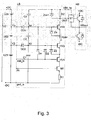
- Fig. 3 shows a second embodiment of a Levelshifters invention.
- Fig. 4 shows comparative simulations of the level shifter according to Fig. 1a and Fig. 3 ,
- Fig. 5 shows a third inventive design of a Levelshifters.
- Fig. 6 shows a fourth inventive design of a Levelshifters.
- Fig. 1a shows an arrangement with a level shifter (LS) according to the invention, wherein a switching transistor (M1) and a number n of high-voltage transistors (HV1 to HVn) are connected in series. All transistors are in a signal transmission from the low side to the high side of the n-channel type.
- a first resistor (R1) is connected to the source of the switching transistor (M1), and to the ground line (gnd_Is) of the low side.
- a second resistor (R2) is connected to the drain of the last high voltage transistor (HVn) and to the high side (vdd_hs) operating voltage terminal.
- the input of the level shifter, to which the signal to be transmitted is transferred, is connected directly to the gate of the switching transistor (M1).
- the drain terminal of the last high voltage transistor (HVn) is the output (OUT) of the level shifter (LS).
- a signal evaluation circuit (ST), for example a Schmitt trigger, is connected to this.
- the ground line of the signal evaluation circuit (ST) is connected to the Central node (HBout) of a power half-bridge (HB) connected.
- the central node (HBout) of the half-bridge (HB) forms the reference potential (gnd_hs) of the high side and is depending on the switching state of the power semiconductors (TOP, BQT) either close to the intermediate circuit voltage (UZ) at the positive electrode (+ DC) of the DC link or near the potential at the negative electrode (-DC) of the intermediate circuit, which is usually connected to the ground line (gnd_ls).
- the operating voltage supply for the circuits on the high side can be realized with known techniques. These include the bootstrap power supply or DC / DC converters.
- the gate of the first high-voltage transistor (HV1) is connected directly to the operating voltage line (vdd_Is) of the low side and thus always receives a constant potential, for example 15V, which is generated by a DC voltage source.
- vdd_Is operating voltage line
- vdd_l potential
- vdd_l potential
- the first diodes (D2 to Dn) are forward-biased and connected to the gate Terminals of the associated high-voltage transistors (HV2 to HVn) is at a defined potential, which corresponds almost to the voltage generated by the DC voltage source, minus the diode forward voltages.
- On the gate at the control input (IN) of the switching transistor (M1) is a prepared by the drive logic of the gate driver periodically occurring control signal, for example, a rectangular pulse given.
- the control signal causes switching of the switching transistor (M1).
- the high voltage transistors (HV1 to HVn) are turned on and off.
- a cross-flow (lquer) flows through the level shifter (LS).
- the digital input signal is thus converted into a current signal and transmitted via the level shifter (LS).
- the voltage drop across the second resistor (R2) is proportional to the cross current (Iquer).
- the signal evaluation circuit (ST) connected to the output (OUT) of the level shifter (LS) converts the transmitted signal back into a digital signal.
- the level shifter invention requires in contrast to the training after In the prior art no further signal transmission circuits to n-1 intermediate potentials.
- a signal transmitted to the high side leads to a switching operation of the TOP switch of the power half-bridge (HB).
- HB power half-bridge
- the voltage at the output of the half-bridge (HBout) increases with a rapid change per unit time (du / dt), exemplarily 10kV / ⁇ s.
- the reference potential of the high side increases at the same time.
- the varying voltage divides evenly across the node (X2 to Xn), so that across each capacitor a voltage drops, the n-th part of the currently applied voltage between (vdd_hs) and (gnd_Is) matches.
- the maximum voltage which can drop across a capacitor (C1 to Cn) corresponds approximately to the nth part of the intermediate circuit voltage (UZ).
- the voltage division produced by the capacitors remains even after the decay of the voltage change over time, since the capacitors (C1 to Cn) hold the stored charge.
- the first diodes (D2 to Dn) are reverse-biased. These diodes (D2 to Dn) require a breakdown voltage which is at least as great as the maximum occurring voltage between the nodes (X2 to Xn) and (vdd_Is).
- each high-voltage transistor HV2 to HVn
- a Zener diode Z2 to Zn
- the gate-source voltage of each high voltage transistor thereby becomes low limited above a value which is below the breakdown voltage of the gate-source path of a high voltage transistor and thus prevents a breakdown of the device.
- the zener voltage of the Zener diode typically only a few volts, may be neglected for consideration of the intermediate potential adjustment versus the intermediate circuit voltage.
- the potential at the gate of a high voltage transistor is based on the source of the same transistor or on the drain of the underlying transistor.
- About the drain-source path of each high-voltage transistor (HV1 to HVn) can thus fall about only a maximum of the nth part of the intermediate circuit voltage (UZ).
- UZ intermediate circuit voltage
- LS level shifter
- Another zener diode (Zn + 1) is connected in parallel with the second resistor (R2).
- the cathode of (Zn + 1) is connected to (vdd_hs) the anode to the output of the level shifter (LS).
- the voltage drop across (R2) which occurs in a cross-flow through the level shifter, limited such that the potential at the output (OUT) of the level shifter does not fall below the ground potential (gnd_hs) of the downstream Schmitt trigger (ST) and simultaneously Guaranteed voltage swing at the output, which allows a distinction between transmitted high and low levels.
- a preferred value is the magnitude of the operating voltage of the high side, e.g. 15V.
- FIG. 1 b of the level shifter dispenses with the switching transistor (M1) and connects the input (IN) directly to the gate of the first high voltage transistor (HV1 ').
- the first diodes (D2 to Dh) are not connected to the gate of the first high voltage transistor (HV1 ').
- the further embodiment is identical to those according to Fig. 1 a.
- the waiver of the switching transistor (M1, according to Fig. 1 a) However, as a result, the transmission speed is lower for the same switching capacity.
- Fig. 2 is the transient transfer behavior of the level shifter according to Fig. 1 a shown in a simulation.
- the Schmitt trigger correctly recognizes the transmitted signal.
- Fig. 3 shows a second opposite Fig. 1a extended, embodiment of the Levelshifiters (LS) according to the invention.
- An intermediate circuit voltage (UZ) is generated from n similar voltage sources (UZ1 to UZn) which are connected in series with each other, wherein each voltage source can generate the same partial voltage UZ / n.
- the potential at the further node (Y2) thus corresponds to the potential which is to occur maximally at the node (X2).
- the statement applies to the nodes (Y3 and X3 to Yn and Xn). This will be explained further by a simple example.
- the DC link voltage of the system is 600V by way of example.
- the breakdown voltage of the available high-voltage transistors is at least 300V but less than 600V.
- the embodiment is after Fig. 3 supplemented by the further diodes (DD2 to DDn).
- the anodes of these diodes are respectively connected to the nodes (X2 to Xn), the corresponding cathodes to the other nodes (Y2 to Yn).
- the signal transmission via the level shifter (LS) is analogous to the first embodiment.
- the setting of the potentials at the nodes (X2 to Xn) in a switching operation in which the BOT switch on and the TOP switch is turned off, is further achieved by the capacitors (C1 to Cn).
- the maximum potential at the nodes (X2 to Xn) is thereby limited to the constant potential at the corresponding further node (Y2 to Yn) upwards.
- the drain-source voltage of (HV1 and HV2) is not greater than a maximum of 300V, so that the breakdown voltage of the transistors is not exceeded. If the capacitance of (C1) is greater than (C2), then over (C2) most of the currently applied voltage drops between (vdd_hs and gnd_Is). Thus, the drain-to-source voltage of (HV2) may exceed the breakdown voltage, that is, the desired withstand voltage of the level shifter (LS) may not be ensured. Thus, the case where the capacitance of (C2) is greater than (C1) represents the preferred variant, since the voltage limitation at the gate of (HV2) always becomes effective and the breakdown voltage of (HV2) can not be exceeded.
- the capacitances of (C1 to Cn) are dimensioned such that the capacitances of the respective capacitors (C1 to Cn) increase with their ordinal number (1 to n).
- This advantageous embodiment of the level shifter (LS) is therefore suitable for applications in which the values of the capacitors (C1 to Cn) scatter strongly or certain parasitic capacitances of the arrangement can not be calculated precisely or are subject to changes as a result of the application.
- Fig. 5 represents a further embodiment of the Levelshifters (LS) according to the invention, with which it is possible to transmit signals via a potential barrier, which is greater than the dielectric strength between high side and low side in an integrated circuit.
- This dielectric strength is determined, on the one hand, by the breakdown voltage of the integrated level shifter, which is determined by the breakdown voltage of the integrated high-voltage transistor in conventional topologies, and on the other hand by the dielectric strength of the insulation between high side and low side.
- the dielectric strength of the insulation is determined by semiconductor technology and can not be increased with circuit measures.
- the dielectric strength of the level shifter as described above, by the use of n high-voltage transistors in an HVIC on the n-fold value, that is at the maximum on the dielectric strength of the Isolation can be increased.
- the withstand voltage of the entire level shifter can only be increased to n times the value if each of the n high voltage transistors is integrated on a separate substrate.
- higher potential differences can be overcome with prior art 600V isolation techniques. For example, if two chips are used, an integrated circuit arrangement can also be realized for the voltage class of 1200V.
- the embodiment in Fig. 5 differs from the one according to Fig. 3 in that the level shifter is subdivided into n separate chips (Ch1 is Chn), one of the n high-voltage transistors (HV1 to HVn) being integrated on each chip.
- Ch1 is Chn
- HV1 to HVn high-voltage transistors
- On chip (Ch1) the high voltage transistor (HV1), the switching transistor (M1) and the first resistor (R1) are integrated.
- on chip (Ch1) further circuits such as a logic board and a driver for a BOT switch can be integrated.
- the chips (Ch2 to Chn-1) each contain a high-voltage transistor (HV2 to HVn-1) and the associated Zener diodes (Z2 to Zn-1), as in the aforementioned embodiments to the high voltage transistors (HV2 to HVn -1) are connected.
- the first and second diodes (D2 to Dn and DD2 to DDn) can be integrated on the respective chip (Ch2 to Chn) if the maximum occurring reverse voltage at the diode is less than the dielectric strength of the insulation of the chip. If the maximum occurring blocking voltage at the diodes (D2 to Dn and DD2 to DDn) is greater than the dielectric strength of the insulation of the chip, then the corresponding diodes must be designed as external components.
- the chip (Chn) contains the high voltage transistor (HVn), the zener diodes (Zn, Zn + 1) and the resistor (R2).
- HVn high voltage transistor
- Zn, Zn + 1 the zener diodes
- R2 the resistor
- all other circuit parts of the high side e.g. the signal evaluation circuit and the driver for the TOP switch are integrated.
- the capacitors (C1 to Cn) can be integrated in the associated chips (Ch1 to Chn). Due to the high chip area required for the capacitors, the implementation with external discrete components is a preferred embodiment.
- this level shifter without the voltage-limiting diodes (DD2 to DDn) is analogous to the first embodiments Fig. 1a and b possible.
- each chip Ch1 to Chn
- a change in the potential at the backside contact of a chip alters the electrical behavior of the devices at the top. This effect is known as the back channel effect.
- the backside contact In pn isolated prior art technologies, the backside contact must always carry the lowest potential occurring in the chip, otherwise the back pn junction, which is to receive the voltage between high side and low side, is poled in the forward direction and thus does not fulfill the function can.
- the backside contact (HW) is dielectrically isolated from the devices on top of the wafer, so isolation is not compromised even with a higher back contact potential. A noticeable influence of the increased backside potential on the electrical behavior of the components typically only starts at a few 10V.
- This advantage of the SOI technology is used in the inventive circuit in this.
- the backside contacts (HW2 to HWn) of the chips (Ch2 to Chn) are respectively connected to the gate terminals of the corresponding high voltage transistors (HV2 to HVn) and to the corresponding nodes (X2 to Xn).
- the potential at the source terminal of a high voltage transistor is always the lowest potential that occurs in the chip in which the high voltage transistor has been integrated.
- the Zener diodes (Z2 to Zn) limit the gate-to-source voltage of the transistors (HV2 to HVn) to a few volts, 15V by way of example, and maintain the potential at the source of the integrated high voltage transistor close to the potential of the backside contact of the respective chip.
- the chips (Ch1 to Chn) are mutually insulated, but advantageously arranged in a common package. The electrical connection between the chips can be achieved by known methods, for example a bonding method.
- FIG. 6 shows a level shifter in a fourth embodiment.
- the variant presented here is a level shifter, which transmits a voltage signal, which was generated on the high side, to the low side in order to be evaluated there by a logic circuit.
- the signal can be passed from the low side to a microcontroller.
- the voltage signal can be, for example, a status signal of a monitoring circuit (US) which detects the operating state of certain subcircuits of the high side, for example a monitoring of the operating voltage or the temperature of a subcircuit.
- the microcontroller can thus monitor the status signal an operating state on the high side.
- US monitoring circuit
- the level shifter (LS) is complementary to the embodiment according to FIG 1a built up. That is, the same topology is used, with the difference that both the n high-voltage transistors (HV1 to HVn) and the switching transistor (M1) are of the p-channel type.
- the first resistor (R1), the transistors (M1, HV1 to HVn) and the second resistor (R2) are in turn connected in series.
- One terminal of the first resistor (R1) is connected to the source of the switching transistor (M1), the other terminal to the operating voltage line (vdd_hs) of the high side.
- the second resistor (R2) is connected to the drain of the transistor (HVn) and to the ground line (gnd_ls) of the low side.
- the gate terminal of the switching transistor (M1) is the input (IN) of the level shifter (LS), to which the signal to be transmitted is transferred.
- the drain terminal of the high voltage transistor (HVn) is the output (OUT) of the level shifter.
- a signal evaluation circuit eg a Schmitt trigger, is connected.
- the mass of the signal evaluation circuit is connected to the ground line (gnd_ls) of the low side.
- the anode of one of the first diodes (D2 to Dn) is connected to the gate terminals of the Hocbspanpungstransistoren (HV2 to HVn) in each case.
- the cathodes of the diodes are connected to the potential (gnd_hs).
- the diodes (D2 to Dn) are forward-biased and connected to the gate terminals of the high-voltage transistors (HV2 to HVn) there is a defined potential which corresponds almost to the potential of (gnd_hs).
- a zener diode (Zn + 1) is connected in parallel with the second resistor (R2).
- the anode of (Zn + 1) is connected to (gnd_Is), the cathode to the output (OUT) of the level shifter (LS).
- (Zn + 1) limits the voltage drop across (R2) as in the first embodiment in FIG Fig. 1 described.
- the capacitive voltage divider between (vdd_hs) and (gnd_ls), consisting of the capacitors (C1 to Cn), which are connected in series with one another, is connected as in the first embodiment and takes over the adjustment of the potential at the gate electrodes of the high-voltage transistors ( HV2 to HVn) at a time change of the reference potential of the high side in the manner described.
- a Zener diode (Z2 to Zn) is connected to each high-voltage transistor (HV2 to HVn), the cathode being connected to the source and the anode to the gate of the high-voltage transistor.
- the gate-source voltage of each high-voltage transistor (HV2 to HVn) is thereby limited, thus preventing the breakdown of the device.
- the signal transmission of a voltage signal from the high side to the low side is analogous to the signal transmission from the low side to the high side in the first embodiment.
- the control signal is applied to the gate of the switching transistor (M1) and causes switching of the switching transistor (M1).
- the high voltage transistors (HV1 to HVn) are turned on and off.
- a cross current (Iquer) flows through the level shifter (LS).
- the digital input signal is converted into a current signal and transmitted via the level shifter.
- the voltage drop across the second resistor (R2) is proportional to the cross current.
- the signal evaluation circuit (ST) connected to the output (OUT) of the level shifter (LS) converts the transmitted signal into a digital signal.
Landscapes
- Engineering & Computer Science (AREA)
- Computer Hardware Design (AREA)
- Physics & Mathematics (AREA)
- Computing Systems (AREA)
- General Engineering & Computer Science (AREA)
- Mathematical Physics (AREA)
- Logic Circuits (AREA)
- Electronic Switches (AREA)
- Power Conversion In General (AREA)
- Dc-Dc Converters (AREA)
Description
- Die Erfindung beschreibt einen Levelshifter vorzugsweise für einer Ansteuerschaltung die in leistungselektronischen Systemen benötigt wird um Leistungshalbleiterschalter anzusteuern, die als Einzeischalter oder in einer Brückenschaltung angeordnet sind. Derartige Brückenschaltungen sind als Ein-, Zwei-, oder Dreiphasen-Brückenschaltungen bekannt, wobei die einphasige sog. Halbbrücke einen Grundbaustein leistungselektronischer Schaltungen darstellt. In einer Halbbrückenschaltung sind zwei Leistungsschalter, ein erster sog. TOP-Schalter und ein zweiter sog. BOT-Schalter in einer Reihenschaltung angeordnet.
- Eine derartige Halbbrücke weist in der Regel eine Verbindung zu einem Gleichstromzwischenkreis auf. Der Ausgang, typischerweise der Wechselspannungsanschluss der Halbbrücke ist meist mit einer Last verbunden. Die Ansteuerschaltung besteht in der Regel aus mehreren Teilschaltungen bzw. Funktionsblöcken. Das Steuersignal wird in einer ersten Teilschaltung, der Ansteuerlogik, aufbereitet und über weitere Komponenten den Treiberschaltungen und schließlich dem Steuereingang des jeweiligen Leistungsschalters zugeführt.
- Bei höheren Zwischenkreisspannungen, beispielhaft größer 100V, wird meist die Ansteuerlogik potentialmäßig von den Treiberschaltungen getrennt, da sich die zugehörigen Leistungsschalter auf unterschiedlichem Potential befinden und somit eine spannungsmäßige Isolation unumgänglich ist. Diese Trennung gilt zumindest für den TOP-Schalter, wird aber bei höheren Leistungen auch für den BOT-Schalter auf Grund eines möglichen Verrisses des Massepotentials beim Schalten ausgeführt. Eine derartige Trennung kann zum Beispiel durch Impulsübertrager (galvanische Trennung), durch Optokoppler bzw. Lichtwellenleiter oder mit Hilfe integrierter Schaltungstechnik in einem HVIC (High Voltage Integrated Circuit) realisiert werden. Letztere Variante wird, aufgrund verschiedener Vorteile, wie geringe Abmessungen, niedriger Preis und lange Lebensdauer, mit zunehmender Häufigkeit eingesetzt. Gleichzeitig bieten HVICs die Möglichkeit, ein Hochspannungsbauelement, mit einer Durchbruchspannung größer oder gleich der Zwischenkreisspannung zu integrieren, welche in Schaltkreisen zur Signalpegelumsetzung, in sogenannten Levelshiftern, eingesetzt werden kann. Üblicherweise wird für diese ein lateraler Hochspannungs- MOSFET verwendet.
- Der vorgestellte Schaltungsteil ist Teil der Ansteuerschaltung und vorzugsweise ausgeführt als eine integrierte Schaltungsanordnung. Er dient der Übertragung eines Signals von einem Schaltungsteil mit einem niedrigen Bezugspotential (low side) zu einem Schaltungsteil mit einem zeitweise höheren Bezugspotential (high side) oder umgekehrt. Eine solche Anordnung wird zur integrierten und potentialgetrennten Ansteuerung von Leistungshalbleitern benötigt und als Levelshifter bezeichnet.
- Es sind zwei grundsätzliche lsolationstechnologien bei HVICs bekannt. Einerseits die SOI-(Silicon on Insulator) Technologien und andererseits pn- isolierte Technologien (Junction Isolation). Die SOI-Technologie bietet eine dielektrische Isolation von Bauelementen und Bauelementgruppen, steht aber derzeit nur bis 800V Spannungsfestigkeit zur Verfügung. Die SOI- Substratwafer sind deutlich teurer als Standardsubstrate, allerdings werden die Kosten durch erhebliche Prozessvereinfachungen kompensiert, die sich aus der dielektrischen Isolation ergeben. Bei pn- isolierten Technologien wird die Sperrspannung durch einen sperrgepolten pn-Übergang aufgenommen. Diese Technik steht derzeit bis 1200V zur Verfügung. Die Herstellung ist allerdings sehr aufwendig und somit kostenintensiv. Weiterhin gibt es technische Probleme, beispielhaft mit Leckströmen und Latch- up Effekten u.a. bei höheren Temperaturen, wie beispielhaft mehr als 125°C Betriebstemperatur, sowie bei Verriss des Massepotentials bei schnellen dynamischen Vorgängen.
- Wie in der
DE10152930A1 offenbart, lässt sich ein Signal auch schrittweise mittels einer Mehrzahn n gleichartiger kaskadiert, geschalteter bekannter Levelshifter umsetzen, wobei n hier und im Folgenden eine ganze Zahl von zwei oder mehr ist. Die Durchbruchspannung eines einzelnen Hochspannungsbauelements als Teil des Levelshifters muss damit nur den n- ten Teil der Gesamtspannung betragen (Zwischenkreisspannung plus die maximale dynamische Überspannung beim Schalten), vorausgesetzt die gesamte Spannung verteilt sich gleichmäßig auf alle n Levelshifter. Ebenso kann der nutzbare Pegelverschiebungsbereich vergrößert werden, wenn die Anzahl der Stufen erhöht wird. Jedem einzelnen Levelshifter kann eine Signalübertragungsschaltung nachgeschaltet werden. Aus einem resistiv arbeitenden Spannungsteilerschaltkreis, der an das wechselnde Potential am Ausgang der Leistungshalbbrücke gekoppelt ist, werden die Zwischenpotentiale für die negativen Anschlüsse der Versorgungsspannung für den ersten bis (n-1)- ten Signalübertragungsschaltkreis abgeleitet. - Da sich das Potential am Ausgang zyklisch zwischen 0V und einer vorgegebenen Spannung, beispielsweise 600V, ändert, wechselt der Abstand zwischen jeweils zwei Zwischenpotentialen in einem Bereich von beinahe 0V bis 600V/n. Durch diese, an die Schaltphasen der Leistungshalbbrücke gebundene, gleichmäßige Erzeugung von Zwischenpotentialen wird dafür gesorgt, dass die Durchbruchspannung des Hochspannungsbauelements in keinem der n Levelshifter überschritten werden kann.
- Die in der
DE10152930A1 offenbarte Kaskadierung von n Levelshiftern hat allerdings den Nachteil, dass sich die Anzahl der Querstrompfade, mit einem Querstrompfad pro Levelshifter, um das n- fache, gegenüber einem einzelnen Levelshifter, erhöht. Somit steigt die Stromaufnahme und damit auch die Verlustleistung der Levelshifteranordnung um den Faktor n an. Durch einen Spannungsteilerschaltkreis, der die n-1 Zwischenpotentiale für die Levelshifter erzeugt, fließt zusätzlich ein statischer Querstrom der die Verlustleistung weiter erhöht. - Die Spannungsversorgung für jeden der Signalübertragungsschaltkreise erfolgt über eine Bootstrap- Spannungsversorgung nach dem Stand der Technik, das heißt dass jeweils ein Kondensator an den Betriebsspannungs- und Masseanschluss des Signalübertragungsschaltkreises angeschlossen ist und zyklisch, entsprechend der Schaltphase der Halbbrücke, von einer Gleichstromquelle aufgeladen wird. Da Signalübertragungsschaltkreis separat versorgt wird steigt der Schaltungs- und Platzaufwand für die Versorgung auf den n- fachen Wert an.
- Weiterhin sind aus der
DE10152930A1 verschiedene Ausführungsformen zur Signalpegelumsetzung in mehreren Stufen bekannt. So kann beispielhaft ein Signal, das aus einem Messkreis zur Erfassung eines Betriebszustandes des TOP-Schalters auf der high side gewonnen wird, über mehrere Levelshifter an eine low side-Signalverarbeitungsschaltung übertragen und einem Mikrocontroller zugeführt werden. Als Hochspannungsbauelement für einen entsprechenden Levelshifter kann ein p-Kanal Hochspannungs- MOSFET genutzt werden. Der Mikrocontroller kann durch dieses Erfassungssignal den Betriebszustand des TOP-Schalters überwachen. Auch für diese Variante gelten die beschriebenen Nachteile in gleicher Weise. - Die Druckschrift von M. VANDER KOOI ET AL "MOS moves into higher- power applications" (ELECTRONICS, Bd. 49, Nr. 13, 24.Juni 1976, Seiten 98 - 103, XP002531713) offenbart ein Power MOSFET integriert in eine Spannungsteilerschaltung, eine Reihenschaltung von Hochspannungstransistoren mit parallel geschalteten Kondensatoren mit einem dazwischen geschalteten Knotenpunkt der mit einem Transistor verbunden ist aufweist und ein Ausgangspannung regelt zwischen den Bezugspotentialen von + 15 V und + 100 V.
- Die Druckschrift von B. SERNEELS ET AL: "7.8 - A High Voltage Output Driver in a Standard 2.5 0.25/spl mu/m CMOS Technology" (15. Februar 2004, IEEE INTERNATIONAL SOLID-STATE CIRCUITS CONFERENCE 2004; DIGEST OF TECHNICAL PAPERS. IEEE, PISCATAWAY, NJ, USA, Pages 146 - 155, XP010722195; ISBN: 978-0-7803-8267-1) offenbart ein Hochspannungsausgangstreiber der CMOS Technology, der ebenfalls eine Reihenschaltung von Hochspannungstransistoren mit parallel geschalteter Reihenschaltung von Kondensatoren, die einen Knoten aufweisen die mit dem Steuereingang eines Hochspannungstransistors verbunden ist.
- Der Erfindung liegt die Aufgabe zugrunde einen Levelshifter beispielhaft für Ansteuerschaltunhen von Leistungshalbleiterbauelementen vorzugsweise in form mindestens einer integrierten Schaltung derart weiterzubilden, dass der Leistungsverbrauch und der Schaltungsaufwand im Vergleich zum Stand der Technik reduziert sind.
- Die Aufgabe wird erfindungsgemäß gelöst durch die Maßnahmen der Merkmale des Anspruchs 1 Bevorzugte Ausführungsformen sind in den Unteransprüchen beschrieben.
- Der erfinderische Gedanke geht aus von einer Ansteuerschaltung mit einem Levelshifter zur unidirektionalen Übertragung eines Signals von einem ersten Schaltungsteil mit erstem Potential zu einem zweiten Schaltungsteil mit zweitem Potential. Hierzu weist die Ansteuerschaltung einen Levelshifter, ausgeführt als eine Reihenschaltung einer Mehrzahl von Transistoren auf, wobei der Eingang des Levelshifters mit dem Steuereingang des ersten Transistors der Reihenschaltung verbunden ist. Dieser erste Transistor ist ein Schalttransistor oder ein Hochspannungstransistor während alle weiteren Transistoren Hochspannungstransistoren sind.
- Weiterhin weist der Levelshifter einen kapazitiven Spannungsteilerschaltung parallel geschaltet zu den Hochspannungstransistoren auf, wobei dieser kapazitive Spannungsteiler zwischen einem Bezugspotential der low side und einem Bezugspotential der high side geschaltet ist Ebenso weist der Levelshifter Knoten zwischen den einzelnen Kondensatoren auf, die mit den Steueranschlüssen der zugeordneten Hochspannungstransistoren verbunden sind.
- Vorteilhaft an der erfindungsgemäßen Topologie ist, dass sich durch die Verwendung von n Hochspannungstransistoren die n- fache Sperrfähigkeit eines einzelnen Hochspannungstransistors erreichen lässt. Gleichzeitig weist die erfindungsgemäße Schaltung, gegenüber der beschriebenen Schaltung nach dem Stand der Technik lediglich einen und nicht n Querstrompfade auf: Weiterhin enthält die erfindungsgemäße Schaltung keine Signatverärbeitungsschaltungen auf Zwischenpotentialen, so dass auch keine aufwendige Stromversorgung dieser Schaltkreise benötigt wird.
- Somit kann zum einen der Leistungsverbrauch und zum anderen der Schaltungsaufwand gegenüber dem Stand der Technik verringert werden. Dies hat einen geringeren Platz-und somit auch einen geringeren Kostenbedarf zur Folge.
- Besonders bevorzugte Ausbildungen des Levelshifters sind in der jeweiligen Beschreibung der Ausführungsbeispiele genannt. Die erfinderische Lösung wird zudem an Hand dieser Ausführungsbeispiele der
Fig. 1 bis 6 weiter erläutert. -
Fig. 1 zeigt einen ersten erfindungsgemäßen Levelshifter in zwei Ausführungsformen. -
Fig. 2 zeigt Simulationenergebnisse eines Levelshifters gemäßFig. 1 a. -
Fig. 3 zeigt eine zweite Ausgestaltung eines erfindungsgemäßen Levelshifters. -
Fig. 4 zeigt vergleichende Simulationen der Levelshifter gemäßFig. 1a undFig. 3 . -
Fig. 5 zeigt eine dritte erfindungsgemäße Ausbildung eines Levelshifters. -
Fig. 6 zeigt eine vierte erfindungsgemäße Ausbildung eines Levelshifters. -
Fig. 1a zeigt eine Anordnung mit einem erfindungsgemäßen Levelshifters (LS), wobei ein Schalttransistor (M1) und eine Anzahl n Hochspannungstransistoren (HV1 bis HVn) in Reihe geschaltet werden. Alle Transistoren sind bei einer Signalübertragung von der low side zur high side vom n-Kanal Typ. Ein erster Widerstand (R1) wird an Source des Schalttransistors (M1), und an die Masseleitung (gnd_Is) der low side angeschlossen. Ein zweiter Widerstand (R2) wird an Drain des letzten Hochspannungstransistors (HVn) und an den Betriebsspannungsanschluss der high side (vdd_hs) angeschlossen. Der Eingang des Levelshifters, an den das zu übertragende Signal übergeben wird, ist direkt mit dem Gate des Schalttransistors (M1) verbunden. Der Drain- Anschluss des letzten Hochspannungstransistors (HVn) ist der Ausgang (OUT) des Levelshifters (LS). An diesen wird eine Signalauswerteschaltung (ST), beispielhaft ein Schmitt- Trigger angeschlossen. Die Masseleitung der Signalauswerteschaltung (ST) ist an den Mittelknoten (HBout) einer Leistungshalbbrücke (HB) angeschlossen. Der Mittelknoten (HBout) der Halbbrücke (HB) bildet das Bezugspotential (gnd_hs) der high side und befindet sich je nach Schaltzustand der Leistungshalbleiter (TOP, BQT) entweder nahe der Zwischenkreisspannung (UZ) an der positiven Elektrode (+DC) des Zwischenkreises oder nahe dem Potential an der negativen Elektrode (-DC) des Zwischenkreises, die üblicherweise mit der Masseleitung (gnd_ls) verbunden ist. - Die Betriebsspannungsversorgung für die Schaltkreise auf der high side kann mit bekannten Techniken realisiert werden. Dazu gehören unter anderem die Bootstrap-Spannungsversorgung oder DC/DC-Wandler.
- Das Gate des ersten Hochspannungstransistors (HV1) wird direkt an die Betriebsspannungsleitung (vdd_Is) der low side angeschlossen und erhält somit immer ein gleich bleibendes Potential, beispielhaft 15V, das von einer Gleichspannungsquelle erzeugt wird. An die Gate- Anschlüsse der weiteren Hochspannungstransistoren (HV2 bis HVn) ist jeweils die Kathode einer zugeordneten ersten Diode (D2 bis Dn), wobei diese Dioden auch als Reihenschaltung einer Mehrzahl von Dioden ausgestaltet sein können, angeschlossen. Die Anoden der ersten Dioden (D2 bis Dn) sind an das Potential (vdd_ls) angeschlossen. Bei einem Schaltzustand bei dem das Bezugspotential von high side und low side gleich ist, das heißt der Wert von (gnd_hs) ist gleich dem Wert von (gnd_Is), sind die ersten Dioden (D2 bis Dn) in Durchlassrichtung gepolt und an den Gate- Anschlüssen der zugeordneten Hochspannungstransistoren (HV2 bis HVn) liegt ein definiertes Potential an, welches nahezu der Spannung entspricht, die von der Gleichspannungsquelle erzeugt wird, abzüglich der Dioden- Flussspannungen.
- Auf das Gate am Steuereingang (IN) des Schalttransistors (M1) wird ein von der Ansteuerlogik des Gatetreibers aufbereitetes periodisch auftretendes Steuersignal, beispielhaft ein rechteckförmiger Impuls, gegeben. Das Steuersignal bewirkt ein Schalten des Schalttransistors (M1). Dadurch werden die Hochspannungstransistoren (HV1 bis HVn) ein- und ausgeschaltet. Beim Einschalten fließt ein Querstrom (lquer) durch den Levelshifter (LS). Das digitale Eingangssignal wird somit in ein Stromsignal gewandelt und so über den Levelshifter (LS) übertragen. Der.Spannungsabfall über dem zweiten Widerstand (R2) ist proportional zum Querstrom (Iquer).
- Die an den Ausgang (OUT) des Levelshifters (LS) angeschlossene Signalauswerteschaltung (ST) wandelt das übertragene Signal in ein digitales Signal zurück. Der erfindungsgemäße Levelshifter benötigt im Gegensatz zur Ausbildung nach dem Stand der Technik keine weiteren Signalübertragungsschaltungen auf n-1 Zwischenpotentialen.
- Anschließend wird das Signal einer weiteren logischen Signalverarbeitung unterzogen oder direkt an den Treiber für den TOP-Schalter übergeben. Ein auf die high side übertragenes Signal führt zu einem Schaltvorgang des TOP-Schalters der Leistungshalbbrücke (HB). Bei einem Schaltvorgang der Leistungshalbbrücke (HB), bei der gleichzeitig oder kurz nacheinander der BOT-Schalter aus und der TOP-Schalter eingeschaltet werden, steigt die Spannung am Ausgang der Halbbrücke (HBout) mit einer schnellen Änderung pro Zeiteinheit (du/dt), beispielhaft 10kV/µs an. In gleichem Maße steigt gleichzeitig das Bezugspotential der high side an. Nach dem Schaltvorgang liegt zwischen den Potentialen (vdd_hs und vdd_ls bzw. zwischen gnd_hs und gnd_ls) etwa die Zwischenkreisspannung (UZ) an. Der größte Teil der Spannung fällt über den Hochspanhungstransistoren (HV1 bis HVn) ab.
- Ein kapazitiver Spannungsteiler zwischen (vdd_hs) und (gnd_Is), bestehend aus Kondensatoren (C1 bis Cn), die untereinander in Reihe geschaltet sind, erzeugt bei einer zeitlichen Änderung der Ausgangsspannung der Halbbrücke (HB) n-1 Zwischenpotentiale an den Knoten (X2 bis Xn), die jeweils an die Gates der Hochspannungstransistoren (HV2 bis HVn) angeschlossen sind. Bei geeigneter Dimensionierung der Kondensatoren (C2 bis Cn) teilt sich die ändernde Spannung gleichmäßig über den Knoten (X2 bis Xn) auf, so dass über jedem Kondensator eine Spannung abfällt, die dem n-ten Teil der gerade anliegenden Spannung zwischen (vdd_hs) und (gnd_Is) entspricht.
- Die maximale Spannung die über einem Kondensator (C1 bis Cn) abfallen kann entspricht etwa dem n- ten Teil der Zwischenkreisspannung (UZ). Die durch die Kondensatoren erzeugte Teilung der Spannung bleibt auch nach dem Abklingen der zeitlichen Spannungsänderung erhalten, da die Kondensatoren (C1 bis Cn) die gespeicherte Ladung halten. Wenn das Bezugspotential der high side höher ist als das Bezugspotential der low side dann sind die ersten Dioden (D2 bis Dn) in Sperrrichtung gepolt. Diese Dioden (D2 bis Dn) benötigen eine Durchbruchspannung die mindestens so groß ist wie die maximal auftretende Spannung zwischen den Knoten (X2 bis Xn) und (vdd_Is).
- An jedem Hochspannungstransistor (HV2 bis HVn) ist weiterhin jeweils eine Zener-Diode (Z2 bis Zn) angeschlossen, wobei die Kathode am Gate und die Anode am Source des zugeordneten Hochspannungstransistors angeschlossen ist. Die Gate-Source-Spannung jedes Hochspannungstransistors (HV2 bis HVn) wird dadurch nach oben auf einen Wert begrenzt der unterhalb der Durchbruchspannung der Gate-Source-Strecke eines Hochspannungstransistors liegt und verhindert somit einen Durchbruch des Bauelements. Die Zener-Spannung der Zener-Diode, typischerweise nur einige Volt, kann für die Betrachtung der Zwischenpotentialeinstellung gegenüber der Zwischehkreisspannung vernachlässigt werden.
- Somit ist das Potential am Gate eines Hochspannungstransistors auf Source des gleichen Transistors bzw. auf Drain des darunter liegender Transistors bezogen. Über der Drain-Source-Strecke eines jeden Hochspannungstransistors (HV1 bis HVn) kann somit etwa nur maximal der n- te Teil der Zwischenkreisspannung (UZ) abfallen. Somit lässt sich eine Spannungsfestigkeit des gesamten Levelshifters (LS) erreichen, die etwa dem n- fachen der Durchbruchspannung der Drain-Source-Strecke eines Hochspannungstransistors entspricht.
- Eine weitere Zener-Diode (Zn+1) ist parallel zum zweiten Widerstand (R2) geschaltet. Die Kathode von (Zn+1) ist an (vdd_hs) die Anode an den Ausgang des Levelshifters (LS) angeschlossen. Dadurch wird der Spannungsabfall über (R2), der bei einem Querstrom durch den Levelshifter auftritt, derart begrenzt, dass das Potential am Ausgang (OUT) des Levelshifters das Massepotential (gnd_hs) des nach geschalteten Schmitt- Triggers (ST) nicht unterschreitet und gleichzeitig einen Spannungshub am Ausgang garantiert, der eine Unterscheidung zwischen übertragenem high- und low-Pegel ermöglicht. Ein bevorzugter Wert ist die Höhe der Betriebsspannung der high side, z.B. 15V. Durch die Einstellung der Zwischenpotentiale an den Gates der Hochspannungstransistoren (HV2 bis HVn) mittels des kapazitiven Spannungsteilers ist eine Signalübertragung über den Levelshifter (LS), während aller Betriebszustände der Halbbrücke (HB), möglich.
- Eine weitere vereinfacht Ausgestaltung gemäß
Fig. 1 b des Levelshifters verzichtet auf den Schalttransistor (M1) und verbindet den Eingang (IN) direkt mit dem Gate des ersten Hochspannungstransistors (HV1'). Im Gegensatz zu Ausgestaltung nachFig. 1a sind die ersten Dioden (D2 bis Dh) nicht mit dem Gate des ersten Hochspannungstransistors (HV1') verbunden. Die weitere Ausgestaltung ist identisch derjenigen gemäßFig. 1 a. Der Verzicht auf den Schalttransistor (M1, gemäßFig. 1 a) hat allerdings zur Folge, dass bei gleicher Schaltleistung die Übertragungsgeschwindigkeit geringer ist. - In
Fig. 2 ist das transiente Übertragungsverhalten des Levelshifters gemäßFig. 1 a im Rahmen einer Simulation dargestellt. Hierbei ist eine Ausführungsform mit zwei Hochspannungstransistoren für die Simulation gewählt worden. Aus den Abbildungen ist ersichtlich, dass ein Ansteuersignal (IN) sowohl bei gleichem Bezugspotential von high side und low side (Uoffset=0V) als auch bei einem high side Bezugspotential in der Nähe der Zwischenkreisspannung (Uoffset=600V/1200V) von low side nach high side übertragen wird (OUT). Der Schmitt-Trigger erkennt das übertragene Signal korrekt. Das Potential am Knoten X1 stellt sich bei C1=C2 wie gewünscht auf etwa auf die Hälfte der Zwischenkreisspannung von 600V ein. -
Fig. 3 zeigt eine zweite gegenüberFig. 1a erweiterte, Ausführungsform des erfindungsgemäßen Levelshifiters (LS). Eine Zwischenkreisspannung (UZ) wird aus n gleichartigen Spannungsquellen (UZ1 bis UZn) erzeugt die untereinander in Reihe geschaltet sind, wobei jede Spannungsquelle die gleiche Teilspannung UZ/n erzeugen kann. Das Potential am weiteren Knoten (Y2) entspricht somit dem Potential das maximal am Knoten (X2) auftreten soll. Analog gilt die Aussage für die Knoten (Y3 und X3 bis Yn und Xn). Dies soll an einem einfachen Beispiel weiter erläutert werden. Die Zwischenkreisspannung des Systems beträgt beispielhaft 600V. Die Durchbruchspannung der verfügbaren Hochspannungstransistoren beträgt mindestens 300V ist aber kleiner als 600V. Um die erforderliche Spannungsfestigkeit des Levelshifters zu garantieren müssen also zwei Hochspannungstransistoren in Reihe geschaltet werden, d.h. n=2. Das Potential am Gate von (HV2) wird durch den kapazitiven Spannungsteiler (C1, C2) eingestellt. Wird der Zwischenkreis nun aus zwei Spannungsquellen (UZ1=UZ2) mit jeweils 300V zusammengesetzt, dann entspricht das Potential am Mittelknoten (Y2) des Zwischenkreises genau dem Potential (300V), das am Knoten (X2) (Gate von HV2) anliegen muss um eine annähernd gleichmäßige Spannungsverteilung über den Hochspannungstransistoren (jeweils 300V) zu garantieren. - Zusätzlich zur Anordnung gemäß
Fig.1 wird die Ausführungsform nachFig. 3 um die weitern Dioden (DD2 bis DDn) ergänzt. Die Anoden dieser Dioden werden jeweils an die Knoten (X2 bis Xn), die entsprechenden Kathoden an die weiteren Knoten (Y2 bis Yn) angeschlossen. Die Signalübertragung über den Levelshifter (LS) erfolgt analog zur ersten Ausführungsform. Die Einstellung der Potentiale an den Knoten (X2 bis Xn) bei einem Schaltvorgang bei dem der BOT-Schalter ein- und der TOP-Schalter ausgeschaltet wird, wird weiterhin durch die Kondensatoren (C1 bis Cn) erreicht. Das maximale Potential an den Knoten (X2 bis Xn) wird dabei auf das konstante Potential an den entsprechenden weiteren Knoten (Y2 bis Yn) nach oben begrenzt. Wenn das Potential an einem Knoten (Xk) größer wird als das Potential an einem weiteren Knoten (Yk) zuzüglich der Flussspannung der weiteren Diode (DDk) (2 ≤ k ≤ n) dann öffnet sich die weitere Diode (DDk) und das Potential am Knoten (Xk) kann nicht weiter ansteigen. Zum Einsetzen der Begrenzung kommt es nur, wenn die Kapazität einer oder mehrerer der Kondensatoren (C1 bis Cn) vom gewünschten Wert abweicht bzw. parasitäre Kapazitäten parallel zu einem oder mehreren der Kondensatoren (C1 bis Cn) wirken. Zu einer Abweichung der Kapazität eines Kondensators vom gewünschten Wert kann es beispielsweise durch Parameterstreuung bei der Herstellung kommen. Die Kapazitätsabweichung führt in Folge zu einer unsymmetrischen Spannungsaufteilung. - Durch die Begrenzung der Potentiale an den Knoten (X2 bis Xn) auf einen oberen Wert wird jedoch nicht umfassend sichergestellt, dass die Durchbruchspannung eines Hochspannungstransistors (HV1 bis HVn) nicht überschritten werden kann. Die soll wieder am Beispiel n=2 erläutert werden. Sind C1 und C2 gleich groß, dann stellt sich das Potential am Gate von (HV2) durch den Spannungsteiler etwa auf UZ/2=300V ein und die Begrenzung setzt nicht ein. Ist die Kapazität von (C2) größer als von (C1), dann begrenzt die weitere Diode (DD2) das Potential am Gate von (HV2) (Knoten X2) auf 300V. In beiden Fällen ist auch die Drain-Source-Spannung von (HV1 und HV2) nicht größer als maximal 300V, so dass die Durchbruchspannung der Transistoren nicht überschritten wird. Ist die Kapazität von (C1) größer als von (C2), dann fällt über (C2) der größte Teil der gerade anliegenden Spannung zwischen (vdd_hs und gnd_Is) ab. Somit kann die Drain-Source-Spannung von (HV2) die Durchbruchspannung überschreiten, das heißt die gewünschte Spannungsfestigkeit des Levelshifters (LS) ist gegebenenfalls nicht mehr sichergestellt. Somit stellt der Fall bei dem die Kapazität von (C2) größer ist als von (C1) die bevorzugte Variante dar, da die Spannungsbegrenzung am Gate von (HV2) immer wirksam wird und die Durchbruchspannung von (HV2) nicht überschritten werden kann. Um für die Ausführungsform mit n in Reihe geschalteten Hochspannungstransistoren ein analoges Schaltungsverhalten zu erreichen, werden die Kapazitäten von (C1 bis Cn) so dimensioniert, dass die Kapazitäten der jeweiligen Kondensatoren (C1 bis Cn) mit ihrer Ordnungszahl (1 bis n) steigen. Diese vorteilhafte Ausführungsform des Levelshifters (LS) eignet sich somit für Anwendungen bei denen die Werte der Kondensatoren (C1 bis Cn) stark streuen bzw. bestimmte parasitäre Kapazitäten der Anordnung nicht genau berechenbar sind bzw. durch die Applikation Veränderungen unterliegen.
-
Fig. 4 zeigt das simulierte Verhalten eines Levelshifters für n=2 gemäßFig.1a (linker Teil der Darstellung) und gemäßFig.3 (rechter Teil der Darstellung) während des Einschaltvorganges dar, wobei die Kapazität von (C1) jeweils deutlich kleiner als von (C2) ist. Durch die ungleichmäßige kapazitive Belastung steigt das Zwischenpotential am Knoten (X2) beim Levelshifter nachFig.1a beim schnellen du/dt des high side Bezugspotentials (Vdd_hs) auf einen Wert größer als UZ/2=300V an (ca. 395V). Beim Levelshifter nachFig. 3 steigt das Zwischenpotential am Knoten (X2) nicht über UZ/2, da die beschriebehe Begrenzung durch die weitere Diode (DD2) wirksam wird. -
Fig. 5 stellt eine weitere Ausführungsform des erfindungsgemäßen Levelshifters (LS) dar, mit der es möglich ist Signale über eine Potentialbarriere zu übertragen, die größer ist als die Spannungsfestigkeit zwischen high side und low side in einer integrierten Schaltung. Diese Spannungsfestigkeit wird zum einen bestimmt durch die Durchbruchspannung des integrierten Levelshifters, die bei herkömmlichen Topologien von der Durchbruchspannung des integrierten Hochspannungstransistors bestimmt wird, und zum anderen durch die Spannungsfestigkeit der lsolation zwischen high side und low side. Die Spannungsfestigkeit der lsolation wird von der Halbleitertechnologie bestimmt und kann mit schaltungstechhischen Maßnahmen nicht erhöht werden. Solange die Durchbruchspannung des integrierbaren Hochspannungstransistors mindestens n- mal kleiner ist als die Spannungsfestigkeit der Isolation, kann die Spannungsfestigkeit des Levelshifters, wie oben beschrieben, durch die Verwendung von n Hochspannungstransistoren in einem HVIC auf den n- fachen Wert, also maximal auf die Spannungsfestigkeit der Isolation erhöht werden. - Da in den meisten Fällen die Durchbruchspannung der Isolation und des Hochspannungstransistors annähernd gleich groß sind, kann die Spannungsfestigkeit des gesamten Levelshifters nur auf den n- fachen Wert erhöht werden, wenn jeder der n Hochspannungstransistoren auf einem separaten Substrat integriert wird. Somit können mit 600V-lsolationsverfahren nach dem Stand der Technik höhere Potentialdifferenzen überwunden werden. Werden beispielsweise zwei Chips eingesetzt kann eine integrierte Schaltungsanordnung auch für die Spannungsklasse von 1200V realisiert werden.
- Die Ausführungsform in
Fig. 5 unterscheidet sich von derjenigen gemäßFig. 3 , dadurch dass der Levelshiffer auf n separate Chips (Ch1 is Chn) aufgeteilt ist, wobei auf jedem Chip einer der n Hochspannungstransistoren (HV1 bis HVn) integriert wurde. Beispielhaft wird angenommen, dass für die Herstellung der Chips eine SOI-Technologie verwendet wurde. Auf Chip (Ch1) sind der Hochspannungstransistor (HV1), der Schalttransistor (M1) und der erste Widerstand (R1) integriert. Gegebenenfalls können auf Chip (Ch1) weitere Schaltungen wie z.B. eine Logikbaugruppe sowie ein Treiber für einen BOT-Schalter integriert werden. - [44] Die Chips (Ch2 bis Chn-1) enthalten jeweils einen Hochspannungstransistor (HV2 bis HVn-1) sowie die zugeordneten Zener- Dioden (Z2 bis Zn-1), die wie bei den vorgenannten Ausführungsformen an die Hochspannungstransistoren (HV2 bis HVn-1) angeschlossen sind. Die ersten und zweiten Dioden (D2 bis Dn und DD2 bis DDn) können auf dem jeweiligen Chip (Ch2 bis Chn) integriert werden, wenn die maximal auftretende Sperrspannung an der Diode kleiner als die Spannungsfestigkeit der Isolation des Chips ist. Wenn die maximal auftretende Sperrspannung an den Dioden (D2 bis Dn und DD2 bis DDn) größer als die Spannungsfestigkeit der lsolation des Chips ist, dann müssen die entsprechenden Dioden als externe Bauelemente ausgeführt werden.
- Der Chip (Chn) enthält den Hochspannungstransistor (HVn), die Zener- Dioden (Zn, Zn+1) und den Widerstand (R2). Gegebenenfalls konnen auf dem Chip (Chn) alle weiteren Schaltungsteile der high side, z.B. die Signalauswerteschaltung und der Treiber für den TOP-Schalter integriert werden. Die Kondensatoren (C1 bis Cn) können in den zugeordneten Chips (Ch1 bis Chn) integriert werden. Aufgrund der hohen benötigten Chipfläche für die Kondensatoren ist die Umsetzung mit externen diskreten Bauelementen eine bevorzugte Ausführungsform.
- Selbstverständlich ist eine Ausführung dieses Levelshifters ohne die spannungsbegrenzenden Dioden (DD2 bis DDn) analog zu den ersten Ausführungsformen nach
Fig. 1a und b möglich. - Die rückseitige Elektrode jedes Chips (Ch1 bis Chn) muss, um eine korrekten Funktion der Schaltung gewährleisten zu können, ein Potential tragen, das nah am niedrigsten Potential des jeweiligen Chips liegt. Eine Änderung des Potentials am Rückseitenkontakt eines Chips verändert das elektrische Verhalten der Bauelemente an der Oberseite. Dieser Effekt ist als Rückseitenkanaleffekt (backgate effect) bekannt. Bei pn isolierten Technologien nach dem Stand der Technik muss der Rückseitenkontakt immer das niedrigste im Chip auftretende Potential tragen, da andernfalls der rückseitige pn-Übergang, der die Spannung zwischen high side und low side aufnehmen soll in Durchlassrichtung gepolt ist und so die Funktion nicht erfüllen kann.
- Im Gegensatz dazu ist bei einer SOI-Technologie der Rückseitenkontakt (HW) dielektrisch von den Bauelementen auf der Oberseite des Wafers isoliert, so dass auch bei einem höheren Potential am Rückseitenkontakt die Isolation nicht beeinträchtigt wird. Ein merklicher Einfluss des erhöhten Rückseitenpotentiales auf das elektrische Verhalten der Bauelemente tritt typischerweise erst ab einigen 10V auf. Dieser Vorteil der SOI-Technologie wird bei der erfindungsgemäßen Schaltung in dieser genutzt. Der Rückseitenkontakt von-Chip 1 (HW1) ist mit der Masseleitung des Chips (gnd_ls) verbunden. Die Rückseitenkontakte (HW2 bis HWn) der Chips (Ch2 bis Chn) sind jeweils an die Gate- Anschlüsse der entsprechenden Hochspannungstransistoren (HV2 bis HVn) bzw. an die entsprechenden Knoten (X2 bis Xn) angeschlossen. Das Potential am Source- Anschluss eines Hochspannungstransistors ist immer das niedrigste Potential das in dem Chip auftritt in den der Hochspannungstransistor integriert wurde. Die Zener-Dioden (Z2 bis Zn) begrenzen die Gate- Source- Spannung der Transistoren (HV2 bis HVn) auf einige Volt, beispielhaft 15V, und halten so das Potential am Source des integrierten Hochspannungstransistors nah am Potential des Rückseitenkontaktes des jeweiligen Chips. Die Chips (Ch1 bis Chn) sind untereinander isoliert, vorteilhafterweise aber in einem gemeinsamen Package, angeordnet. Die elektrische Verbindung zwischen den Chips kann mit bekannten Verfahren, zum Beispiel einem Bond-Verfahren erreicht werden.
-
Fig.6 zeigt einen Levelshifter in einer vierten Ausführungsform. Bei der hier vorgestellten Variante handelt es sich um einen Levelshifter, der ein Spannungssignal, das auf der high side erzeugt wurde auf die low side überträgt um dort von einer Logikschaltung ausgewertet zu werden. Ebenso kann das Signal von der low side an einen Mikrocontroller übergeben werden. Das Spannungssignal kann beispielsweise ein Statussignal einer Überwachungsschaltung (US) sein, die den Betriebszustand von bestimmten Teilschaltungen der high side erfasst, z.B. eine Überwachung der Betriebsspannung oder der Temperatur einer Teilschaltung. Der Mikrocontroller kann somit das Statussignal einen Betriebszustand auf der high side überwachen. - Der Levelshifter (LS) ist komplementär zur Ausführungsform gemäß
Fig.1a aufgebaut. Das heißt, es wird dieselbe Topologie verwendet, mit dem Unterschied, dass sowohl die n Hochspannungstransistoren (HV1 bis HVn) als auch der Schalttransistor (M1) vom p-Kanal Typ sind. Der erste Widerstand (R1), die Transistoren (M1, HV1 bis HVn) und der zweite Widerstand (R2) sind wiederum in Reihe geschaltet. Ein Anschluss des ersten Widerstands (R1) wird an Source des Schalttransistors (M1), der andere Anschluss an die Betriebsspannungsleitung (vdd_hs) der high side angeschlossen. - Der zweite Widerstand (R2) wird an Drain des Transistor (HVn) und an die Masseleitung (gnd_ls) der low side angeschlossen. Der Gate- Anschluss des Schalttransistors (M1) ist der Eingang (IN) des Levelshifters (LS), an den das zu übertragende Signal übergeben wird. Der Drain- Anschluss des Hochspannungstransistors (HVn) ist der Ausgang (OUT) des Levelshifters. An diesen wird eine Signalauswerteschaltung, z.B. ein Schmitt-Trigger angeschlossen. Die Masse der Signalauswerteschaltung ist an die Masseleitung (gnd_ls) der low side angeschlossen.
- An die Gate- Anschlüsse der Hocbspanpungstransistoren (HV2 bis HVn) ist jeweils die Anode einer der ersten Dioden (D2 bis Dn) angeschlossen. Die Kathoden der Dioden sind an das Potential (gnd_hs) angeschlossen. Bei einem Schaltzustand, bei dem Bezugspotential von high side und low side gleich sind, dass heißt (vdd_hs = vdd_ls bzw. gnd_hs = gnd_ls), sind die Dioden (D2 bis Dn) in Durchlassrichtung gepolt und an den Gate- Anschlüssen der Hochspannungstransistoren (HV2 bis HVn) liegt ein definiertes Potential an, welches nahezu dem Potential an (gnd_hs) entspricht. Eine Zener- Diode (Zn+1) ist parallel zum zweiten Widerstand (R2) geschaltet. Die Anode von (Zn+1) ist an (gnd_Is), die Kathode an den Ausgang (OUT) des Levelshifters (LS) angeschlossen. (Zn+1) begrenzt den Spannungsabfall über (R2) wie bei der ersten Ausführungsform in
Fig. 1 beschrieben. - Der kapazitive Spannungsteiler zwischen (vdd_hs) und (gnd_ls), bestehend aus den Kondensatoren (C1 bis Cn), die untereinander in Reihe geschaltet sind, ist wie bei der ersten Ausführungsform angeschlossen und übernimmt die Einstellung des Potentials an den Gate- Elektroden der Hochspannungstransistoren (HV2 bis HVn) bei einer zeitlichen Änderung des Bezugspotentials der high side in der beschriebenen Weise. Analog zur ersten Ausführungsform gemäß
Fig.1a ist an jeden Hochspannungstransistor (HV2 bis HVn) jeweils eine Zener-Diode (Z2 bis Zn) angeschlossen, wobei die Kathode am Source und die Anode am Gate des Hochspannungstransistors angeschlossen ist. Die Gate-Source-Spannung jedes Hochspannungstransistors (HV2 bis HVn) wird dadurch begrenzt und somit der Durchbruch des. Bauelements verhindert. Die Signalübertragung eines Spannungssignals von der high side auf die low side erfolgt analog zur Signalübertragung von der low side auf die high side bei der ersten Ausführungsform. Das Steuersignal wird auf das Gate des Schalttransistors (M1) gegeben und bewirkt ein Schalten des Schalttransistors (M1). Dadurch werden die Hochspannungstransistoren (HV1 bis HVn) ein- und ausgeschaltet. Beim Einschalten fließt ein Querstrom (Iquer) durch den Levelshifter (LS). Das digitale Eingangssignal wird in ein Stromsignal gewandelt und so über den Levelshifter übertragen. Der Spannungsabfall über den zweiten Widerstand (R2) ist proportional zum Querstrom. Die an den Ausgang (OUT) des Levelshifters (LS) angeschlossene Signalauswerteschaltung (ST) wandelt das übertragene Signal in ein digitales Signal um.
Claims (9)
- Levelshifter (LS), zur unidirektionalen Übertragung eines Signals von einem ersten Schaltungsteil mit erstem Potential zu einem zweiten Schaltungsteil mit zweitem Potential,
mit einer Reihenschaltung einer Mehrzahl von Transistoren, wobei der Eingang (IN) des Levelshifters (LS) mit dem Steuereingang des ersten Transistors der Reihenschaltung verbunden, dieser erste Transistor ein Schalttransistor (M1) oder ein Hochspannungstransistor (HV1') ist und alle weiteren Transistoren Hochspannungstransistoren sind,
und mit einer kapazitiven Spannungsteilerschaltung parallel geschaltet zu den Hochspannungstransistoren (HV1 bis HVn),
wobei diese kapazitive Spannungsteilerschaltung zwischen einem Bezugspotential (gnd_ls) der low side und einem Bezugspotential (vdd_hs) der high side geschaltet ist und Knoten (X2 bis Xn) zwischen den einzelnen Kondensatoren (C1 bis Cn) angeordnet sind, die mit den Steueranschlüssen der zugeordneten Hochspannungstransistoren (HV2 bis HVn) verbunden sind und wobei zwischen einer eingangsseitigen Spannungsversorgung (vdd_ls) des Levelshifters (LS) und den Steuereingängen der Hochspannungstransistoren (HV2 bis HVn) jeweils erste Dioden (D2 bis Dn) geschaltet sind.. - Levelshifter nach Anspruch 1,
wobei alle Kondensatoren (C1 bis Cn) die gleiche Kapazität aufweisen. - Levelshifter nach Anspruch 1,
wobei die Kapazitäten der jeweiligen Kondensatoren (C1 bis Cn) mit ihrer Ordnungszahl (1 bis n) steigen. - Levelshifter nach Anspruch 1,
wobei der Schalttransistor (M1) wie auch die Hochspannungstransistoren (HV1 bis HVn) bei einer Signalübertragung von der low side zur high side vom n-Kanal Typ sind, ein erster Widerstand (R1) in Reihe vor den ersten Transistors (M1 oder HV1') und ein zweiter Widerstand (R2) in Reihe nach dem letzten Hochspannungstransistors (HVn) geschaltet ist. - Levelshifter nach Anspruch 1,
wobei der Schalttransistor (M1) wie auch die Hochspannungstransistoren (HV1 bis HVn) bei einer Signalübertragung von der high side zur low side vom p-Kanal Typ sind, ein erster Widerstand (R1) in Reihe vor den ersten Transistors (M1 oder HV1') und ein zweiter Widerstand (R2) in Reihe nach dem letzten Hochspannungstransistors (HVn) geschaltet ist. - Levelshifter nach Anspruch 1,
wobei Zener-Dioden (Z2 bis Zn) zur Spannungsbegrenzung zwischen Steuereingang und Source der zugeordneten Hochspannungstransistoren (HV2 bis HVn) angeschlossen sind. - Levelshifter nach Anspruch 7,
wobei eine weitere Zener- Diode (Zn+1) zur Spannungsbegrenzung parallel zum Widerstand (R2) geschaltet ist. - Levelshifter nach Anspruch 1,
wobei die Knoten (X2 bis Xn) jeweils mittels zweiter Dioden (DD2 bis DDn) mit zugeordneten externen Anschlüssen des Levelshifters (LS) verbunden sind. - Levelshifter nach Anspruch 1,
wobei der Levelshifter (LS) monolithisch integriert auf einem oder geeignet verteilt auf einer Mehrzahl von Substraten (S1 bis Sn) ausgebildet ist.
Applications Claiming Priority (1)
| Application Number | Priority Date | Filing Date | Title |
|---|---|---|---|
| DE102006037336A DE102006037336B3 (de) | 2006-08-10 | 2006-08-10 | Levelshifter für eine Ansteuerschaltung für Leistungshalbleiterbauelemente |
Publications (3)
| Publication Number | Publication Date |
|---|---|
| EP1887698A2 EP1887698A2 (de) | 2008-02-13 |
| EP1887698A3 EP1887698A3 (de) | 2009-08-05 |
| EP1887698B1 true EP1887698B1 (de) | 2012-04-11 |
Family
ID=38657730
Family Applications (1)
| Application Number | Title | Priority Date | Filing Date |
|---|---|---|---|
| EP07013423A Not-in-force EP1887698B1 (de) | 2006-08-10 | 2007-07-10 | Levelshifter für eine Ansteuerschaltung für Leistungshalbleiterbauelemente |
Country Status (5)
| Country | Link |
|---|---|
| EP (1) | EP1887698B1 (de) |
| AT (1) | ATE553537T1 (de) |
| DE (1) | DE102006037336B3 (de) |
| DK (1) | DK1887698T3 (de) |
| ES (1) | ES2383614T3 (de) |
Cited By (1)
| Publication number | Priority date | Publication date | Assignee | Title |
|---|---|---|---|---|
| US20220209659A1 (en) * | 2020-12-29 | 2022-06-30 | Sungrow Power Supply Co., Ltd. | Bridge cascade system |
Families Citing this family (15)
| Publication number | Priority date | Publication date | Assignee | Title |
|---|---|---|---|---|
| DE102007006319B4 (de) | 2007-02-08 | 2012-12-13 | Semikron Elektronik Gmbh & Co. Kg | Ansteuerschaltung mit TOP-Levelshifter zur Übertragung eines Eingangssignals und zugeordnetes Verfahren |
| US7639060B2 (en) | 2007-03-20 | 2009-12-29 | Denso Corporation | Level shift circuit |
| DE102010018997B4 (de) | 2010-05-03 | 2013-04-04 | Semikron Elektronik Gmbh & Co. Kg | Ansteuerschaltung mit Übertragungsschaltung zur kapazitiven Übertragung eines Signals und zugeordnetes Verfahren |
| DE102012220213B3 (de) * | 2012-11-07 | 2014-05-22 | Semikron Elektronik Gmbh & Co. Kg | Ansteuerschaltung mit Übertragungsschaltung und Verfahren zum Betrieb |
| JP6088331B2 (ja) * | 2013-04-10 | 2017-03-01 | 富士通株式会社 | 充放電信号回路およびdcdcコンバータ |
| WO2015028838A1 (en) | 2013-08-27 | 2015-03-05 | Freescale Semiconductor, Inc. | Semiconductor device and method of manufacture therefor |
| DE102013112264A1 (de) | 2013-11-07 | 2015-05-07 | Semikron Elektronik Gmbh & Co. Kg | Ansteuersystem zur Ansteuerung von Brückenschaltungen mit symmetrisch geerdetem Zwischenkreis |
| DE102013112262A1 (de) | 2013-11-07 | 2015-05-07 | Semikron Elektronik Gmbh & Co. Kg | Ansteuerschaltung für Drei-Level-Inverter |
| JP6171861B2 (ja) * | 2013-11-07 | 2017-08-02 | 富士通株式会社 | 充放電信号回路およびdcdcコンバータ |
| US9837526B2 (en) | 2014-12-08 | 2017-12-05 | Nxp Usa, Inc. | Semiconductor device wtih an interconnecting semiconductor electrode between first and second semiconductor electrodes and method of manufacture therefor |
| US9443845B1 (en) | 2015-02-23 | 2016-09-13 | Freescale Semiconductor, Inc. | Transistor body control circuit and an integrated circuit |
| US9472662B2 (en) | 2015-02-23 | 2016-10-18 | Freescale Semiconductor, Inc. | Bidirectional power transistor with shallow body trench |
| US10348295B2 (en) | 2015-11-19 | 2019-07-09 | Nxp Usa, Inc. | Packaged unidirectional power transistor and control circuit therefore |
| EP3249815B1 (de) | 2016-05-23 | 2019-08-28 | NXP USA, Inc. | Schaltungsanordnung zum schnellen abschalten einer bidirektionalen schaltvorrichtung |
| US10116297B1 (en) * | 2017-06-19 | 2018-10-30 | Psemi Corporation | DC-coupled high-voltage level shifter |
Family Cites Families (4)
| Publication number | Priority date | Publication date | Assignee | Title |
|---|---|---|---|---|
| JPS6093820A (ja) * | 1983-10-28 | 1985-05-25 | Hitachi Ltd | スイツチ回路 |
| FR2659810B1 (fr) * | 1990-03-16 | 1992-06-05 | Merlin Gerin | Interrupteur statique moyenne tension. |
| JP3304636B2 (ja) * | 1994-09-01 | 2002-07-22 | オリジン電気株式会社 | 高電圧スイッチ回路 |
| JP4462776B2 (ja) * | 2001-03-13 | 2010-05-12 | 三菱電機株式会社 | 電力変換装置および信号レベル変換装置 |
-
2006
- 2006-08-10 DE DE102006037336A patent/DE102006037336B3/de not_active Expired - Fee Related
-
2007
- 2007-07-10 ES ES07013423T patent/ES2383614T3/es active Active
- 2007-07-10 EP EP07013423A patent/EP1887698B1/de not_active Not-in-force
- 2007-07-10 DK DK07013423.4T patent/DK1887698T3/da active
- 2007-07-10 AT AT07013423T patent/ATE553537T1/de active
Cited By (2)
| Publication number | Priority date | Publication date | Assignee | Title |
|---|---|---|---|---|
| US20220209659A1 (en) * | 2020-12-29 | 2022-06-30 | Sungrow Power Supply Co., Ltd. | Bridge cascade system |
| US11863067B2 (en) * | 2020-12-29 | 2024-01-02 | Sungrow Power Supply Co., Ltd. | Bridge cascade system |
Also Published As
| Publication number | Publication date |
|---|---|
| ES2383614T3 (es) | 2012-06-22 |
| EP1887698A3 (de) | 2009-08-05 |
| DK1887698T3 (da) | 2012-07-16 |
| EP1887698A2 (de) | 2008-02-13 |
| ATE553537T1 (de) | 2012-04-15 |
| DE102006037336B3 (de) | 2008-02-07 |
Similar Documents
| Publication | Publication Date | Title |
|---|---|---|
| EP1887698A2 (de) | Levelshifter für eine Ansteuerschaltung für Leistungshalbleiterbauelemente | |
| DE102007006319B4 (de) | Ansteuerschaltung mit TOP-Levelshifter zur Übertragung eines Eingangssignals und zugeordnetes Verfahren | |
| DE69403964T2 (de) | Steuerschaltung mit einem Pegelschieber zum Schalten eines eletronischen Schalters | |
| DE102010018997B4 (de) | Ansteuerschaltung mit Übertragungsschaltung zur kapazitiven Übertragung eines Signals und zugeordnetes Verfahren | |
| DE102004045231B4 (de) | Halbleitervorrichtung, die eine Fehlfunktion verhindern kann, welche von einem in einer Pegelschiebeschaltung erzeugten falschen Signal verursacht ist | |
| EP2556590B1 (de) | Schalteinrichtung mit jfet-serieschaltung | |
| DE10235444B4 (de) | Treibersteuerungseinrichtung, Leistungsumformungseinrichtung, Verfahren zur Steuerung einer Leistungsumformungseinrichtung und Verfahren zum Gebrauch einer Leistungsumformungseinrichtung | |
| DE102015104946B4 (de) | Elektronische Treiberschaltung und Verfahren | |
| DE102015102878B4 (de) | Elektronische Ansteuerschaltung | |
| EP0043489A1 (de) | Schalter mit in Serie geschalteten MOS-FET | |
| EP2731269B1 (de) | Ansteuerschaltung mit Übertragungsschaltung und Verfahren zum Betrieb | |
| DE102018126780A1 (de) | Schaltungsanordnung von Gate-Treiber-Schaltungen und Leistungsschaltern mit negativer Sperrspannung | |
| DE102012212348A1 (de) | Ansteuerschaltung mit einstellbarer totzeit | |
| DE69403965T2 (de) | Integrierte Steuerschaltungsanordnung mit einem Pegelschieber zum Schalten eines elektronischen Schalters | |
| DE2657948B2 (de) | Logikschaltung | |
| EP1926198B1 (de) | Ansteuerschaltung mit BOT-Levelshifter zur Übertragung eines Eingangssignals und zugeordnetes Verfahren | |
| DE112021006413T5 (de) | Hf-schalterstapel mit ladungsumverteilung | |
| DE102013106744A1 (de) | Spannungsregelschaltung | |
| DE102016216993A1 (de) | Bootstrap-Kompensierungsschaltung und Leistungsmodul | |
| EP2871766B1 (de) | Ansteuerschaltung für Drei-Level-Inverter | |
| DE102015101975A1 (de) | Als elektronischer Schalter betreibbare elektronische Schaltung | |
| EP1739835A1 (de) | Schaltungsanordnung mit Fehlererkennung zur Ansteuerung von Leistungshalbleiterschaltern | |
| DE112022003832T5 (de) | Halbleitervorrichtung | |
| WO2017036592A1 (de) | Vorrichtung und verfahren zum elektrischen verbinden und trennen zweier elektrischer potentiale sowie verwendung der vorrichtung | |
| DE19930094A1 (de) | Datenbus-Transmitter |
Legal Events
| Date | Code | Title | Description |
|---|---|---|---|
| PUAI | Public reference made under article 153(3) epc to a published international application that has entered the european phase |
Free format text: ORIGINAL CODE: 0009012 |
|
| AK | Designated contracting states |
Kind code of ref document: A2 Designated state(s): AT BE BG CH CY CZ DE DK EE ES FI FR GB GR HU IE IS IT LI LT LU LV MC MT NL PL PT RO SE SI SK TR |
|
| AX | Request for extension of the european patent |
Extension state: AL BA HR MK YU |
|
| PUAL | Search report despatched |
Free format text: ORIGINAL CODE: 0009013 |
|
| RIC1 | Information provided on ipc code assigned before grant |
Ipc: H03K 19/0175 20060101AFI20071115BHEP Ipc: H03K 17/10 20060101ALI20090618BHEP |
|
| AK | Designated contracting states |
Kind code of ref document: A3 Designated state(s): AT BE BG CH CY CZ DE DK EE ES FI FR GB GR HU IE IS IT LI LT LU LV MC MT NL PL PT RO SE SI SK TR |
|
| AX | Request for extension of the european patent |
Extension state: AL BA HR MK RS |
|
| 17P | Request for examination filed |
Effective date: 20090713 |
|
| 17Q | First examination report despatched |
Effective date: 20090916 |
|
| AKX | Designation fees paid |
Designated state(s): AT BE BG CH CY CZ DE DK EE ES FI FR GB GR HU IE IS IT LI LT LU LV MC MT NL PL PT RO SE SI SK TR |
|
| REG | Reference to a national code |
Ref country code: DE Ref legal event code: R079 Ref document number: 502007009652 Country of ref document: DE Free format text: PREVIOUS MAIN CLASS: H03K0019017500 Ipc: H03K0017081400 |
|
| GRAP | Despatch of communication of intention to grant a patent |
Free format text: ORIGINAL CODE: EPIDOSNIGR1 |
|
| RIC1 | Information provided on ipc code assigned before grant |
Ipc: H03K 19/0175 20060101ALI20111214BHEP Ipc: H03K 17/10 20060101ALI20111214BHEP Ipc: H03K 17/687 20060101ALI20111214BHEP Ipc: H03K 17/0814 20060101AFI20111214BHEP |
|
| RTI1 | Title (correction) |
Free format text: LEVEL SHIFTER FOR AN ACTUATOR SWITCH FOR POWER SEMICONDUCTOR COMPONENTS |
|
| GRAS | Grant fee paid |
Free format text: ORIGINAL CODE: EPIDOSNIGR3 |
|
| GRAA | (expected) grant |
Free format text: ORIGINAL CODE: 0009210 |
|
| AK | Designated contracting states |
Kind code of ref document: B1 Designated state(s): AT BE BG CH CY CZ DE DK EE ES FI FR GB GR HU IE IS IT LI LT LU LV MC MT NL PL PT RO SE SI SK TR |
|
| REG | Reference to a national code |
Ref country code: GB Ref legal event code: FG4D Free format text: NOT ENGLISH |
|
| REG | Reference to a national code |
Ref country code: CH Ref legal event code: EP |
|
| REG | Reference to a national code |
Ref country code: AT Ref legal event code: REF Ref document number: 553537 Country of ref document: AT Kind code of ref document: T Effective date: 20120415 |
|
| REG | Reference to a national code |
Ref country code: CH Ref legal event code: NV Representative=s name: BRAUNPAT BRAUN EDER AG |
|
| REG | Reference to a national code |
Ref country code: IE Ref legal event code: FG4D Free format text: LANGUAGE OF EP DOCUMENT: GERMAN |
|
| REG | Reference to a national code |
Ref country code: DE Ref legal event code: R096 Ref document number: 502007009652 Country of ref document: DE Effective date: 20120606 |
|
| REG | Reference to a national code |
Ref country code: ES Ref legal event code: FG2A Ref document number: 2383614 Country of ref document: ES Kind code of ref document: T3 Effective date: 20120622 |
|
| REG | Reference to a national code |
Ref country code: DK Ref legal event code: T3 |
|
| REG | Reference to a national code |
Ref country code: NL Ref legal event code: T3 |
|
| REG | Reference to a national code |
Ref country code: SE Ref legal event code: TRGR |
|
| REG | Reference to a national code |
Ref country code: SK Ref legal event code: T3 Ref document number: E 11938 Country of ref document: SK |
|
| LTIE | Lt: invalidation of european patent or patent extension |
Effective date: 20120411 |
|
| PG25 | Lapsed in a contracting state [announced via postgrant information from national office to epo] |
Ref country code: FI Free format text: LAPSE BECAUSE OF FAILURE TO SUBMIT A TRANSLATION OF THE DESCRIPTION OR TO PAY THE FEE WITHIN THE PRESCRIBED TIME-LIMIT Effective date: 20120411 Ref country code: PL Free format text: LAPSE BECAUSE OF FAILURE TO SUBMIT A TRANSLATION OF THE DESCRIPTION OR TO PAY THE FEE WITHIN THE PRESCRIBED TIME-LIMIT Effective date: 20120411 Ref country code: LT Free format text: LAPSE BECAUSE OF FAILURE TO SUBMIT A TRANSLATION OF THE DESCRIPTION OR TO PAY THE FEE WITHIN THE PRESCRIBED TIME-LIMIT Effective date: 20120411 Ref country code: CY Free format text: LAPSE BECAUSE OF FAILURE TO SUBMIT A TRANSLATION OF THE DESCRIPTION OR TO PAY THE FEE WITHIN THE PRESCRIBED TIME-LIMIT Effective date: 20120411 Ref country code: IS Free format text: LAPSE BECAUSE OF FAILURE TO SUBMIT A TRANSLATION OF THE DESCRIPTION OR TO PAY THE FEE WITHIN THE PRESCRIBED TIME-LIMIT Effective date: 20120811 |
|
| PG25 | Lapsed in a contracting state [announced via postgrant information from national office to epo] |
Ref country code: GR Free format text: LAPSE BECAUSE OF FAILURE TO SUBMIT A TRANSLATION OF THE DESCRIPTION OR TO PAY THE FEE WITHIN THE PRESCRIBED TIME-LIMIT Effective date: 20120712 Ref country code: PT Free format text: LAPSE BECAUSE OF FAILURE TO SUBMIT A TRANSLATION OF THE DESCRIPTION OR TO PAY THE FEE WITHIN THE PRESCRIBED TIME-LIMIT Effective date: 20120813 Ref country code: SI Free format text: LAPSE BECAUSE OF FAILURE TO SUBMIT A TRANSLATION OF THE DESCRIPTION OR TO PAY THE FEE WITHIN THE PRESCRIBED TIME-LIMIT Effective date: 20120411 Ref country code: LV Free format text: LAPSE BECAUSE OF FAILURE TO SUBMIT A TRANSLATION OF THE DESCRIPTION OR TO PAY THE FEE WITHIN THE PRESCRIBED TIME-LIMIT Effective date: 20120411 |
|
| BERE | Be: lapsed |
Owner name: SEMIKRON ELEKTRONIK G.M.B.H. & CO. KG Effective date: 20120731 |
|
| PG25 | Lapsed in a contracting state [announced via postgrant information from national office to epo] |
Ref country code: RO Free format text: LAPSE BECAUSE OF FAILURE TO SUBMIT A TRANSLATION OF THE DESCRIPTION OR TO PAY THE FEE WITHIN THE PRESCRIBED TIME-LIMIT Effective date: 20120411 Ref country code: CZ Free format text: LAPSE BECAUSE OF FAILURE TO SUBMIT A TRANSLATION OF THE DESCRIPTION OR TO PAY THE FEE WITHIN THE PRESCRIBED TIME-LIMIT Effective date: 20120411 Ref country code: EE Free format text: LAPSE BECAUSE OF FAILURE TO SUBMIT A TRANSLATION OF THE DESCRIPTION OR TO PAY THE FEE WITHIN THE PRESCRIBED TIME-LIMIT Effective date: 20120411 |
|
| PLBE | No opposition filed within time limit |
Free format text: ORIGINAL CODE: 0009261 |
|
| STAA | Information on the status of an ep patent application or granted ep patent |
Free format text: STATUS: NO OPPOSITION FILED WITHIN TIME LIMIT |
|
| PG25 | Lapsed in a contracting state [announced via postgrant information from national office to epo] |
Ref country code: MC Free format text: LAPSE BECAUSE OF NON-PAYMENT OF DUE FEES Effective date: 20120731 |
|
| 26N | No opposition filed |
Effective date: 20130114 |
|
| REG | Reference to a national code |
Ref country code: DE Ref legal event code: R097 Ref document number: 502007009652 Country of ref document: DE Effective date: 20130114 Ref country code: IE Ref legal event code: MM4A |
|
| PG25 | Lapsed in a contracting state [announced via postgrant information from national office to epo] |
Ref country code: BE Free format text: LAPSE BECAUSE OF NON-PAYMENT OF DUE FEES Effective date: 20120731 |
|
| PG25 | Lapsed in a contracting state [announced via postgrant information from national office to epo] |
Ref country code: IE Free format text: LAPSE BECAUSE OF NON-PAYMENT OF DUE FEES Effective date: 20120710 Ref country code: BG Free format text: LAPSE BECAUSE OF FAILURE TO SUBMIT A TRANSLATION OF THE DESCRIPTION OR TO PAY THE FEE WITHIN THE PRESCRIBED TIME-LIMIT Effective date: 20120711 Ref country code: MT Free format text: LAPSE BECAUSE OF FAILURE TO SUBMIT A TRANSLATION OF THE DESCRIPTION OR TO PAY THE FEE WITHIN THE PRESCRIBED TIME-LIMIT Effective date: 20120411 |
|
| REG | Reference to a national code |
Ref country code: AT Ref legal event code: MM01 Ref document number: 553537 Country of ref document: AT Kind code of ref document: T Effective date: 20120731 |
|
| PG25 | Lapsed in a contracting state [announced via postgrant information from national office to epo] |
Ref country code: AT Free format text: LAPSE BECAUSE OF NON-PAYMENT OF DUE FEES Effective date: 20120731 |
|
| PG25 | Lapsed in a contracting state [announced via postgrant information from national office to epo] |
Ref country code: TR Free format text: LAPSE BECAUSE OF FAILURE TO SUBMIT A TRANSLATION OF THE DESCRIPTION OR TO PAY THE FEE WITHIN THE PRESCRIBED TIME-LIMIT Effective date: 20120411 |
|
| PG25 | Lapsed in a contracting state [announced via postgrant information from national office to epo] |
Ref country code: LU Free format text: LAPSE BECAUSE OF NON-PAYMENT OF DUE FEES Effective date: 20120710 |
|
| PG25 | Lapsed in a contracting state [announced via postgrant information from national office to epo] |
Ref country code: HU Free format text: LAPSE BECAUSE OF FAILURE TO SUBMIT A TRANSLATION OF THE DESCRIPTION OR TO PAY THE FEE WITHIN THE PRESCRIBED TIME-LIMIT Effective date: 20070710 |
|
| REG | Reference to a national code |
Ref country code: FR Ref legal event code: PLFP Year of fee payment: 10 |
|
| PGFP | Annual fee paid to national office [announced via postgrant information from national office to epo] |
Ref country code: NL Payment date: 20160721 Year of fee payment: 10 |
|
| PGFP | Annual fee paid to national office [announced via postgrant information from national office to epo] |
Ref country code: DK Payment date: 20160722 Year of fee payment: 10 |
|
| PGFP | Annual fee paid to national office [announced via postgrant information from national office to epo] |
Ref country code: SE Payment date: 20160721 Year of fee payment: 10 Ref country code: SK Payment date: 20160706 Year of fee payment: 10 |
|
| REG | Reference to a national code |
Ref country code: FR Ref legal event code: PLFP Year of fee payment: 11 |
|
| REG | Reference to a national code |
Ref country code: DK Ref legal event code: EBP Effective date: 20170731 |
|
| REG | Reference to a national code |
Ref country code: NL Ref legal event code: MM Effective date: 20170801 |
|
| REG | Reference to a national code |
Ref country code: SE Ref legal event code: EUG |
|
| REG | Reference to a national code |
Ref country code: SK Ref legal event code: MM4A Ref document number: E 11938 Country of ref document: SK Effective date: 20170710 |
|
| PG25 | Lapsed in a contracting state [announced via postgrant information from national office to epo] |
Ref country code: SE Free format text: LAPSE BECAUSE OF NON-PAYMENT OF DUE FEES Effective date: 20170711 Ref country code: NL Free format text: LAPSE BECAUSE OF NON-PAYMENT OF DUE FEES Effective date: 20170801 |
|
| REG | Reference to a national code |
Ref country code: CH Ref legal event code: PCAR Free format text: NEW ADDRESS: HOLEESTRASSE 87, 4054 BASEL (CH) |
|
| PG25 | Lapsed in a contracting state [announced via postgrant information from national office to epo] |
Ref country code: SK Free format text: LAPSE BECAUSE OF NON-PAYMENT OF DUE FEES Effective date: 20170710 |
|
| REG | Reference to a national code |
Ref country code: FR Ref legal event code: PLFP Year of fee payment: 12 |
|
| PG25 | Lapsed in a contracting state [announced via postgrant information from national office to epo] |
Ref country code: DK Free format text: LAPSE BECAUSE OF NON-PAYMENT OF DUE FEES Effective date: 20170731 |
|
| PGFP | Annual fee paid to national office [announced via postgrant information from national office to epo] |
Ref country code: IT Payment date: 20210730 Year of fee payment: 15 Ref country code: FR Payment date: 20210721 Year of fee payment: 15 |
|
| PGFP | Annual fee paid to national office [announced via postgrant information from national office to epo] |
Ref country code: DE Payment date: 20210731 Year of fee payment: 15 Ref country code: CH Payment date: 20210723 Year of fee payment: 15 Ref country code: ES Payment date: 20210819 Year of fee payment: 15 Ref country code: GB Payment date: 20210722 Year of fee payment: 15 |
|
| REG | Reference to a national code |
Ref country code: DE Ref legal event code: R119 Ref document number: 502007009652 Country of ref document: DE |
|
| REG | Reference to a national code |
Ref country code: CH Ref legal event code: PL |
|
| GBPC | Gb: european patent ceased through non-payment of renewal fee |
Effective date: 20220710 |
|
| PG25 | Lapsed in a contracting state [announced via postgrant information from national office to epo] |
Ref country code: LI Free format text: LAPSE BECAUSE OF NON-PAYMENT OF DUE FEES Effective date: 20220731 Ref country code: FR Free format text: LAPSE BECAUSE OF NON-PAYMENT OF DUE FEES Effective date: 20220731 Ref country code: CH Free format text: LAPSE BECAUSE OF NON-PAYMENT OF DUE FEES Effective date: 20220731 |
|
| PG25 | Lapsed in a contracting state [announced via postgrant information from national office to epo] |
Ref country code: GB Free format text: LAPSE BECAUSE OF NON-PAYMENT OF DUE FEES Effective date: 20220710 Ref country code: DE Free format text: LAPSE BECAUSE OF NON-PAYMENT OF DUE FEES Effective date: 20230201 |
|
| PG25 | Lapsed in a contracting state [announced via postgrant information from national office to epo] |
Ref country code: IT Free format text: LAPSE BECAUSE OF NON-PAYMENT OF DUE FEES Effective date: 20220710 |
|
| REG | Reference to a national code |
Ref country code: ES Ref legal event code: FD2A Effective date: 20230828 |
|
| PG25 | Lapsed in a contracting state [announced via postgrant information from national office to epo] |
Ref country code: ES Free format text: LAPSE BECAUSE OF NON-PAYMENT OF DUE FEES Effective date: 20220711 |