EP1891476B1 - Dispositif electroluminescent a couche d'amelioration de la luminosite - Google Patents
Dispositif electroluminescent a couche d'amelioration de la luminosite Download PDFInfo
- Publication number
- EP1891476B1 EP1891476B1 EP06744977A EP06744977A EP1891476B1 EP 1891476 B1 EP1891476 B1 EP 1891476B1 EP 06744977 A EP06744977 A EP 06744977A EP 06744977 A EP06744977 A EP 06744977A EP 1891476 B1 EP1891476 B1 EP 1891476B1
- Authority
- EP
- European Patent Office
- Prior art keywords
- light
- brightness enhancing
- enhancing means
- emitting device
- collimating
- Prior art date
- Legal status (The legal status is an assumption and is not a legal conclusion. Google has not performed a legal analysis and makes no representation as to the accuracy of the status listed.)
- Not-in-force
Links
- 230000002708 enhancing effect Effects 0.000 title claims description 109
- 230000002093 peripheral effect Effects 0.000 claims description 44
- 230000010287 polarization Effects 0.000 claims description 29
- 239000000758 substrate Substances 0.000 claims description 22
- 239000000463 material Substances 0.000 claims description 18
- 238000003491 array Methods 0.000 claims description 6
- 238000001228 spectrum Methods 0.000 claims description 5
- 230000004907 flux Effects 0.000 claims description 3
- 239000010410 layer Substances 0.000 description 24
- 239000011159 matrix material Substances 0.000 description 12
- 239000003086 colorant Substances 0.000 description 11
- 230000007423 decrease Effects 0.000 description 6
- 230000000694 effects Effects 0.000 description 6
- 238000005286 illumination Methods 0.000 description 4
- 239000007787 solid Substances 0.000 description 4
- 239000011800 void material Substances 0.000 description 4
- 230000001965 increasing effect Effects 0.000 description 3
- 230000003287 optical effect Effects 0.000 description 3
- 230000005855 radiation Effects 0.000 description 3
- VYPSYNLAJGMNEJ-UHFFFAOYSA-N Silicium dioxide Chemical compound O=[Si]=O VYPSYNLAJGMNEJ-UHFFFAOYSA-N 0.000 description 2
- 230000000903 blocking effect Effects 0.000 description 2
- 230000001419 dependent effect Effects 0.000 description 2
- 230000005670 electromagnetic radiation Effects 0.000 description 2
- 238000001914 filtration Methods 0.000 description 2
- 238000004519 manufacturing process Methods 0.000 description 2
- 238000012856 packing Methods 0.000 description 2
- 239000004986 Cholesteric liquid crystals (ChLC) Substances 0.000 description 1
- 239000006096 absorbing agent Substances 0.000 description 1
- 238000010521 absorption reaction Methods 0.000 description 1
- 230000003679 aging effect Effects 0.000 description 1
- 230000005540 biological transmission Effects 0.000 description 1
- 229910052681 coesite Inorganic materials 0.000 description 1
- 230000000295 complement effect Effects 0.000 description 1
- 229910052906 cristobalite Inorganic materials 0.000 description 1
- 230000003247 decreasing effect Effects 0.000 description 1
- 238000009792 diffusion process Methods 0.000 description 1
- 230000007613 environmental effect Effects 0.000 description 1
- 230000001771 impaired effect Effects 0.000 description 1
- 239000004973 liquid crystal related substance Substances 0.000 description 1
- 238000012986 modification Methods 0.000 description 1
- 230000004048 modification Effects 0.000 description 1
- 239000012044 organic layer Substances 0.000 description 1
- 229920000620 organic polymer Polymers 0.000 description 1
- 239000004038 photonic crystal Substances 0.000 description 1
- 230000000979 retarding effect Effects 0.000 description 1
- 239000000377 silicon dioxide Substances 0.000 description 1
- 229910052682 stishovite Inorganic materials 0.000 description 1
- PBCFLUZVCVVTBY-UHFFFAOYSA-N tantalum pentoxide Inorganic materials O=[Ta](=O)O[Ta](=O)=O PBCFLUZVCVVTBY-UHFFFAOYSA-N 0.000 description 1
- 229910052905 tridymite Inorganic materials 0.000 description 1
Images


Classifications
-
- G—PHYSICS
- G02—OPTICS
- G02B—OPTICAL ELEMENTS, SYSTEMS OR APPARATUS
- G02B6/00—Light guides; Structural details of arrangements comprising light guides and other optical elements, e.g. couplings
- G02B6/0001—Light guides; Structural details of arrangements comprising light guides and other optical elements, e.g. couplings specially adapted for lighting devices or systems
- G02B6/0011—Light guides; Structural details of arrangements comprising light guides and other optical elements, e.g. couplings specially adapted for lighting devices or systems the light guides being planar or of plate-like form
- G02B6/0013—Means for improving the coupling-in of light from the light source into the light guide
- G02B6/0015—Means for improving the coupling-in of light from the light source into the light guide provided on the surface of the light guide or in the bulk of it
- G02B6/002—Means for improving the coupling-in of light from the light source into the light guide provided on the surface of the light guide or in the bulk of it by shaping at least a portion of the light guide, e.g. with collimating, focussing or diverging surfaces
-
- G—PHYSICS
- G02—OPTICS
- G02B—OPTICAL ELEMENTS, SYSTEMS OR APPARATUS
- G02B27/00—Optical systems or apparatus not provided for by any of the groups G02B1/00 - G02B26/00, G02B30/00
- G02B27/09—Beam shaping, e.g. changing the cross-sectional area, not otherwise provided for
- G02B27/0938—Using specific optical elements
- G02B27/0977—Reflective elements
-
- G—PHYSICS
- G02—OPTICS
- G02B—OPTICAL ELEMENTS, SYSTEMS OR APPARATUS
- G02B27/00—Optical systems or apparatus not provided for by any of the groups G02B1/00 - G02B26/00, G02B30/00
- G02B27/10—Beam splitting or combining systems
- G02B27/1006—Beam splitting or combining systems for splitting or combining different wavelengths
- G02B27/102—Beam splitting or combining systems for splitting or combining different wavelengths for generating a colour image from monochromatic image signal sources
- G02B27/1046—Beam splitting or combining systems for splitting or combining different wavelengths for generating a colour image from monochromatic image signal sources for use with transmissive spatial light modulators
- G02B27/1053—Beam splitting or combining systems for splitting or combining different wavelengths for generating a colour image from monochromatic image signal sources for use with transmissive spatial light modulators having a single light modulator for all colour channels
-
- G—PHYSICS
- G02—OPTICS
- G02B—OPTICAL ELEMENTS, SYSTEMS OR APPARATUS
- G02B27/00—Optical systems or apparatus not provided for by any of the groups G02B1/00 - G02B26/00, G02B30/00
- G02B27/10—Beam splitting or combining systems
- G02B27/14—Beam splitting or combining systems operating by reflection only
- G02B27/143—Beam splitting or combining systems operating by reflection only using macroscopically faceted or segmented reflective surfaces
-
- G—PHYSICS
- G02—OPTICS
- G02B—OPTICAL ELEMENTS, SYSTEMS OR APPARATUS
- G02B27/00—Optical systems or apparatus not provided for by any of the groups G02B1/00 - G02B26/00, G02B30/00
- G02B27/28—Optical systems or apparatus not provided for by any of the groups G02B1/00 - G02B26/00, G02B30/00 for polarising
- G02B27/283—Optical systems or apparatus not provided for by any of the groups G02B1/00 - G02B26/00, G02B30/00 for polarising used for beam splitting or combining
-
- G—PHYSICS
- G02—OPTICS
- G02B—OPTICAL ELEMENTS, SYSTEMS OR APPARATUS
- G02B6/00—Light guides; Structural details of arrangements comprising light guides and other optical elements, e.g. couplings
- G02B6/0001—Light guides; Structural details of arrangements comprising light guides and other optical elements, e.g. couplings specially adapted for lighting devices or systems
- G02B6/0011—Light guides; Structural details of arrangements comprising light guides and other optical elements, e.g. couplings specially adapted for lighting devices or systems the light guides being planar or of plate-like form
- G02B6/0033—Means for improving the coupling-out of light from the light guide
- G02B6/0056—Means for improving the coupling-out of light from the light guide for producing polarisation effects, e.g. by a surface with polarizing properties or by an additional polarizing elements
-
- G—PHYSICS
- G02—OPTICS
- G02F—OPTICAL DEVICES OR ARRANGEMENTS FOR THE CONTROL OF LIGHT BY MODIFICATION OF THE OPTICAL PROPERTIES OF THE MEDIA OF THE ELEMENTS INVOLVED THEREIN; NON-LINEAR OPTICS; FREQUENCY-CHANGING OF LIGHT; OPTICAL LOGIC ELEMENTS; OPTICAL ANALOGUE/DIGITAL CONVERTERS
- G02F1/00—Devices or arrangements for the control of the intensity, colour, phase, polarisation or direction of light arriving from an independent light source, e.g. switching, gating or modulating; Non-linear optics
- G02F1/01—Devices or arrangements for the control of the intensity, colour, phase, polarisation or direction of light arriving from an independent light source, e.g. switching, gating or modulating; Non-linear optics for the control of the intensity, phase, polarisation or colour
- G02F1/13—Devices or arrangements for the control of the intensity, colour, phase, polarisation or direction of light arriving from an independent light source, e.g. switching, gating or modulating; Non-linear optics for the control of the intensity, phase, polarisation or colour based on liquid crystals, e.g. single liquid crystal display cells
- G02F1/133—Constructional arrangements; Operation of liquid crystal cells; Circuit arrangements
- G02F1/1333—Constructional arrangements; Manufacturing methods
- G02F1/1335—Structural association of cells with optical devices, e.g. polarisers or reflectors
- G02F1/1336—Illuminating devices
- G02F1/133602—Direct backlight
- G02F1/133603—Direct backlight with LEDs
-
- G—PHYSICS
- G02—OPTICS
- G02F—OPTICAL DEVICES OR ARRANGEMENTS FOR THE CONTROL OF LIGHT BY MODIFICATION OF THE OPTICAL PROPERTIES OF THE MEDIA OF THE ELEMENTS INVOLVED THEREIN; NON-LINEAR OPTICS; FREQUENCY-CHANGING OF LIGHT; OPTICAL LOGIC ELEMENTS; OPTICAL ANALOGUE/DIGITAL CONVERTERS
- G02F1/00—Devices or arrangements for the control of the intensity, colour, phase, polarisation or direction of light arriving from an independent light source, e.g. switching, gating or modulating; Non-linear optics
- G02F1/01—Devices or arrangements for the control of the intensity, colour, phase, polarisation or direction of light arriving from an independent light source, e.g. switching, gating or modulating; Non-linear optics for the control of the intensity, phase, polarisation or colour
- G02F1/13—Devices or arrangements for the control of the intensity, colour, phase, polarisation or direction of light arriving from an independent light source, e.g. switching, gating or modulating; Non-linear optics for the control of the intensity, phase, polarisation or colour based on liquid crystals, e.g. single liquid crystal display cells
- G02F1/133—Constructional arrangements; Operation of liquid crystal cells; Circuit arrangements
- G02F1/1333—Constructional arrangements; Manufacturing methods
- G02F1/1335—Structural association of cells with optical devices, e.g. polarisers or reflectors
- G02F1/1336—Illuminating devices
- G02F1/133602—Direct backlight
- G02F1/133606—Direct backlight including a specially adapted diffusing, scattering or light controlling members
- G02F1/133607—Direct backlight including a specially adapted diffusing, scattering or light controlling members the light controlling member including light directing or refracting elements, e.g. prisms or lenses
-
- G—PHYSICS
- G02—OPTICS
- G02F—OPTICAL DEVICES OR ARRANGEMENTS FOR THE CONTROL OF LIGHT BY MODIFICATION OF THE OPTICAL PROPERTIES OF THE MEDIA OF THE ELEMENTS INVOLVED THEREIN; NON-LINEAR OPTICS; FREQUENCY-CHANGING OF LIGHT; OPTICAL LOGIC ELEMENTS; OPTICAL ANALOGUE/DIGITAL CONVERTERS
- G02F1/00—Devices or arrangements for the control of the intensity, colour, phase, polarisation or direction of light arriving from an independent light source, e.g. switching, gating or modulating; Non-linear optics
- G02F1/01—Devices or arrangements for the control of the intensity, colour, phase, polarisation or direction of light arriving from an independent light source, e.g. switching, gating or modulating; Non-linear optics for the control of the intensity, phase, polarisation or colour
- G02F1/13—Devices or arrangements for the control of the intensity, colour, phase, polarisation or direction of light arriving from an independent light source, e.g. switching, gating or modulating; Non-linear optics for the control of the intensity, phase, polarisation or colour based on liquid crystals, e.g. single liquid crystal display cells
- G02F1/133—Constructional arrangements; Operation of liquid crystal cells; Circuit arrangements
- G02F1/1333—Constructional arrangements; Manufacturing methods
- G02F1/1335—Structural association of cells with optical devices, e.g. polarisers or reflectors
- G02F1/1336—Illuminating devices
- G02F1/133602—Direct backlight
- G02F1/133611—Direct backlight including means for improving the brightness uniformity
Definitions
- the present invention relates to a brightness enhancing means, comprising at least a first collimating means and a second collimating means, each having a receiving area, an output area being larger than said receiving area, and side walls extending between said receiving and output areas.
- the present invention further relates to a light-emitting device comprising a brightness enhancing means.
- Planar light sources are currently contemplated for several different applications, such as lamps for environmental illumination, backlights in liquid crystal displays and light sources in projection displays.
- LEDs may be a desirable choice of light sources in many applications, for example as the life time of LEDs are higher than the life time of incandescent bulbs, fluorescent bulbs and discharge lamps.
- light emitting diodes are more power consumption efficient than incandescent bulbs and are expected to be more efficient than fluorescent tubes in the near future.
- color variability is obtained by arranging independently a number of red, green, and blue LEDs in an array (rows, columns or a two-dimensional matrix) to form an array of color variable, independently addressable, pixels.
- Color variable light of high brightness is typically obtained by stacking a high number of high-brightness LEDs, emitting in different parts of the spectrum, side by side in a matrix. The more LEDs arranged in a certain area, the higher the ratio ⁇ / A becomes.
- LEDs that emit different colors side by side in itself is not an efficient way of obtaining light that is collimated as much as possible.
- LEDs emit light in an essentially Lambertian pattern, i.e. having an intensity proportional to the cosine of the angle from which it is viewed.
- Positioning LEDs of different colors side by side will again result in a Lambertian radiation pattern.
- the angular spread, proportional to ⁇ is unchanged.
- the tapered metallic bins are space requiring, and in order to provide individual light collimation for each LED, the LEDs have to be arranged in a spaced apart arrangement.
- This spaced apart arrangement however has the disadvantage of increasing the A in the formula above, leading to a decrease in brightness for a set number of light emitting diodes.
- each light unit comprises a light pipe having side surfaces to direct light from a light receiving end to light exiting end and a light source.
- Each light pipe has a dedicated light source.
- the light pipes are positioned next to each other.
- planar light source which has a compact layout, capable of providing high-brightness light with a low angular spread of the emitted light.
- the brightness enhancing means may comprise at least a first collimating means and a second collimating means, each having a receiving area, an output area being larger than the receiving area, and side walls at least partially extending between the receiving and output areas.
- At least a portion of the side walls of the first collimating means comprises a first dichroic filter being arranged to reflect light in a first wavelength range, which light is received via said receiving area of said first collimating means, towards said output area of said first collimating means.
- At least a portion of the side walls of the second collimating means comprises a second dichroic filter being arranged to reflect light in a second wavelength range, which light is received via the receiving area of the second collimating means, towards the output area of the second collimating means.
- the output area of the first collimating means and the output area of the second collimating means at least partly overlap one another.
- the first and second wavelength ranges are different, but may partially overlap. However, preferably this range overlap is as small as possible
- collimating means with walls comprising dichroic filters, it is possible to produce such collimating means having overlapping output areas.
- the light of the first wavelength range is transmitted through the dichroic filter adapted to reflect light in the second wavelength range (except for overlapping parts of the ranges), but is reflected by the dichroic filter adapted to reflect light of the first wavelength range.
- the light of the second wavelength range is transmitted through the dichroic filter adapted to reflect light in the first wavelength range (except for overlapping parts of the ranges), but is reflected by the dichroic filter adapted to reflect light in the second wavelength range.
- the color mixing and the collimation of light is performed simultaneously by the same structure, instead of performing the collimation in one structure and thereafter performing the color mixing in another structure (or vice versa).
- the present inventors have also found that the above approach may be used to mix and collimate light of different polarization states, for example of different planar polarizations or different circular polarizations.
- the present invention also relates to brightness enhancing means as described above, but where the first and second wavelength ranges are substituted by a first and a second polarization state, and where the first and second dichroic filters for reflecting light of said first and second wavelength range, respectively, are substituted by a first and second polarization filter for reflecting light of a first and second polarization state, respectively.
- the present invention provides a brightness enhancing means comprising at least a first collimating means and a second collimating means, each having a receiving area, an output area being larger than the receiving area, and side walls at least partially extending between the receiving and output areas, wherein at least a portion of the side walls of the first collimating means comprises a first polarization filter being arranged to reflect light in a first polarization state, which light is received via said receiving area of said first collimating means, towards said output area of said first collimating means, and wherein at least a portion of the side walls of the second collimating means comprises a second polarization filter being arranged to reflect light in a second polarization state, which light is received via the receiving area of the second collimating means, towards the output area of the second collimating means, wherein the output area of the first collimating means and the output area of the second collimating means at least partly overlap one another.
- the overlapping output areas allow the manufacture of a compact brightness-enhancing layer, adapted for an array of lighting units having a compact layout.
- the angle between the normal to the receiving area and the normal to a portion of the sidewalls of a collimating means that comprises a dichroic filter may be essentially constant, or may increase with the distance from the receiving area.
- the overlap of the output areas of two adjacent collimating means may be at least 10%, such as at least 30%, for example at least 50%.
- sidewalls of the collimating means may comprise self-supporting wall elements.
- the dichroic filters may comprise a first dichroic material arranged on a first side of the wall elements and a second dichroic material arranged on a second side of the wall element.
- the first and the second dichroic materials may be the same or different.
- the dichroic filters may for example comprise alternating layers, such as from 5 to about 50 layers, of a first material having a first refractive index and a second material having a second refractive index.
- a light-blocking means may be arranged on at least part of the output areas of at least part of the collimating means located at a peripheral boundary of said brightness enhancing means.
- the output areas of at least the two or three collimating means closest to a peripheral boundary of said brightness enhancing means, taken in a direction perpendicular to said peripheral boundary, may extend essentially to said peripheral boundary, i.e. the limits of those output areas may at least partly coincide with said peripheral boundary.
- At least parts of the sidewalls of collimating means located at a peripheral boundary of the brightness enhancing means, which parts coincide with said peripheral boundary, may be provided with a full-spectrum reflecting surface.
- the present invention provides a light-emitting device comprising a first lighting unit for emitting light of a first wavelength range and a second lighting unit for emitting light of a second wavelength range arranged on a substrate.
- the lighting units may for example each comprise one or more light emitting diodes.
- a light-emitting device of the present invention further comprises a brightness enhancing means according to claim 1 being arranged to receive light emitted by the lighting units.
- a light emitting device of the present invention may in some embodiments comprise a first lighting unit providing light of a first polarization state and optionally a second lighting unit providing light of a second polarization state, and a brightness enhancing means according to claim 1 capable of mixing and collimating light of different polarization states.
- a light-emitting device of the present invention provides good collimation of light, but also provides good color or polarization mixing. This allows that shadows of objects placed in the beam of the light emitting device will not have colored or polarized edges, which commonly is the case with light sources having not so good color or polarization mixing.
- a light emitting device of the present invention comprises a brightness enhancing means of the present invention.
- the light emitting device may comprise a retarder being arranged on said lighting units, a polarizing reflector being arranged on the retarder, wherein the brightness enhancing means is arranged on the polarizing reflector.
- Such a light-emitting device may be used to provide collimated polarized light with high efficiency.
- the substrate on which the lighting units are arranged may be a reflective substrate.
- a collimator may be arranged on the lighting units to receive and collimate light emitted by said lighting units, and the brightness enhancing means may be arranged on this collimator to receive and further collimate the light emitted by the lighting units.
- each lighting unit may comprise one or more light emitting diodes.
- the lighting units may comprise one or more organic light emitting diodes (OLED).
- OLED organic light emitting diodes
- the first lighting unit comprises a first linear array of two or more light emitting diodes and the second lighting unit comprises a second linear array of two or more light emitting diodes, where the second array may be arranged essentially parallel to the first array.
- the output of light at a peripheral boundary of said device is at least partly reduced.
- the output reduction may for example be obtained by arranging a light-blocking means on at least part of the output areas of at least part of the collimating means located at a peripheral boundary of said brightness enhancing means, thus at least partly preventing light from exiting the device through these output areas.
- the output reduction may be obtained by reducing the flux of light emitted by at least part of the lighting units located at a peripheral boundary of said device.
- a light-emitting device may further comprise a wave-guide, wherein the brightness enhancing layer is arranged to couple light emitted by said at least first and second lighting units into said wave-guide.
- the present invention provides light-sources and display devices comprising a brightness enhancing means of the present invention.
- FIG. 1a An embodiment of a brightness enhancing means of the present invention is illustrated in figure 1a , which shows a cross-sectional view of this embodiment in the context of a light-emitting device according to the present invention, which comprises a brightness enhancing means.
- a brightness enhancing means in the context of the present invention, is an optically active element, which is, or is adapted to be, arranged on a light-emitting device in order to increase the brightness and color mixing of light emitted by the device.
- the emitting area A i.e. the area of the light source
- the angular spread is reduced, i.e. the light is collimated.
- dichroic filters By means of dichroic filters, the angular spread is reduced and therefore the solid angle ⁇ subtended by the emitted light is reduced. As a result, the brightness is increased.
- the light-emitting device comprises a substrate 1 on which an array of light-emitting diodes is arranged.
- the array comprises a first, red light emitting diode 2, a second, green light emitting diode 3 and a third, blue light emitting diode 4 arranged on the substrate 1 and electrically connected to circuitry (not shown).
- light-emitting diodes relates to all different types of light emitting diodes (LEDs), including organic based LEDs, polymeric based LEDs and inorganic based LEDs, which in their operating modes emit light of any wavelength or wavelength interval, from ultra violet to infrared.
- LEDs light emitting diodes
- Light emitting diodes in the context of this application, are also taken to encompass laser diodes, i.e. diodes emitting laser light.
- Light emitting diodes suitable for use in the present invention include, but are not limited to, top-emissive, side-emissive and bottom-emissive light emitting diodes.
- organic light-emitting diodes or “OLEDs” relates to all different types of light emitting diodes (LEDs) comprising an organic light-emitting material, including small organic molecule based LEDs (smOLEDs) and organic polymer based LEDs (polyLED), which in their operating mode emit light of any wavelength or wavelength interval, from ultra violet to infrared.
- LEDs small organic molecule based LEDs
- polyLED organic polymer based LEDs
- transparent top-emissive, bottom-emissive or both top- and bottom-emissive OLEDs (TOLEDs) may be used as light sources in the present invention.
- OLEDs typically consist of one or more organic layers, of which at least one can emit light, sandwiched between an anode and a cathode. OLEDs are suitable as light sources for large surface luminant panels for illumination.
- a second problem of OLEDs is caused by their limited lifetime. Typically, the luminance at constant driving current decreases as a function of time. Moreover, the OLEDs typically degrade faster at higher current densities (i.e. higher luminance). Presently, the lifetime of OLEDs is, even at relatively low luminance levels, insufficient to enter the lighting market. In addition, OLEDs of different colors often have different aging properties, causing multicolor arrays (i.e. an RGB array) of OLEDs to exhibit not only luminance, but also color-shifts over time.
- multicolor arrays i.e. an RGB array
- color mixing in color variable OLED devices is a problem.
- One option of a color variable device is to make a patterned device with for example red, green and blue monochromic OLEDs positioned laterally.
- One alternative in order to decrease the degree of diffusion of light emitted by OLEDs is to collimate the light and thereby decrease the angular spread.
- a decreased angular spread could also increase the brightness of the emitted light, and thus improve the lifetime of the OLEDs, since a relatively lower driving current could be used to achieve the same brightness.
- a brightness enhancing means of the present invention is therefore advantageously used together with organic light emitting diodes.
- the color of a light emitting diode refers to the color, i.e. the wavelength range of the light emitted by the light emitting diode in its operational mode.
- the inventive idea of the present invention also extends to the mixing and collimation of different polarization properties.
- wavelength interval may be substituted by "polarization state”
- dichroic filter may be substituted by “polarization filter”
- color may be substituted by "polarization”
- the brightness enhancing means 5 comprises a receiving face and an output face, opposite to the receiving face, and is arranged on top of the light emitting diodes to receive at least part of the light emitted by the light emitting diodes via its receiving face.
- the brightness enhancing means comprises an array of light collimating means 6, 7, 8, each having a receiving area 61, 71, 81 at the receiving face of the brightness enhancing means 5 and an output area 62, 72, 82 at the output face of the brightness enhancing means 5.
- each light collimating means comprises sidewalls 63, 73, 83 extending between the receiving area and the output area of the corresponding light collimating means.
- the collimating means 6, 7 and 8 are illustrated in detail in figure 1b .
- portions of sidewalls of a collimating means facing a light emitting diode adjacent to the light emitting diode, to which the collimating means corresponds comprise a dichroic filter that reflects light of the color emitted by its corresponding light emitting diode, but transmits light of the color emitted by the adjacent light emitting diode.
- the collimating means have a generally funnel-like shape in at least one dimension, and by utilizing dichroic filter materials as sidewalls on the tapered portions, an overlap of the output areas is possible without essentially affecting the collimation efficiency of each funnel.
- This overlap allows a dense packing of the light emitting diodes on the substrate, in turn allowing higher brightness to be produced by a light-emitting device of the present invention, as compared to a light-emitting device using non-overlapping collimation means, when using the same type of light emitting diodes.
- the overlap of the output areas of two adjacent collimating means is at least 10 %, such as at least 30%, for example at least 50%, counted as the portion of the output area of one collimating means being overlapped by one adjacent collimating means.
- the overlap of output areas also provides a good color mixing of the emitted light from adjacent light emitting diodes. In the overlapping portions of the output area, an essentially total color mixing is achieved.
- the term "collimator” and related terms, such as “collimating means” refers to an element that is capable of receiving electromagnetic (EM) radiation, e.g. light in the interval from UV to IR, and reducing the collimation angle of the received EM-radiation.
- EM electromagnetic
- the array of light collimating means is superimposed on the array of light emitting diodes, such that each collimating means receives light from a separate light emitting diode.
- a plurality of light emitting diodes are grouped together into a lighting unit, such that the brightness enhancing means is arranged on an array of lighting units, where each lighting unit comprises more than one light emitting diode, where each such lighting unit corresponds to one light collimating means of the brightness enhancing means.
- the sidewalls of the collimating means comprise a dichroic filter, which is adapted to reflect light of essentially the same color (wavelength or wavelength range) as the light emitted by its corresponding light emitting diode.
- dichroic filter relates to a filter that reflects electromagnetic radiation of one or more wavelengths or wavelength ranges, and transmits wavelengths or wavelength ranges, while maintaining a low, typically nearly zero, coefficient of absorption for all wavelengths of interest.
- a dichroic filter may be of high-pass, low-pass, band-pass or band rejection type.
- wavelength range refers to both continuous and discontinuous wavelength ranges.
- Dichroic filters suitable for use in a brightness enhancing means of the present invention include dichroic filters known to those skilled in the art, and include a multilayer of materials that differ in the index of refraction.
- interference stacks comprise alternating layers of Ta 2 O 5 and SiO 2 .
- the thickness of each layer is typically approximately equal to a quarter of the wavelength in air divided with the index of refraction, where the wavelength in air equals the dominant wavelength of the light for which the dichroic filter is adapted.
- dichroic filters known to those skilled in the art and suitable for use in the present invention are such filters based on cholesteric liquid crystals, so called photonic crystals or holographic layers.
- a dichroic filter is matched to a lighting unit if the dichroic filter reflects wavelengths in the wavelength range emitted by the lighting unit while transmitting light of a different wavelength range.
- a dichroic filter adapted for green light may reflect green light while transmitting blue and red light.
- the reflected wavelength range may for example be narrower than the emitted wavelength range, or may be broader than the emitted wavelength range.
- the dichroic filters may be non-ideal, i.e. not reflecting 100 % of the light in the wavelength range in which the filter is to reflect light.
- the term "dichroic filter arranged to reflect light in a wavelength interval" is to be taken as “dichroic filter arranged to at least partially reflect light in a wavelength interval”.
- a dichroic filter may be matched to lighting units of two different colors, for example red and green, transmitting blue light, etc.
- Each collimating means 6, 7, 8 has a funnel-like shape, such that the output area is greater than the receiving area, and the cross-section area of each collimating means (as viewed from above) is continuously increasing with the distance from the receiving area.
- the sidewalls 63, 73 and 83 of the collimating means 6, 7 and 8, respectively are essentially flat, i.e. the angle between the normal to the receiving area and the normal to the sidewall is essentially constant with the distance from the lighting unit. Typically, this angle is in the range of from 45° to 89°, such as from 60° to 85°, for example from 75 to 85°.
- this angle between the normal to the receiving area and the normal to the sidewall varies, for example increases or decreases with the distance to the receiving area, for example increases to form a parabolic or hyperbolic like shape.
- FIG 1c such a collimating means 6 is shown where the sidewalls 63 have a parabolic like shape.
- a parabolic-type shape is also applicable to the collimating means 7 and 8 in figure 1b .
- the angle between the light emitted by the LED and the sidewall at the location for dichroic reflection is less dependent on the emission angle.
- the maximum angle between the normal to the receiving area and the normal to the sidewall is typically in the range of from 45° to 89°, such as from 60° to 85°, for example from 75 to 85°.
- the portions of the sidewalls comprising dichroic filters are tapered outwards, towards the output area.
- light from a light emitting diode, entering its corresponding collimating means via its receiving area will be reflected by the dichroic filter towards the output area of the same collimating means, in case the light enters the collimating means at such an angle that it encounters the tapered sidewall before it encounters the output area.
- the absolute angle between the normal to the receiving area and a reflected light beam (reflected from a side wall) will be smaller than the absolute angle before the light beam is reflected.
- the light encountering the output area will be collimated with respect to the received light.
- dichroic filters may be adapted for reflection of more than one color, for example red and green, while transmitting blue light, or virtually any other combination of colors.
- the dichroic filter of the collimating means 6 is essentially transparent to the (green) light emitted by the green light emitting diode, and vice versa, this overlap essentially does not result in any reflection of light back towards the light emitting diodes.
- the sidewalls of the collimating means are constituted by self-supporting wall elements.
- the wall elements are arranged in a first layer 51 directly on top of the LED-array, and a second layer 52 arranged on the first layer 52.
- the first layer is arranged on the LED-array such that a triangular void is located directly above each LED.
- the walls delimiting the void above a certain LED constitute part of the sidewalls of the collimating means corresponding to adjacent LEDs.
- the left wall delimiting the void above the red LED 2 is part of the sidewall 83 of the collimating means 8, corresponding to the blue LED 4, arranged to the left of the red LED 2.
- the right wall delimiting the void above the red LED 2 is part of the sidewall 73 of the collimating means 7, corresponding to the green LED 3, arranged to the right of the red LED 2.
- the second substrate 52 is arranged on the first substrate 51 such as to form linear extensions of the walls formed by the first substrate 51.
- Dichroic material as described above, is arranged on the self-supporting wall elements in order to provide the dichroic filter functionality.
- One approach of the manufacture of such a brightness enhancing means is to provide two planar transparent foldable substrates.
- the first substrate is provided with dichroic material, such that when it is folded into a W-like shape, it takes the shape of the first layer 51 in figure 1 .
- the second substrate is provided with dichroic material, such that when it is folded into a W-like shape, it takes the shape of the second layer 52 in figure 1 .
- the two folded substrates are then superimposed on the LED array in order to provide a brightness enhancing means.
- each collimating means 6,7,8 of the brightness enhancing means has the same shape. Further, they exhibit an essentially symmetrical cross-section (a truncated triangle) where the geometrical center of the input area and the geometrical center of the output area are located essentially on top of each other (a line between the geometrical center of the input area and the geometrical center of the output area is parallel to the normal of the input area).
- the shape of the collimating means may differ between adjacent collimating means.
- the angle between the normal of the input area and a line, which line is between the geometrical center of the input area and the geometrical center of the output area may be different for adjacent collimating means.
- the absolute value of this angle is higher for collimating means located near a peripheral boundary of the brightness enhancing means (such that the line leans towards the boundary) and lower for collimating means located near the center of the brightness enhancing means.
- the dichroic filters constitute, or are arranged on, free standing, self supporting wall elements, like in figure 1
- dichroic material such as in interference stacks on both sides of the wall element
- the dichroic material on the different sides of the wall element may be the same or different, in order to obtain good filtering properties.
- a first interference stack, as described above, of 5-50, e.g. about 15, layers may be arranged on a first side of a wall element
- a second interference stack of 5-50, e.g. about 15, layers may be arranged on a second, opposing side of the same wall element.
- arrays of solid transparent prisms may be arranged on the array of LEDs, where the sides of the prisms are provided with dichroic material to form the sidewalls of the collimating means.
- the brightness enhancing means may comprise two superimposed substrates as described above.
- the second substrate 52 in figure 1 may be omitted in some embodiments.
- good collimation and color mixing may be achieved from a brightness enhancing means obtainable from one substrate.
- a lighting unit of a first color is located between two lighting units of a second color.
- sidewalls of the collimating means corresponding to the two lighting units of the second color intersect above the lighting unit of the first color.
- a lighting unit of the second color is located between two lighting units of a first color, and the sidewalls of the collimating means corresponding to two lighting units of the first color intersect above the lighting unit of the second color (as in figure 1 with substrate 52 omitted, and where the array of lighting units 2, 3, 4 is an array of alternate lighting units of a first color and a second color).
- FIG. 2 Another exemplary embodiment of the present invention is illustrated in figure 2 , showing a variant of the embodiment in figure 1 , where the light emitting diodes 2, 3 and 4 are arranged spaced apart on the substrate 1 in collimating cups 12, 13 and 14, respectively.
- the collimators 12-14 fill up the space between the light emitting diodes 2-4.
- the brightness enhancing means 5 is then arranged on top on the collimators, to further collimate the light emitted by the light emitting diodes.
- FIG. 3 shows a light-emitting device for providing polarized light.
- a retarder plate 9 and a reflective polarizer 10 are arranged between the light emitting diodes and the brightness enhancing means.
- the term "retarding plate” and related terms refer to an optically active element, which has principal optical axes, one slow and one fast. In the emerging beam, the components of polarization along the optical axes are phase shifted with respect to each other.
- the light emitted by a light emitting diode 2 travels through the retarder plate 9, the main axes of which are preferably oriented at an angle of 45° with respect to the main axis of the polarizer 10.
- the reflective polarizer 10 transmits light of a certain polarization towards the brightness enhancing means 5, whereas the complementary fraction of light is reflected down towards the light emitting diode 2 and the collimator 12.
- the returning light is reflected by the reflective surfaces of the collimator 12 and LED and is once again passed through the retarder plate 9 and, if it has the correct polarization, through the reflective polarizer towards the brightness enhancing means 5.
- the retarder plate 9 may for example be a quarter wave plate or any other suitable retarder plate, which in combination with the reflective po larizer 10 and the reflective collimator gives a high yield of polarized light being transmitted into the brightness enhancing means.
- the retarder plate 9 and the reflective polarizer 10 are arranged on the output areas of the brightness enhancing means 5.
- a brightness enhancing means of the present invention may be used to receive and collimate light from a one-dimensional array, such as a linear array, of lighting units or a two-dimensional array.
- the shape and assembly of the brightness enhancing means will depend on the layout of the array of lighting units.
- a collimating means it is not necessary that the entire sidewalls of a collimating means comprise a dichroic filter.
- portions of the sidewalls closest to the receiving area comprise a dichroic filter.
- the portions of the sidewalls forming or facing the peripheral boundary may for example be a full spectrum reflector, such as a metallic film, in order to reflect light of essentially all wavelengths out from the device, or may for example be an absorber.
- FIG 4 illustrating a light-emitting device with a linear light source, being an implementation of the embodiment shown in figure 1 .
- the light emitting diodes are arranged in a one-dimensional array 401.
- the portions 403 of the sidewalls, which form the outer periphery of the brightness enhancing means 402, comprise a wide band reflecting material such that essentially no light is capable of escaping the device through these walls. On the contrary, light of any wavelength will be reflected in the peripheral walls 403 towards the output areas.
- Such wide band reflecting walls may also be advantageous to optically delimit separate areas, such as adjacent pixels of a display device of the present invention, from each other.
- the inner walls 404 of the brightness enhancing means 402, not forming the peripheral boundary comprise dichroic filters, as described above.
- the wide band reflecting walls forming the long edges of the brightness enhancing means may be tapered, such that these walls also act as collimating walls, or may be essentially perpendicular to the receiving and output areas. In the former case, a two-dimensional collimation is obtained, and in the latter case, an essentially one-dimensional collimation is obtained.
- a two dimensional array of light emitting diodes may for example be provided by arranging a plurality of one-dimensional arrays, each having a separate brightness enhancing means, or sharing a common brightness enhancing means. For example, several devices as illustrated in figure 4 may be arranged aligned parallel beside each other to form a 2-dimensional array.
- FIG. 5 and 6 Another way of obtaining a two-dimensional brightness enhancing means is shown in figures 5 and 6 .
- This brightness enhancing means is adapted for a three-color, two-dimensional array 501 of lighting units 504, 505, 506 in a hexagonal arrangement, which requires a more complicated assembly to provide the desired light collimation.
- a first array 502 of hexagonal pyramids 514, 515, 516 is superimposed on top of the light emitting diodes, one pyramid on each light emitting diode, with the base of the pyramids facing the LEDs.
- Dichroic filters are then arranged on the sides of the hexagonal pyramids.
- the dichroic filters are arranged on the sides such that a side that is adjacent to an LED and tapers away from that LED comprises a dichroic filter adapted for that LED.
- a second array 503 of tetrahedral pyramids is provided. This second array of pyramids is arranged having a flat face and a structured face, the structured face facing the LEDs.
- the second array 503 is superimposed on the first array of pyramids 502, such that the peak of a tetrahedral pyramid of the second array is located at an intersection between three hexagonal pyramids of the first array.
- the structured face of the second array of pyramids is provided with dichroic material, such as to around each lighting unit form an essentially outwards tapered funnel of dichroic filters, having a hexagonal (6-sided) receiving area and output area (and a dodecahedral (12-sided) area between the receiving and output areas), that is adapted to the color emitted by the surrounded lighting unit.
- the dichroic filters may be formed on self supporting walls, as described above, forming the desired pyramid shapes.
- a brightness enhancing means of the present invention provides a good color mixing.
- the color mixing may be somewhat impaired, leading to a visible color shift, an "edge-effect" at these boundaries.
- an edge effect appears in the outermost collimation means, i.e. the collimation means at the peripheral boundary of the brightness enhancing means.
- edge effect is that at the outermost part of the output area of the outermost collimation means, only light from the outermost lighting source exits the device. Thus, no color mixing appears in this area, giving rise to a color shift and an excess of the color of the light emitted by the outermost lighting source.
- One approach to accomplish this is to arrange a light blocking means 101 on the portions of the output areas that give rise to the effect.
- a light-blocking means 101 is arranged on at least part of the output areas of collimating means located at a peripheral boundary of a brightness enhancing means of the present invention.
- the light blocking means it may be advantageous to reduce the flux of light emitted from the outermost lighting units in order to reduce the color-shift at the peripheral boundaries, i.e. reduce the "edge-effect". This may be achieved in a plurality of manners, including reducing the current which drives this lighting unit, reducing the light-emitting area of the lighting unit or using a lighting unit having a lower light output.
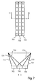
- FIG 7 Yet another embodiment of the present invention is illustrated in figure 7 and comprises three parallel linear arrays of light emitting diodes; one array 701 of red LEDs, one array 702 of green LEDs and one array 703 of blue LEDs.
- a brightness enhancing means is arranged on the arrays.
- the light from the red LEDs 701 is collimated by a collimating means defined by the sidewalls 711 and 712
- the light from the green LEDs 702 is collimated by a collimating means defined by the sidewalls 721 and 722
- the light from the blue LEDs 703 is collimated by a collimating means defined by the sidewalls 731 and 732.
- the sidewall 711 should reflect red light, but may also reflect light of any other color, and the sidewall 712 should reflect red light.
- the sidewall 721 should reflect green light, but may also reflect blue light, and the sidewall 722 should reflect green light but may also reflect red light.
- the sidewall 731 should reflect blue light but may also reflect light of any other color, and the sidewall 732 should reflect blue light.
- the output areas of the three different collimating means overlap to essentially 100 %.
- the sidewalls 711, 721 and 732 all meet at the peripheral boundary of the brightness enhancing means that is defined by the sidewall 711. Thus, the limits of the output areas of the three collimating means coincide with this peripheral boundary.
- the sidewalls 712, 722 and 731 all meet at the peripheral boundary of the brightness enhancing means that is defined by the sidewall 731.
- the limits of the output areas of the three collimating means coincide with this peripheral boundary.
- a good color mixing is provided at the peripheral boundary defined by the sidewall 731.
- a device as shown in figure 7 is not limited to the use of three lighting units.
- a device comprising more than three lighting units for example devices as illustrated in figure 1 or 4 , may also make use of this approach of obtaining good color mixing at the peripheral boundaries of the brightness enhancing means, by arranging the collimating means of the brightness enhancing means such that the output areas of the two or more collimating means located closest to a peripheral boundary, taken in a direction perpendicular to the boundary, extend to the peripheral boundary, i.e. the limits of these two or more output areas partly coincide with the peripheral boundary.
- each lighting unit in a light-emitting device of the present invention may very well comprise a plurality of light-emitting diodes. However, as will be appreciated by those skilled in the art, it is not necessary to use more than one light emitting diode in each lighting unit.
- a plurality of devices of the invention may be arranged adjacent to each other.
- a four-color light emitting device and a brightness enhancing means adapted for this device are illustrated in figure 9 .
- the light source array forms a row-column matrix 901.
- a first layer of brightness enhancing means 906 is arranged on the LED matrix.
- Reflective walls 909 are preferably arranged between adjacent collimating means (parallel to the rows in the LED matrix) in the first layer.
- This first layer of brightness enhancing means provides collimation and color mixing in the dimension of the rows (y-dimension), but essentially not in the dimension of the columns (x-dimension) in the LED matrix.
- a second layer 910 of brightness enhancing means is arranged on the top of the first layer 906 of brightness enhancing means.
- This second layer 910 is a brightness enhancing means comprising collimating means of two types, where the first type reflects light of the first and second color, and the second type reflects light of the third and fourth color.
- this second layer brightness enhancing means 910 provides collimation and color mixing in the dimension of the columns (x-dimension) of the LED matrix.
- the first and the second layer of brightness enhancing means provides collimation and color mixing in both the dimension of the columns (x) and that of the rows (y) of the LED matrix.
- all lighting units LEDs are arranged at equal distances from each other, where the overlap between adjacent output areas is essentially the same over essentially the whole device.
- the distance between adjacent lighting units and/or the overlap between adjacent output areas is equal over the whole device.
- the light-emitting device is divided into a plurality of subgroups, e.g. pixels.
- Each pixel comprises a plurality of lighting units, e.g. LEDs.
- the distance between adjacent lighting units is the same, and the overlap between adjacent output areas is the same.
- the distance between two adjacent lighting units, where the two are comprised in different sub-groups is bigger than the distance inside a sub-group, and in addition, the overlap between the output areas corresponding to the two adjacent lighting units is smaller than the overlap inside a subgroup.
- a brightness enhancing means of the present invention may be used to mix and couple the light emitted by an array of light emitting diodes into a wave-guide.
- a light-emitting device of the present invention may comprise more than one brightness-enhancing means arranged on the light emitting diodes. For example when using certain types of LEDs, light is emitted from these in at least two general directions, and in such cases, it may be desired to use one brightness-enhancing means in each of those directions.
- a reflecting surface such as a mirror or the like, may be arranged at the output areas of the brightness enhancing means in order to reflect light exiting the device into another general direction.
- a reflecting surface such as a mirror or the like
- the output areas of the two separate brightness enhancing means are facing in generally opposite directions.
- Light-emitting devices of the present invention may be used in several different applications. Such applications include, but are not limited to, linear light-sources, light-sources in high brightness lamps, such as room lighting, ambient lighting, stage lighting, traffic lights, vehicle lamps and backlights in LCD based display devices.
- the brightness enhancing means of the present invention may also be used in an LED display device, for example to direct the light from the LEDs and to obtain a good color mixing.
- Another example is the use as light source in a projection LCD display.
- a brightness enhancing means of the present invention may be used to mix and couple the light emitted by an array of light emitting diodes into a wave-guide, by arranging a wave-guide to receive light from the output areas of the brightness enhancing means.
- a light-emitting device of the present invention may comprise more than one brightness-enhancing means arranged on the light emitting diodes. For example when using side emissive LEDs, light is emitted from these in at least two general directions. In such cases, it may be desired to use one brightness-enhancing means in each of those directions.
- a brightness enhancing means of the present embodiment may also be adapted to individually collimate light of more than three different colors.
- an array of LEDs of four or more different colors may also be provided with a brightness enhancing means of the present invention, either where each different LED corresponds to a separate collimating means or where one collimating means corresponds to two or more LEDs of different colors.
- the present invention is not limited to the use of light emitting diodes as the source of light.
- other light-emitting devices may be used, such as incandescent bulbs, discharge lamps, fluorescent tubes, etc.
- the above-mentioned embodiments relate mainly to collimation and color mixing of light in the visible or near visible wavelength range (UV to IR).
- the brightness enhancing means of the present invention may also be for collimation of electromagnetic radiation outside this wavelength range, such as for example X-ray radiation, by choosing suitable dichroic filters.
Landscapes
- Physics & Mathematics (AREA)
- General Physics & Mathematics (AREA)
- Optics & Photonics (AREA)
- Nonlinear Science (AREA)
- Mathematical Physics (AREA)
- Chemical & Material Sciences (AREA)
- Crystallography & Structural Chemistry (AREA)
- Electroluminescent Light Sources (AREA)
- Led Device Packages (AREA)
- Planar Illumination Modules (AREA)
- Optical Elements Other Than Lenses (AREA)
- Measuring Pulse, Heart Rate, Blood Pressure Or Blood Flow (AREA)
Claims (23)
- Moyen d'amélioration de luminosité (5), comprenant au moins un premier moyen de collimation (6) et au moins un deuxième moyen de collimation (7) ayant chacun une zone de réception (61, 71), une zone de sortie (62, 72) plus grande que ladite zone de réception (61, 71) et des parois latérales (63, 73) s'étendant au moins partiellement entre lesdites zones de réception et de sortie, dans lequel
au moins une portion des parois latérales (63) dudit premier moyen de collimation (6) comprend un premier filtre agencé pour réfléchir une lumière d'une première propriété de lumière, laquelle lumière est reçue par l'intermédiaire de ladite zone de réception (61) dudit premier moyen de collimation (6), vers ladite zone de sortie (62) dudit premier moyen de collimation (6), au moins une portion des parois latérales (73) dudit deuxième moyen de collimation (7) comprend un deuxième filtre agencé pour réfléchir une lumière d'une deuxième propriété de lumière, laquelle lumière est reçue par l'intermédiaire de ladite zone de réception (71) dudit deuxième moyen de collimation (7), vers ladite zone de sortie (72) dudit deuxième moyen de collimation (7),
dans lequel la zone de sortie (62) dudit premier moyen de collimation et la zone de sortie (72) dudit deuxième moyen de collimation se chevauchent au moins partiellement, caractérisé en ce que
ladite première propriété de lumière est une première plage de longueurs d'ondes, et ledit premier filtre est un premier filtre dichroïque, et ladite deuxième propriété de lumière est une deuxième plage de longueurs d'ondes, et ledit deuxième filtre est un deuxième filtre dichroïque, ou
ladite première propriété de lumière est un premier état de polarisation, et ledit premier filtre est un premier filtre de polarisation, et ladite deuxième propriété de lumière est un deuxième état de polarisation, et ledit deuxième filtre est un deuxième filtre de polarisation ; et
ladite première propriété de lumière est différente de ladite deuxième propriété de lumière. - Moyen d'amélioration de luminosité selon la revendication 1, dans lequel l'angle entre la normale à la zone de réception et la normale à ladite portion des parois latérales dudit moyen de collimation, laquelle portion comprenant ledit filtre, est sensiblement constant avec la distance de la zone de réception.
- Moyen d'amélioration de luminosité selon la revendication 1, dans lequel l'angle entre la normale à la zone de réception et la normale à ladite portion des parois latérales dudit moyen de collimation, laquelle portion comprenant ledit filtre, augmente avec la distance de la zone de réception.
- Moyen d'amélioration de luminosité selon l'une quelconque des revendications précédentes, dans lequel le chevauchement des zones de sortie de deux moyens de collimation adjacents est d'au moins 10%.
- Moyen d'amélioration de luminosité selon l'une quelconque des revendications précédentes, dans lequel lesdites parois latérales comprennent des éléments muraux autoporteurs.
- Moyen d'amélioration de luminosité selon la revendication 5, dans lequel ledit filtre comprend un premier matériau de filtre agencé sur un premier côté desdits éléments muraux et un deuxième matériau de filtre agencé sur un deuxième côté desdits éléments muraux.
- Moyen d'amélioration de luminosité selon l'une quelconque des revendications précédentes, dans lequel un moyen de blocage de lumière (101) est agencé sur au moins une partie des zones de sortie d'au moins une partie du moyen de collimation situé à une frontière périphérique dudit moyen d'amélioration de luminosité.
- Moyen d'amélioration de luminosité selon l'une quelconque des revendications précédentes, dans lequel les limites des zones de sortie (801, 802) des au moins deux moyens de collimation les plus proches d'une frontière périphérique (804) dudit moyen d'amélioration de luminosité, prises dans une direction perpendiculaire à ladite frontière périphérique (804), coïncident au moins partiellement avec ladite frontière périphérique (804).
- Moyen d'amélioration de luminosité selon l'une quelconque des revendications précédentes, dans lequel au moins des portions des parois latérales formant ou faisant face à une frontière périphérique (804) dudit moyen d'amélioration de luminosité comprennent une surface réfléchissante sur tout le spectre.
- Dispositif électroluminescent comprenant une première unité d'éclairage (2) pour émettre une lumière d'une première propriété de lumière et une deuxième unité d'éclairage (3) pour émettre une lumière d'une deuxième propriété de lumière agencées sur un substrat (1), ledit dispositif électroluminescent comprenant en outre le moyen d'amélioration de luminosité (5) selon la revendication 1 agencé pour recevoir la lumière émise par ladite première unité d'éclairage (2) et la lumière émise par ladite deuxième unité d'éclairage (3).
- Dispositif électroluminescent selon la revendication 10, dans lequel ledit moyen d'amélioration de luminosité (5) est défini selon l'une quelconque des revendications 2 à 9.
- Dispositif électroluminescent selon la revendication 10 ou 11, dans lequel un ralentisseur (9) est agencé sur lesdites unités d'éclairage (2, 3), un réflecteur de polarisation (10) est agencé sur ledit ralentisseur (9), et ledit moyen d'amélioration de luminosité est agencé sur ledit réflecteur de polarisation (10).
- Dispositif électroluminescent selon l'une quelconque des revendications 10 à 12, dans lequel ledit substrat (1) est un substrat réfléchissant.
- Dispositif électroluminescent selon l'une quelconque des revendications 10 à 13, dans lequel un collimateur (12, 13) est agencé sur lesdites unités d'éclairage (2, 3) pour recevoir et collimater la lumière émise par lesdites unités d'éclairage, et ledit moyen d'amélioration de luminosité (5) est agencé sur ledit collimateur.
- Dispositif électroluminescent selon l'une quelconque des revendications 10 à 14, dans lequel lesdites unités d'éclairage comprennent des diodes électroluminescentes.
- Dispositif électroluminescent selon la revendication 15, dans lequel lesdites diodes électroluminescentes comprennent des diodes électroluminescentes organiques.
- Dispositif électroluminescent selon la revendication 15 ou 16, dans lequel ladite première unité d'éclairage comprend au moins une diode électroluminescente et ladite deuxième unité d'éclairage comprend au moins une diode électroluminescente.
- Dispositif électroluminescent selon la revendication 17, dans lequel ladite première unité d'éclairage comprend un premier réseau linéaire de deux diodes électroluminescentes ou plus et ladite deuxième unité d'éclairage comprend un deuxième réseau linéaire de deux diodes électroluminescentes ou plus, ledit premier réseau et ledit deuxième réseau étant sensiblement parallèles.
- Dispositif électroluminescent selon l'une quelconque des revendications 10 à 18, dans lequel la sortie de lumière à une frontière périphérique dudit dispositif est au moins partiellement réduite.
- Dispositif électroluminescent selon la revendication 19, dans lequel ladite sortie de lumière est réduite en réduisant le flux de lumière émise par au moins une partie des unités d'éclairage situées à une frontière périphérique dudit dispositif.
- Dispositif électroluminescent selon l'une quelconque des revendications 10 à 20, comprenant en outre un guide d'ondes, dans lequel ledit moyen d'amélioration de luminosité est agencé pour coupler la lumière émise par ladite première unité d'éclairage et la lumière émise par ladite deuxième unité d'éclairage dans ledit guide d'ondes.
- Dispositif d'affichage comprenant un moyen d'amélioration de luminosité selon l'une quelconque des revendications 1 à 9 ou un dispositif électroluminescent selon l'une quelconque des revendications 10 à 21.
- Dispositif d'affichage par projection comprenant un moyen d'amélioration de luminosité selon l'une quelconque des revendications 1 à 9 ou un dispositif électroluminescent selon l'une quelconque des revendications 10 à 21.
Priority Applications (1)
| Application Number | Priority Date | Filing Date | Title |
|---|---|---|---|
| EP06744977A EP1891476B1 (fr) | 2005-05-30 | 2006-05-18 | Dispositif electroluminescent a couche d'amelioration de la luminosite |
Applications Claiming Priority (4)
| Application Number | Priority Date | Filing Date | Title |
|---|---|---|---|
| EP05104598 | 2005-05-30 | ||
| EP05109499 | 2005-10-12 | ||
| PCT/IB2006/051580 WO2006129220A1 (fr) | 2005-05-30 | 2006-05-18 | Dispositif electroluminescent a couche d'amelioration de la luminosite |
| EP06744977A EP1891476B1 (fr) | 2005-05-30 | 2006-05-18 | Dispositif electroluminescent a couche d'amelioration de la luminosite |
Publications (2)
| Publication Number | Publication Date |
|---|---|
| EP1891476A1 EP1891476A1 (fr) | 2008-02-27 |
| EP1891476B1 true EP1891476B1 (fr) | 2012-12-19 |
Family
ID=37004654
Family Applications (1)
| Application Number | Title | Priority Date | Filing Date |
|---|---|---|---|
| EP06744977A Not-in-force EP1891476B1 (fr) | 2005-05-30 | 2006-05-18 | Dispositif electroluminescent a couche d'amelioration de la luminosite |
Country Status (7)
| Country | Link |
|---|---|
| US (1) | US7942537B2 (fr) |
| EP (1) | EP1891476B1 (fr) |
| JP (1) | JP5049272B2 (fr) |
| KR (1) | KR101280901B1 (fr) |
| CN (1) | CN101189543B (fr) |
| TW (1) | TW200703721A (fr) |
| WO (1) | WO2006129220A1 (fr) |
Families Citing this family (44)
| Publication number | Priority date | Publication date | Assignee | Title |
|---|---|---|---|---|
| JP4535504B2 (ja) * | 2005-11-02 | 2010-09-01 | シチズン電子株式会社 | 照明用レンズの構造。 |
| JP5008209B2 (ja) * | 2006-07-31 | 2012-08-22 | コーニンクレッカ フィリップス エレクトロニクス エヌ ヴィ | 光放出装置 |
| CN101529308A (zh) * | 2006-10-20 | 2009-09-09 | 皇家飞利浦电子股份有限公司 | 具有准直结构的发光设备 |
| EP2179320A1 (fr) * | 2007-08-10 | 2010-04-28 | Koninklijke Philips Electronics N.V. | Dispositif d'éclairage |
| CN101815960B (zh) * | 2007-08-10 | 2012-06-13 | 皇家飞利浦电子股份有限公司 | 照明设备 |
| RU2489742C2 (ru) | 2007-08-10 | 2013-08-10 | Конинклейке Филипс Электроникс Н.В. | Осветительное устройство |
| JP4938611B2 (ja) * | 2007-10-09 | 2012-05-23 | アルプス電気株式会社 | 半導体発光装置 |
| EP2065752A1 (fr) * | 2007-11-23 | 2009-06-03 | Koninklijke Philips Electronics N.V. | Appareil d'éclairage optique pour illuminer un échantillon avec un faisceau linéaire |
| JP4570668B2 (ja) * | 2008-06-27 | 2010-10-27 | 財団法人山形県産業技術振興機構 | 照明装置 |
| JP2010134217A (ja) * | 2008-12-05 | 2010-06-17 | Sony Corp | カラーフィルタおよびその製造方法並びに発光装置 |
| CN101839420B (zh) * | 2009-03-20 | 2013-05-29 | 北京京东方光电科技有限公司 | 背光模组 |
| US8475002B2 (en) | 2009-05-01 | 2013-07-02 | Lighting Science Group Corporation | Sustainable outdoor lighting system and associated methods |
| US8308318B2 (en) | 2009-05-01 | 2012-11-13 | Lighting Science Group Corporation | Sustainable outdoor lighting system |
| JP5569132B2 (ja) * | 2009-05-15 | 2014-08-13 | 株式会社ニコン | 測距装置および撮像装置 |
| TWM367356U (en) * | 2009-06-04 | 2009-10-21 | Delta Electronics Inc | LED light source module and projection device comprising the same |
| TWI416488B (zh) * | 2009-09-14 | 2013-11-21 | Au Optronics Corp | 畫素資料的補償方法、時序控制器以及液晶顯示器 |
| CN102116438B (zh) * | 2009-12-30 | 2012-11-21 | 中强光电股份有限公司 | 发光装置与投影机 |
| EP2402814A1 (fr) * | 2010-06-30 | 2012-01-04 | Koninklijke Philips Electronics N.V. | Dispositif d'affichage autostéréoscopique |
| CN103068301A (zh) * | 2010-08-24 | 2013-04-24 | 欧司朗有限公司 | 荧光装置以及包括其的照明设备 |
| WO2012025144A1 (fr) * | 2010-08-24 | 2012-03-01 | Osram Ag | Dispositif luminescent et appareil d'éclairage comprenant celui-ci |
| JP2013065521A (ja) * | 2011-09-20 | 2013-04-11 | Minebea Co Ltd | 配光制御部材及びそれを用いた照明装置 |
| US8841831B2 (en) * | 2012-03-13 | 2014-09-23 | Panasonic Corporation | Light emitting device, and illumination apparatus and luminaire using same |
| US8899775B2 (en) | 2013-03-15 | 2014-12-02 | Lighting Science Group Corporation | Low-angle thoroughfare surface lighting device |
| US8899776B2 (en) | 2012-05-07 | 2014-12-02 | Lighting Science Group Corporation | Low-angle thoroughfare surface lighting device |
| WO2014033602A2 (fr) * | 2012-08-31 | 2014-03-06 | Koninklijke Philips N.V. | Dispositif d'éclairage reposant sur un guide de lumière comprenant des particules dispersant de la lumière et module de sélection d'angle de lumière |
| US9435500B2 (en) | 2012-12-04 | 2016-09-06 | Lighting Science Group Corporation | Modular segmented electronics assembly |
| US9885461B2 (en) | 2015-04-09 | 2018-02-06 | Robe Lighting S.R.O. | Homogenization system for an LED luminaire |
| CN111006141A (zh) * | 2013-01-14 | 2020-04-14 | 罗布照明公司 | 用于led照明设备的改进的均化系统 |
| CN104037191B (zh) * | 2013-03-06 | 2017-03-01 | 瀚宇彩晶股份有限公司 | 显示面板与其制造方法 |
| US9255670B2 (en) | 2013-03-15 | 2016-02-09 | Lighting Science Group Corporation | Street lighting device for communicating with observers and associated methods |
| WO2015050964A1 (fr) * | 2013-10-03 | 2015-04-09 | 3M Innovative Properties Company | Système d'éclairage à distance |
| WO2015061092A1 (fr) * | 2013-10-25 | 2015-04-30 | 3M Innovative Properties Company | Installations de lampe modulaire à intensité élevée |
| US10234129B2 (en) | 2014-10-24 | 2019-03-19 | Lighting Science Group Corporation | Modular street lighting system |
| US9775514B2 (en) | 2015-02-26 | 2017-10-03 | Canon Kabushiki Kaisha | Apparatus for measurement of a fundus comprising a focusing system and a wavefront correction device |
| KR101795218B1 (ko) * | 2016-03-07 | 2017-11-08 | 현대자동차주식회사 | 차량용 조명 장치 |
| US10119676B2 (en) * | 2016-06-10 | 2018-11-06 | Osram Gmbh | Lighting device, corresponding lamp and method |
| US10384803B2 (en) * | 2016-10-07 | 2019-08-20 | The Boeing Company | Methods and devices for light distribution in an aircraft, and aircraft including such devices |
| EP3560295B1 (fr) * | 2016-12-20 | 2020-08-26 | Signify Holding B.V. | Spot polarisé multimode avec un état de polarisation réglable électriquement |
| CN108267883A (zh) * | 2018-01-24 | 2018-07-10 | 京东方科技集团股份有限公司 | 一种彩膜基板、其制作方法及显示面板 |
| TWI706197B (zh) * | 2019-02-01 | 2020-10-01 | 明基材料股份有限公司 | 有機發光二極體顯示器 |
| CN109656118B (zh) | 2019-02-26 | 2021-08-24 | 京东方科技集团股份有限公司 | 全息显示装置及电子设备 |
| US10883704B2 (en) | 2019-03-29 | 2021-01-05 | Robe Lighting S.R.O. | Homogenization system for an LED luminaire |
| JP7217668B2 (ja) | 2019-05-27 | 2023-02-03 | 株式会社日立ハイテク | 光源および生化学分析装置 |
| WO2023194157A1 (fr) * | 2022-04-04 | 2023-10-12 | Signify Holding B.V. | Lèche-murs à éclairage désinfectant ayant une sécurité et une performance améliorées |
Family Cites Families (17)
| Publication number | Priority date | Publication date | Assignee | Title |
|---|---|---|---|---|
| JPH10268292A (ja) | 1997-01-21 | 1998-10-09 | Sharp Corp | カラーフィルタ基板およびカラー液晶表示素子 |
| US6654082B1 (en) | 1998-09-16 | 2003-11-25 | Optrex Corporation | Liquid crystal display element and color display device having particular transflector |
| JP2000194286A (ja) | 1998-12-28 | 2000-07-14 | Fujitsu Ltd | カラ―表示装置 |
| TW380213B (en) * | 1999-01-21 | 2000-01-21 | Ind Tech Res Inst | Illumination apparatus and image projection apparatus includes the same |
| US6527411B1 (en) * | 2000-08-01 | 2003-03-04 | Visteon Corporation | Collimating lamp |
| JP4708537B2 (ja) * | 2000-08-10 | 2011-06-22 | キヤノン株式会社 | 画像表示装置および画像表示システム |
| WO2002047915A1 (fr) | 2000-12-12 | 2002-06-20 | Creo Il. Ltd. | Tete d'imagerie dotee d'un reseau de diodes laser et d'un reseau de tuyau de microlumiere pour la formation de faisceau |
| JP4178840B2 (ja) | 2002-06-07 | 2008-11-12 | 日亜化学工業株式会社 | 面状発光光源、直下型バックライト、およびそれを用いた信号灯 |
| JP3960377B2 (ja) * | 2002-07-19 | 2007-08-15 | Necディスプレイソリューションズ株式会社 | 光源装置及び投写型表示装置 |
| JP3551187B2 (ja) * | 2002-11-28 | 2004-08-04 | セイコーエプソン株式会社 | 光学素子及び照明装置並びに投射型表示装置 |
| US7369268B2 (en) * | 2003-01-14 | 2008-05-06 | Eastman Kodak Company | Light source using large area LEDs |
| WO2004068182A2 (fr) | 2003-01-24 | 2004-08-12 | Digital Optics International Corporation | Systeme d'eclairage haute densite |
| JP4596746B2 (ja) * | 2003-04-17 | 2010-12-15 | 富士フイルム株式会社 | 光学素子、光学系および投映プロジェクタ装置 |
| TW200502640A (en) | 2003-07-02 | 2005-01-16 | Au Optronics Corp | Back light module |
| US20050002204A1 (en) | 2003-07-04 | 2005-01-06 | Kun-Lung Lin | Module for uniforming light |
| US7083304B2 (en) * | 2003-08-01 | 2006-08-01 | Illumination Management Solutions, Inc. | Apparatus and method of using light sources of differing wavelengths in an unitized beam |
| KR100813253B1 (ko) * | 2006-04-27 | 2008-03-13 | 삼성전자주식회사 | 고효율의 편광도광판 유닛, 이를 채용한 백라이트 유닛 및디스플레이 장치 |
-
2006
- 2006-05-18 EP EP06744977A patent/EP1891476B1/fr not_active Not-in-force
- 2006-05-18 KR KR1020077030721A patent/KR101280901B1/ko not_active Expired - Fee Related
- 2006-05-18 WO PCT/IB2006/051580 patent/WO2006129220A1/fr not_active Ceased
- 2006-05-18 JP JP2008514247A patent/JP5049272B2/ja not_active Expired - Fee Related
- 2006-05-18 US US11/916,213 patent/US7942537B2/en not_active Expired - Fee Related
- 2006-05-18 CN CN2006800192522A patent/CN101189543B/zh not_active Expired - Fee Related
- 2006-05-26 TW TW095118814A patent/TW200703721A/zh unknown
Also Published As
| Publication number | Publication date |
|---|---|
| US20080192457A1 (en) | 2008-08-14 |
| EP1891476A1 (fr) | 2008-02-27 |
| KR20080020646A (ko) | 2008-03-05 |
| WO2006129220A1 (fr) | 2006-12-07 |
| US7942537B2 (en) | 2011-05-17 |
| KR101280901B1 (ko) | 2013-07-02 |
| TW200703721A (en) | 2007-01-16 |
| JP5049272B2 (ja) | 2012-10-17 |
| CN101189543A (zh) | 2008-05-28 |
| JP2008546015A (ja) | 2008-12-18 |
| CN101189543B (zh) | 2011-08-10 |
Similar Documents
| Publication | Publication Date | Title |
|---|---|---|
| EP1891476B1 (fr) | Dispositif electroluminescent a couche d'amelioration de la luminosite | |
| CN114730044B (zh) | 定向照明设备和隐私显示器 | |
| US7883238B2 (en) | Light collimation and mixing of remote light sources | |
| TWI530732B (zh) | 發光結構 | |
| CN100410770C (zh) | 面照明装置和具有该装置的液晶显示装置 | |
| US20100033954A1 (en) | Thin illumination device, display device and luminary device | |
| WO2007027529A2 (fr) | Procedes permettant de former des panneaux lumineux a eclairage direct comprenant une cavite de recyclage de la lumiere munie d'un transflecteur concave | |
| JP2010507245A (ja) | コリメート化構造体を有する発光デバイス | |
| WO2019159462A1 (fr) | Dispositif d'éclairage | |
| US7866849B2 (en) | Light-emitting device | |
| JP2017117531A (ja) | 照明装置及び表示装置 | |
| US20090316397A1 (en) | Light-emitting device | |
| JP4789026B1 (ja) | 混色照明装置 | |
| JP4789027B1 (ja) | 混色照明装置 | |
| JP2013152811A (ja) | 照明装置、表示装置、及びテレビ受信装置 | |
| CN120972418A (zh) | 显示装置 | |
| JP2013161636A (ja) | 照明装置、表示装置、及びテレビ受信装置 |
Legal Events
| Date | Code | Title | Description |
|---|---|---|---|
| PUAI | Public reference made under article 153(3) epc to a published international application that has entered the european phase |
Free format text: ORIGINAL CODE: 0009012 |
|
| 17P | Request for examination filed |
Effective date: 20080102 |
|
| AK | Designated contracting states |
Kind code of ref document: A1 Designated state(s): AT BE BG CH CY CZ DE DK EE ES FI FR GB GR HU IE IS IT LI LT LU LV MC NL PL PT RO SE SI SK TR |
|
| DAX | Request for extension of the european patent (deleted) | ||
| 17Q | First examination report despatched |
Effective date: 20081125 |
|
| GRAP | Despatch of communication of intention to grant a patent |
Free format text: ORIGINAL CODE: EPIDOSNIGR1 |
|
| GRAS | Grant fee paid |
Free format text: ORIGINAL CODE: EPIDOSNIGR3 |
|
| GRAA | (expected) grant |
Free format text: ORIGINAL CODE: 0009210 |
|
| AK | Designated contracting states |
Kind code of ref document: B1 Designated state(s): AT BE BG CH CY CZ DE DK EE ES FI FR GB GR HU IE IS IT LI LT LU LV MC NL PL PT RO SE SI SK TR |
|
| REG | Reference to a national code |
Ref country code: GB Ref legal event code: FG4D |
|
| REG | Reference to a national code |
Ref country code: CH Ref legal event code: EP |
|
| REG | Reference to a national code |
Ref country code: AT Ref legal event code: REF Ref document number: 589672 Country of ref document: AT Kind code of ref document: T Effective date: 20130115 |
|
| REG | Reference to a national code |
Ref country code: DE Ref legal event code: R096 Ref document number: 602006033700 Country of ref document: DE Effective date: 20130207 |
|
| PG25 | Lapsed in a contracting state [announced via postgrant information from national office to epo] |
Ref country code: SE Free format text: LAPSE BECAUSE OF FAILURE TO SUBMIT A TRANSLATION OF THE DESCRIPTION OR TO PAY THE FEE WITHIN THE PRESCRIBED TIME-LIMIT Effective date: 20121219 Ref country code: FI Free format text: LAPSE BECAUSE OF FAILURE TO SUBMIT A TRANSLATION OF THE DESCRIPTION OR TO PAY THE FEE WITHIN THE PRESCRIBED TIME-LIMIT Effective date: 20121219 Ref country code: LT Free format text: LAPSE BECAUSE OF FAILURE TO SUBMIT A TRANSLATION OF THE DESCRIPTION OR TO PAY THE FEE WITHIN THE PRESCRIBED TIME-LIMIT Effective date: 20121219 Ref country code: ES Free format text: LAPSE BECAUSE OF FAILURE TO SUBMIT A TRANSLATION OF THE DESCRIPTION OR TO PAY THE FEE WITHIN THE PRESCRIBED TIME-LIMIT Effective date: 20130330 |
|
| REG | Reference to a national code |
Ref country code: NL Ref legal event code: VDEP Effective date: 20121219 Ref country code: AT Ref legal event code: MK05 Ref document number: 589672 Country of ref document: AT Kind code of ref document: T Effective date: 20121219 |
|
| REG | Reference to a national code |
Ref country code: LT Ref legal event code: MG4D |
|
| PG25 | Lapsed in a contracting state [announced via postgrant information from national office to epo] |
Ref country code: SI Free format text: LAPSE BECAUSE OF FAILURE TO SUBMIT A TRANSLATION OF THE DESCRIPTION OR TO PAY THE FEE WITHIN THE PRESCRIBED TIME-LIMIT Effective date: 20121219 Ref country code: GR Free format text: LAPSE BECAUSE OF FAILURE TO SUBMIT A TRANSLATION OF THE DESCRIPTION OR TO PAY THE FEE WITHIN THE PRESCRIBED TIME-LIMIT Effective date: 20130320 Ref country code: LV Free format text: LAPSE BECAUSE OF FAILURE TO SUBMIT A TRANSLATION OF THE DESCRIPTION OR TO PAY THE FEE WITHIN THE PRESCRIBED TIME-LIMIT Effective date: 20121219 |
|
| PG25 | Lapsed in a contracting state [announced via postgrant information from national office to epo] |
Ref country code: BE Free format text: LAPSE BECAUSE OF FAILURE TO SUBMIT A TRANSLATION OF THE DESCRIPTION OR TO PAY THE FEE WITHIN THE PRESCRIBED TIME-LIMIT Effective date: 20121219 Ref country code: BG Free format text: LAPSE BECAUSE OF FAILURE TO SUBMIT A TRANSLATION OF THE DESCRIPTION OR TO PAY THE FEE WITHIN THE PRESCRIBED TIME-LIMIT Effective date: 20130319 Ref country code: IS Free format text: LAPSE BECAUSE OF FAILURE TO SUBMIT A TRANSLATION OF THE DESCRIPTION OR TO PAY THE FEE WITHIN THE PRESCRIBED TIME-LIMIT Effective date: 20130419 Ref country code: EE Free format text: LAPSE BECAUSE OF FAILURE TO SUBMIT A TRANSLATION OF THE DESCRIPTION OR TO PAY THE FEE WITHIN THE PRESCRIBED TIME-LIMIT Effective date: 20121219 Ref country code: CZ Free format text: LAPSE BECAUSE OF FAILURE TO SUBMIT A TRANSLATION OF THE DESCRIPTION OR TO PAY THE FEE WITHIN THE PRESCRIBED TIME-LIMIT Effective date: 20121219 Ref country code: AT Free format text: LAPSE BECAUSE OF FAILURE TO SUBMIT A TRANSLATION OF THE DESCRIPTION OR TO PAY THE FEE WITHIN THE PRESCRIBED TIME-LIMIT Effective date: 20121219 Ref country code: CY Free format text: LAPSE BECAUSE OF FAILURE TO SUBMIT A TRANSLATION OF THE DESCRIPTION OR TO PAY THE FEE WITHIN THE PRESCRIBED TIME-LIMIT Effective date: 20121219 Ref country code: SK Free format text: LAPSE BECAUSE OF FAILURE TO SUBMIT A TRANSLATION OF THE DESCRIPTION OR TO PAY THE FEE WITHIN THE PRESCRIBED TIME-LIMIT Effective date: 20121219 |
|
| PG25 | Lapsed in a contracting state [announced via postgrant information from national office to epo] |
Ref country code: PT Free format text: LAPSE BECAUSE OF FAILURE TO SUBMIT A TRANSLATION OF THE DESCRIPTION OR TO PAY THE FEE WITHIN THE PRESCRIBED TIME-LIMIT Effective date: 20130419 Ref country code: RO Free format text: LAPSE BECAUSE OF FAILURE TO SUBMIT A TRANSLATION OF THE DESCRIPTION OR TO PAY THE FEE WITHIN THE PRESCRIBED TIME-LIMIT Effective date: 20121219 Ref country code: PL Free format text: LAPSE BECAUSE OF FAILURE TO SUBMIT A TRANSLATION OF THE DESCRIPTION OR TO PAY THE FEE WITHIN THE PRESCRIBED TIME-LIMIT Effective date: 20121219 Ref country code: NL Free format text: LAPSE BECAUSE OF FAILURE TO SUBMIT A TRANSLATION OF THE DESCRIPTION OR TO PAY THE FEE WITHIN THE PRESCRIBED TIME-LIMIT Effective date: 20121219 |
|
| REG | Reference to a national code |
Ref country code: CH Ref legal event code: PFA Owner name: KONINKLIJKE PHILIPS N.V., NL Free format text: FORMER OWNER: KONINKLIJKE PHILIPS ELECTRONICS N.V., NL |
|
| RAP2 | Party data changed (patent owner data changed or rights of a patent transferred) |
Owner name: KONINKLIJKE PHILIPS N.V. |
|
| PLBE | No opposition filed within time limit |
Free format text: ORIGINAL CODE: 0009261 |
|
| STAA | Information on the status of an ep patent application or granted ep patent |
Free format text: STATUS: NO OPPOSITION FILED WITHIN TIME LIMIT |
|
| PG25 | Lapsed in a contracting state [announced via postgrant information from national office to epo] |
Ref country code: DK Free format text: LAPSE BECAUSE OF FAILURE TO SUBMIT A TRANSLATION OF THE DESCRIPTION OR TO PAY THE FEE WITHIN THE PRESCRIBED TIME-LIMIT Effective date: 20121219 |
|
| 26N | No opposition filed |
Effective date: 20130920 |
|
| PG25 | Lapsed in a contracting state [announced via postgrant information from national office to epo] |
Ref country code: IT Free format text: LAPSE BECAUSE OF FAILURE TO SUBMIT A TRANSLATION OF THE DESCRIPTION OR TO PAY THE FEE WITHIN THE PRESCRIBED TIME-LIMIT Effective date: 20121219 Ref country code: MC Free format text: LAPSE BECAUSE OF FAILURE TO SUBMIT A TRANSLATION OF THE DESCRIPTION OR TO PAY THE FEE WITHIN THE PRESCRIBED TIME-LIMIT Effective date: 20121219 |
|
| REG | Reference to a national code |
Ref country code: CH Ref legal event code: PL |
|
| REG | Reference to a national code |
Ref country code: DE Ref legal event code: R097 Ref document number: 602006033700 Country of ref document: DE Effective date: 20130920 |
|
| PG25 | Lapsed in a contracting state [announced via postgrant information from national office to epo] |
Ref country code: CH Free format text: LAPSE BECAUSE OF NON-PAYMENT OF DUE FEES Effective date: 20130531 Ref country code: LI Free format text: LAPSE BECAUSE OF NON-PAYMENT OF DUE FEES Effective date: 20130531 |
|
| REG | Reference to a national code |
Ref country code: IE Ref legal event code: MM4A |
|
| PG25 | Lapsed in a contracting state [announced via postgrant information from national office to epo] |
Ref country code: IE Free format text: LAPSE BECAUSE OF NON-PAYMENT OF DUE FEES Effective date: 20130518 |
|
| REG | Reference to a national code |
Ref country code: DE Ref legal event code: R081 Ref document number: 602006033700 Country of ref document: DE Owner name: PHILIPS LIGHTING HOLDING B.V., NL Free format text: FORMER OWNER: KONINKLIJKE PHILIPS ELECTRONICS N.V., EINDHOVEN, NL Effective date: 20140328 Ref country code: DE Ref legal event code: R081 Ref document number: 602006033700 Country of ref document: DE Owner name: KONINKLIJKE PHILIPS N.V., NL Free format text: FORMER OWNER: KONINKLIJKE PHILIPS ELECTRONICS N.V., EINDHOVEN, NL Effective date: 20140328 |
|
| PG25 | Lapsed in a contracting state [announced via postgrant information from national office to epo] |
Ref country code: TR Free format text: LAPSE BECAUSE OF FAILURE TO SUBMIT A TRANSLATION OF THE DESCRIPTION OR TO PAY THE FEE WITHIN THE PRESCRIBED TIME-LIMIT Effective date: 20121219 |
|
| PG25 | Lapsed in a contracting state [announced via postgrant information from national office to epo] |
Ref country code: LU Free format text: LAPSE BECAUSE OF NON-PAYMENT OF DUE FEES Effective date: 20130518 Ref country code: HU Free format text: LAPSE BECAUSE OF FAILURE TO SUBMIT A TRANSLATION OF THE DESCRIPTION OR TO PAY THE FEE WITHIN THE PRESCRIBED TIME-LIMIT; INVALID AB INITIO Effective date: 20060518 |
|
| REG | Reference to a national code |
Ref country code: FR Ref legal event code: PLFP Year of fee payment: 11 |
|
| REG | Reference to a national code |
Ref country code: GB Ref legal event code: 732E Free format text: REGISTERED BETWEEN 20161006 AND 20161012 |
|
| REG | Reference to a national code |
Ref country code: DE Ref legal event code: R082 Ref document number: 602006033700 Country of ref document: DE Representative=s name: MEISSNER BOLTE PATENTANWAELTE RECHTSANWAELTE P, DE Ref country code: DE Ref legal event code: R081 Ref document number: 602006033700 Country of ref document: DE Owner name: PHILIPS LIGHTING HOLDING B.V., NL Free format text: FORMER OWNER: KONINKLIJKE PHILIPS N.V., EINDHOVEN, NL |
|
| REG | Reference to a national code |
Ref country code: FR Ref legal event code: PLFP Year of fee payment: 12 |
|
| REG | Reference to a national code |
Ref country code: FR Ref legal event code: PLFP Year of fee payment: 13 |
|
| PGFP | Annual fee paid to national office [announced via postgrant information from national office to epo] |
Ref country code: DE Payment date: 20200529 Year of fee payment: 15 Ref country code: FR Payment date: 20200527 Year of fee payment: 15 |
|
| PGFP | Annual fee paid to national office [announced via postgrant information from national office to epo] |
Ref country code: GB Payment date: 20200528 Year of fee payment: 15 |
|
| REG | Reference to a national code |
Ref country code: DE Ref legal event code: R119 Ref document number: 602006033700 Country of ref document: DE |
|
| GBPC | Gb: european patent ceased through non-payment of renewal fee |
Effective date: 20210518 |
|
| PG25 | Lapsed in a contracting state [announced via postgrant information from national office to epo] |
Ref country code: GB Free format text: LAPSE BECAUSE OF NON-PAYMENT OF DUE FEES Effective date: 20210518 Ref country code: DE Free format text: LAPSE BECAUSE OF NON-PAYMENT OF DUE FEES Effective date: 20211201 |
|
| PG25 | Lapsed in a contracting state [announced via postgrant information from national office to epo] |
Ref country code: FR Free format text: LAPSE BECAUSE OF NON-PAYMENT OF DUE FEES Effective date: 20210531 |