EP1892319A1 - Appareil pour le revêtement en continu de substrats allongés - Google Patents
Appareil pour le revêtement en continu de substrats allongés Download PDFInfo
- Publication number
- EP1892319A1 EP1892319A1 EP06300891A EP06300891A EP1892319A1 EP 1892319 A1 EP1892319 A1 EP 1892319A1 EP 06300891 A EP06300891 A EP 06300891A EP 06300891 A EP06300891 A EP 06300891A EP 1892319 A1 EP1892319 A1 EP 1892319A1
- Authority
- EP
- European Patent Office
- Prior art keywords
- coating
- substrate
- dip
- long length
- furnace
- Prior art date
- Legal status (The legal status is an assumption and is not a legal conclusion. Google has not performed a legal analysis and makes no representation as to the accuracy of the status listed.)
- Withdrawn
Links
- 239000000758 substrate Substances 0.000 title claims abstract description 108
- 239000011248 coating agent Substances 0.000 title claims abstract description 77
- 238000000576 coating method Methods 0.000 title claims abstract description 77
- 238000003618 dip coating Methods 0.000 title claims abstract description 38
- 230000008021 deposition Effects 0.000 claims abstract description 11
- 238000000034 method Methods 0.000 claims description 40
- 239000004020 conductor Substances 0.000 claims description 36
- 239000002243 precursor Substances 0.000 claims description 34
- 238000001035 drying Methods 0.000 claims description 32
- 239000002887 superconductor Substances 0.000 claims description 31
- 239000000463 material Substances 0.000 claims description 25
- 229910052751 metal Inorganic materials 0.000 claims description 15
- 239000002184 metal Substances 0.000 claims description 15
- 238000002360 preparation method Methods 0.000 claims description 8
- DTQVDTLACAAQTR-UHFFFAOYSA-N Trifluoroacetic acid Chemical class OC(=O)C(F)(F)F DTQVDTLACAAQTR-UHFFFAOYSA-N 0.000 claims description 3
- 150000002902 organometallic compounds Chemical class 0.000 claims description 3
- 238000004519 manufacturing process Methods 0.000 abstract description 10
- 238000007704 wet chemistry method Methods 0.000 abstract description 4
- 238000000151 deposition Methods 0.000 description 11
- 239000010408 film Substances 0.000 description 9
- 230000007547 defect Effects 0.000 description 8
- 238000010438 heat treatment Methods 0.000 description 8
- DTQVDTLACAAQTR-UHFFFAOYSA-M Trifluoroacetate Chemical compound [O-]C(=O)C(F)(F)F DTQVDTLACAAQTR-UHFFFAOYSA-M 0.000 description 4
- 230000004888 barrier function Effects 0.000 description 4
- 229910052761 rare earth metal Inorganic materials 0.000 description 4
- 150000002910 rare earth metals Chemical class 0.000 description 4
- 239000002904 solvent Substances 0.000 description 4
- QTBSBXVTEAMEQO-UHFFFAOYSA-N Acetic acid Chemical compound CC(O)=O QTBSBXVTEAMEQO-UHFFFAOYSA-N 0.000 description 3
- OKKJLVBELUTLKV-UHFFFAOYSA-N Methanol Chemical compound OC OKKJLVBELUTLKV-UHFFFAOYSA-N 0.000 description 3
- 229910052788 barium Inorganic materials 0.000 description 3
- 230000002950 deficient Effects 0.000 description 3
- 238000007735 ion beam assisted deposition Methods 0.000 description 3
- 230000007774 longterm Effects 0.000 description 3
- 150000002894 organic compounds Chemical class 0.000 description 3
- 238000004804 winding Methods 0.000 description 3
- CSCPPACGZOOCGX-UHFFFAOYSA-N Acetone Chemical compound CC(C)=O CSCPPACGZOOCGX-UHFFFAOYSA-N 0.000 description 2
- 239000004809 Teflon Substances 0.000 description 2
- 229920006362 Teflon® Polymers 0.000 description 2
- 150000001242 acetic acid derivatives Chemical class 0.000 description 2
- 150000001298 alcohols Chemical class 0.000 description 2
- 150000004703 alkoxides Chemical class 0.000 description 2
- 238000013459 approach Methods 0.000 description 2
- DSAJWYNOEDNPEQ-UHFFFAOYSA-N barium atom Chemical compound [Ba] DSAJWYNOEDNPEQ-UHFFFAOYSA-N 0.000 description 2
- 230000015572 biosynthetic process Effects 0.000 description 2
- 239000000919 ceramic Substances 0.000 description 2
- 239000013078 crystal Substances 0.000 description 2
- 239000000835 fiber Substances 0.000 description 2
- 150000002739 metals Chemical class 0.000 description 2
- 238000003756 stirring Methods 0.000 description 2
- 239000010409 thin film Substances 0.000 description 2
- 238000001771 vacuum deposition Methods 0.000 description 2
- 229910052727 yttrium Inorganic materials 0.000 description 2
- 229910001316 Ag alloy Inorganic materials 0.000 description 1
- OKTJSMMVPCPJKN-UHFFFAOYSA-N Carbon Chemical compound [C] OKTJSMMVPCPJKN-UHFFFAOYSA-N 0.000 description 1
- 229910000990 Ni alloy Inorganic materials 0.000 description 1
- 229910002370 SrTiO3 Inorganic materials 0.000 description 1
- 229910000831 Steel Inorganic materials 0.000 description 1
- QVGXLLKOCUKJST-UHFFFAOYSA-N atomic oxygen Chemical compound [O] QVGXLLKOCUKJST-UHFFFAOYSA-N 0.000 description 1
- 229910052799 carbon Inorganic materials 0.000 description 1
- 150000007942 carboxylates Chemical class 0.000 description 1
- 150000001735 carboxylic acids Chemical class 0.000 description 1
- 229910000420 cerium oxide Inorganic materials 0.000 description 1
- 238000006243 chemical reaction Methods 0.000 description 1
- 238000011109 contamination Methods 0.000 description 1
- 229910052802 copper Inorganic materials 0.000 description 1
- 238000000354 decomposition reaction Methods 0.000 description 1
- 238000013461 design Methods 0.000 description 1
- 238000010586 diagram Methods 0.000 description 1
- 238000009792 diffusion process Methods 0.000 description 1
- 238000007598 dipping method Methods 0.000 description 1
- 238000009826 distribution Methods 0.000 description 1
- 230000008020 evaporation Effects 0.000 description 1
- 238000001704 evaporation Methods 0.000 description 1
- 239000012634 fragment Substances 0.000 description 1
- 238000011031 large-scale manufacturing process Methods 0.000 description 1
- 229910052753 mercury Inorganic materials 0.000 description 1
- 239000000203 mixture Substances 0.000 description 1
- 229910052759 nickel Inorganic materials 0.000 description 1
- 239000003960 organic solvent Substances 0.000 description 1
- 230000003647 oxidation Effects 0.000 description 1
- 238000007254 oxidation reaction Methods 0.000 description 1
- BMMGVYCKOGBVEV-UHFFFAOYSA-N oxo(oxoceriooxy)cerium Chemical compound [Ce]=O.O=[Ce]=O BMMGVYCKOGBVEV-UHFFFAOYSA-N 0.000 description 1
- 229910052760 oxygen Inorganic materials 0.000 description 1
- 239000001301 oxygen Substances 0.000 description 1
- 238000012545 processing Methods 0.000 description 1
- 229910001404 rare earth metal oxide Inorganic materials 0.000 description 1
- 230000009257 reactivity Effects 0.000 description 1
- 239000013557 residual solvent Substances 0.000 description 1
- 238000005096 rolling process Methods 0.000 description 1
- 238000004544 sputter deposition Methods 0.000 description 1
- 229910002076 stabilized zirconia Inorganic materials 0.000 description 1
- 239000010959 steel Substances 0.000 description 1
- VEALVRVVWBQVSL-UHFFFAOYSA-N strontium titanate Chemical compound [Sr+2].[O-][Ti]([O-])=O VEALVRVVWBQVSL-UHFFFAOYSA-N 0.000 description 1
- 238000012546 transfer Methods 0.000 description 1
- 230000007704 transition Effects 0.000 description 1
- 238000004627 transmission electron microscopy Methods 0.000 description 1
- XLYOFNOQVPJJNP-UHFFFAOYSA-N water Substances O XLYOFNOQVPJJNP-UHFFFAOYSA-N 0.000 description 1
- VWQVUPCCIRVNHF-UHFFFAOYSA-N yttrium atom Chemical compound [Y] VWQVUPCCIRVNHF-UHFFFAOYSA-N 0.000 description 1
- 229910021521 yttrium barium copper oxide Inorganic materials 0.000 description 1
Images


Classifications
-
- C—CHEMISTRY; METALLURGY
- C23—COATING METALLIC MATERIAL; COATING MATERIAL WITH METALLIC MATERIAL; CHEMICAL SURFACE TREATMENT; DIFFUSION TREATMENT OF METALLIC MATERIAL; COATING BY VACUUM EVAPORATION, BY SPUTTERING, BY ION IMPLANTATION OR BY CHEMICAL VAPOUR DEPOSITION, IN GENERAL; INHIBITING CORROSION OF METALLIC MATERIAL OR INCRUSTATION IN GENERAL
- C23C—COATING METALLIC MATERIAL; COATING MATERIAL WITH METALLIC MATERIAL; SURFACE TREATMENT OF METALLIC MATERIAL BY DIFFUSION INTO THE SURFACE, BY CHEMICAL CONVERSION OR SUBSTITUTION; COATING BY VACUUM EVAPORATION, BY SPUTTERING, BY ION IMPLANTATION OR BY CHEMICAL VAPOUR DEPOSITION, IN GENERAL
- C23C18/00—Chemical coating by decomposition of either liquid compounds or solutions of the coating forming compounds, without leaving reaction products of surface material in the coating; Contact plating
- C23C18/02—Chemical coating by decomposition of either liquid compounds or solutions of the coating forming compounds, without leaving reaction products of surface material in the coating; Contact plating by thermal decomposition
- C23C18/12—Chemical coating by decomposition of either liquid compounds or solutions of the coating forming compounds, without leaving reaction products of surface material in the coating; Contact plating by thermal decomposition characterised by the deposition of inorganic material other than metallic material
- C23C18/125—Process of deposition of the inorganic material
- C23C18/1254—Sol or sol-gel processing
-
- C—CHEMISTRY; METALLURGY
- C23—COATING METALLIC MATERIAL; COATING MATERIAL WITH METALLIC MATERIAL; CHEMICAL SURFACE TREATMENT; DIFFUSION TREATMENT OF METALLIC MATERIAL; COATING BY VACUUM EVAPORATION, BY SPUTTERING, BY ION IMPLANTATION OR BY CHEMICAL VAPOUR DEPOSITION, IN GENERAL; INHIBITING CORROSION OF METALLIC MATERIAL OR INCRUSTATION IN GENERAL
- C23C—COATING METALLIC MATERIAL; COATING MATERIAL WITH METALLIC MATERIAL; SURFACE TREATMENT OF METALLIC MATERIAL BY DIFFUSION INTO THE SURFACE, BY CHEMICAL CONVERSION OR SUBSTITUTION; COATING BY VACUUM EVAPORATION, BY SPUTTERING, BY ION IMPLANTATION OR BY CHEMICAL VAPOUR DEPOSITION, IN GENERAL
- C23C18/00—Chemical coating by decomposition of either liquid compounds or solutions of the coating forming compounds, without leaving reaction products of surface material in the coating; Contact plating
- C23C18/02—Chemical coating by decomposition of either liquid compounds or solutions of the coating forming compounds, without leaving reaction products of surface material in the coating; Contact plating by thermal decomposition
- C23C18/12—Chemical coating by decomposition of either liquid compounds or solutions of the coating forming compounds, without leaving reaction products of surface material in the coating; Contact plating by thermal decomposition characterised by the deposition of inorganic material other than metallic material
- C23C18/1204—Chemical coating by decomposition of either liquid compounds or solutions of the coating forming compounds, without leaving reaction products of surface material in the coating; Contact plating by thermal decomposition characterised by the deposition of inorganic material other than metallic material inorganic material, e.g. non-oxide and non-metallic such as sulfides, nitrides based compounds
- C23C18/1208—Oxides, e.g. ceramics
- C23C18/1216—Metal oxides
-
- C—CHEMISTRY; METALLURGY
- C23—COATING METALLIC MATERIAL; COATING MATERIAL WITH METALLIC MATERIAL; CHEMICAL SURFACE TREATMENT; DIFFUSION TREATMENT OF METALLIC MATERIAL; COATING BY VACUUM EVAPORATION, BY SPUTTERING, BY ION IMPLANTATION OR BY CHEMICAL VAPOUR DEPOSITION, IN GENERAL; INHIBITING CORROSION OF METALLIC MATERIAL OR INCRUSTATION IN GENERAL
- C23C—COATING METALLIC MATERIAL; COATING MATERIAL WITH METALLIC MATERIAL; SURFACE TREATMENT OF METALLIC MATERIAL BY DIFFUSION INTO THE SURFACE, BY CHEMICAL CONVERSION OR SUBSTITUTION; COATING BY VACUUM EVAPORATION, BY SPUTTERING, BY ION IMPLANTATION OR BY CHEMICAL VAPOUR DEPOSITION, IN GENERAL
- C23C18/00—Chemical coating by decomposition of either liquid compounds or solutions of the coating forming compounds, without leaving reaction products of surface material in the coating; Contact plating
- C23C18/02—Chemical coating by decomposition of either liquid compounds or solutions of the coating forming compounds, without leaving reaction products of surface material in the coating; Contact plating by thermal decomposition
- C23C18/12—Chemical coating by decomposition of either liquid compounds or solutions of the coating forming compounds, without leaving reaction products of surface material in the coating; Contact plating by thermal decomposition characterised by the deposition of inorganic material other than metallic material
- C23C18/1229—Composition of the substrate
- C23C18/1241—Metallic substrates
-
- H—ELECTRICITY
- H10—SEMICONDUCTOR DEVICES; ELECTRIC SOLID-STATE DEVICES NOT OTHERWISE PROVIDED FOR
- H10N—ELECTRIC SOLID-STATE DEVICES NOT OTHERWISE PROVIDED FOR
- H10N60/00—Superconducting devices
- H10N60/01—Manufacture or treatment
- H10N60/0268—Manufacture or treatment of devices comprising copper oxide
- H10N60/0296—Processes for depositing or forming copper oxide superconductor layers
- H10N60/0324—Processes for depositing or forming copper oxide superconductor layers from a solution
Definitions
- the present invention relates to a device for double-sided coating of an article of long length such as tapes or wires wherein simultaneously both the front and rear side of the article is provided with a coating in a continuous manner.
- the present invention is useful for double-sided coating of substrates for coated conductors.
- coated conductors comprise a metallic or ceramic substrate, at least one buffer layer and a superconducting layer.
- rare earth barium cuprate type superconductors of the formula REBa 2 Cu 3 O 7-x are commonly used for coated conductors.
- a particular member thereof is that one known by the reference YBCO-123 wherein the numerical combination 123 stand for the stoichiometric ratio of the elements Y, Ba and Cu.
- the buffer layers are oxides and include e. g. cerium oxide, yttrium stabilized zirconia (YSZ), strontium titanium oxide and various rare earth oxides.
- the high temperature supercondcutor is deposited on a single crystalline substrate of suitable orientation.
- single crystalline substrates are generally expensive and have only poor mechanical properties. Further, the surface area is only limited so that large scale production of coated conductors with long length as required in the application of cables and windings is not possible.
- a highly textured buffer layer is deposited which serves to transfer the desired texture to the superconductor layer grown on the buffer layer. This method is called IBAD (ion beam assisted deposition). IBAD relates to a vacuum deposition technique requiring specific equipment. Further, by such vacuum techniques coating of substrates of long length is difficult and long deposition times are required.
- RABiTs rolling assisted biaxial texturing of substrates
- buffer layers with suitable texture can be deposited which, in turn, can serve as template for transferring the desired texture to a superconductor layer to be grown on the buffer layer.
- wet chemical processes are non vacuum techniques and are, thus, within the focus of the present invention.
- a suitable precursor of the material which shall be prepared is solved in a solvent to prepare a precursor solution also referred to "coating solution" in the following.
- the precursor solution is deposited on the substrate and the formed fresh (green) layer is converted to the desired material by subsequent heat-treating.
- organic compounds of the metals are used as precursor materials, such as the acetates, ⁇ -diketonates and alkoxides of the respective metal.
- the metal organic compounds are converted to the respective oxides.
- metal organic deposition/decomposition This process using organic compounds of the metals as precursors is generally referred to metal organic deposition/decomposition (MOD).
- MOD metal organic deposition/decomposition
- sol-gel technique there are different techniques in the metal organic deposition such as the sol-gel technique etc.
- the reel-to-reel dip-coating unit includes a pay-out roller, a solution container with the precursor solution, guide rollers and a take-up roller. Downstream to the solution container a furnace can be arranged. The pay-out roller provides the substrate for dipping into the solution container. The guide rollers serves to direct the substrate into the precursor solution and to the furnace.
- the arrangement of the equipment and the passing direction of the substrate is essentially in horizontal direction.
- the substrate On moving the freshly coated substrate to the furnace and take-up roller, respectively, the substrate is guided at least over one guide roller. That is, at least on side of the substrate comes into direct contact with the surface of the guide roller.
- the fresh yet unhardened layer is very sensitive to mechanical stress any contact with hard surfaces such as the surface of the guide roller can cause defects. Further it has been observed that part of the fresh layer adheres to the surface of guide roller or the like and remains stuck so that the layer becomes damaged.
- a further problem associated with conventional dip-coating units as referred to above in the preparation of coated conductors is the stability of the solution.
- large volumes of the precursor solution are required, usually more than 50 to 100 ml.
- the precursor solution For ensuring homogenous and uniform layer formation the precursor solution must be constant throughout the operation time. However, due to evaporation of the organic solvent used for solving the precursor the precursor concentration within the solution increases with time. Consequently, the properties of the resulting film, in particular film thickness, changes over time which is undesired.
- JP 704 13 75 of Ogiwara Takashi et al. a dip-coating unit and a process for formation of ceramic thin film is disclosed.
- the unit of JP 704 13 75 is arranged in vertical manner with a coating container and a furnace wherein the furnace is placed above the coating container. Further, a pre-drying zone is provided between the furnace and the coating container.
- the substrate which is fixed to a fiber is immersed into the coating solution and then pulled-up from the solution through the drying zone and the furnace by a winding roller on which the fiber is wound.
- the unit and the process are directed to the discontinuous coating of an individual workpiece rather than to the simultaneous double-sided coating of a substrate of long length in a continuous manner.
- the coating container with the coating solution is open towards the pre-drying zone and the furnace evaporated material of the coating solution can come into contact with the heated surfaces of the pre-drying zone and the furnace and can cause contamination of both the heaters and the fresh coating formed on the substrate.
- DE 42 34 590 C1 relates to the double-sided simultaneous coating of a substrate with high temperature superconductor film. Coating is carried out by sputtering, that is a vacuum based technique. Further, as substrates individual workpieces are used rather than long length substrates such as wires or tapes.
- the present invention relates to the coating of a substrate of long length such as a tape or wire or the like, simultaneously on both sides of the substrate in a continuous manner with a layer or film which is defect free and homogenous even in long term operation of the coating unit.
- the present invention relates to the preparation of double-sided coated coated conductors of long length wherein coating can be carried out by a non-vacuum technique.
- a dip-coating unit for simultaneous double-sided coating of a substrate of long length in continuous manner which comprises a solution container, a furnace, at least one supply means for delivering the substrate of long length and at least one pulling means for pulling the substrate of long length continuously through the solution container and the furnace, and, optionally, a pre-drying zone wherein the furnace or, if a pre-drying zone is provided, at least the pre-drying zone is arranged in vertical set-up relative to the solution container.
- the present invention is directed to a process for the preparation of a double-sided coated substrate of long length, in particular of a double-sided coated conductor, wherein the substrate of long length is simultaneously coated on both sides with at least one layer by passing the substrate of long length through a coating solution comprising a precursor material for the layer to be formed and forwarding the freshly coated substrate of long length to a furnace for converting the fresh coating to the final material, wherein the freshly coated substrate of long length is passed in vertical set-up until the freshly deposited layers on both sides are at least pre-hardened.
- the present invention relates also to a double-sided coated conductor wherein a substrate of long length comprises on both the front and rear side one or more equal layers wherein the equal layers on the front and rear side are obtainable by simultaneous deposition by metal organic deposition (MOD).
- MOD metal organic deposition
- Very set-up means that the drawing direction of the freshly coated substrate is essentially vertical until the freshly deposited layer is at least hardened to an extent that the layer can withstand contact with hard surfaces without damage.
- any contact of the freshly deposited yet unhardened layers on the substrate of long length with a surface that could cause any damage of the freshly deposited yet unhardened layer can be avoided by passing the freshly deposited substrate of long length in vertical direction until sufficient hardening, for example in a pre-drying step.
- substrate of long length relates to long substrates such as tapes and wires having a long length extension along one axis contrary to individual workpieces.
- the term "coating in continuous manner” relates to a process, wherein a substrate of long length is continuously drawn through the coating solution contrary to the coating of individual workpieces which are individually immersed into the coating solution and raised out of the coating solution.
- the term "simultaneous double-sided coating” means that on the both sides with long extension, usually the rear and front side, of a substrate of long length simultaneously a layer is deposited.
- the present invention provides a cost-efficient and simple technique for obtaining such double-sided coated substrates, in particular useful for coated conductors.
- the dip-coating unit has a vertical set-up guide rollers can be avoided between the coating container and the furnace and the pre-drying zone, respectively for guiding and supporting the substrate of long length and the substrate of long length with the freshly deposited layers on both sides is pulled essentially in vertical direction out from the coating container to the furnace and through the furnace.
- the present dip-coating unit with vertical arrangement can be advantageously used for providing substrates of long length with layers of any material by dip-coating process in continuous manner.
- the present invention is particularly useful in the production of double-sided coated conductors for depositing buffer layers as well as the high temperature superconductor layers on a substrate of long length.
- the present invention is advantageously useful in the production of coated conductors using textured substrates such as obtainable by RABiTs method wherein the buffer layers and/or high temperature superconductor layer is deposited by non-vacuum technique.
- the present invention is advantageously useful in the production of double-sided coated conductors wherein the buffer layers and/or high temperature superconductor layers are deposited by MOD techniques, for example sol-gel technique such as the trifluoroacetate route using the metal trifluoroacetates as precursors.
- any oxide superconductor can be used such as the rare earth barium cuprate type superconductor referred to above, the bismuth-strontium-calcium-cuprate type superconductor known by the reference BSCCO-2212 and BSCCO-2223 or one of TI or Hg superconductors for example thallium-strontium-calcium-barium-cuprate type superconductors and mercury-barium-strontium-calcium-cuprate type superconductors, respectively.
- a preferred superconductor material is REBCO-123 with RE being rare earth metal, in particular YBCO-123.
- any MOD method can be used for the preparation of the double-sided coated conductor according to the present invention.
- organic compounds of the metal suitable as precursors are the carboxylates such as the acetates, ⁇ -diketonates and alkoxides.
- suitable solvants are alcohols, water, acetone, carboxylic acids such as acetic acid.
- An example of a preferred MOD method is the so called sol-gel technique, in particular the trifluoroacetate route making use of metal trifluoroacetates as precursors which can be solved in alcohols, e. g. methanol.
- Suitable examples of textured substrates for the present invention are those obtainable by RABiTs wherein metallic tapes are provided with the desired texture by roll texturing.
- metal substrates are Ni, Ag or Ni alloys.
- double-sided coated conductors can be obtained by a non-vacuum technique such as metal organic deposition, wherein the layers deposited simultaneously on the front and rear side of the substrate have equally high quality and are essentially defect free.
- both the layers deposited on the front side as well as that deposited simultaneously on the rear side are of equal high quality both layers are suitable as layers in coated conductors allowing the production of double-sided coated conductors with equal properties on both sides by a cost efficient and simple method.
- the equal layers on the front and rear side of the substrate of long length are deposited simultaneously they are essentially identical in nature such as composition, structure etc..
- Layers obtained by MOD such as sol-gel technique can be easily identified and distinguished over layers obtained by other techniques such as by vacuum techniques in view of micro-structure such as for example grain size, porosity, defect type and density using, for example, transmission electron microscopy (TEM) which is standard for coated conductors.
- TEM transmission electron microscopy
- the coated conductors according to the present invention can be easily distinguished over coated conductors obtained by vacuum-based techniques.
- substrate tape In the following reference is made to the substrate of long length as "substrate tape”.
- FIG 1 schematically an conventional dip-coating unit with horizontal arrangement is shown.
- "Horizontal arrangement” means that the substrate tape 4 is guided essentially in horizontal direction through the solution container 1 and the furnace 2.
- the unit as shown in figure 1 is provided with a pay-out roller 3 for feeding the substrate tape 4 to the solution container 1, guiding rollers 5 and 6 for guiding and supporting the substrate tape 4 and a take-up roller 6 for receiving and winding up the finished coated substrate tape 4.
- the tape 4 is drawn continuously through the coating solution within the solution container 1.
- the tape 4 By drawing the tape 4 through the coating solution, in principle, both the front and rear side of the tape 4 are coated with the coating solution.
- the green (unfired) precursor layers formed on drawing the tape 4 through the coating solution are soft and liable to mechanical damage.
- a side of the tape 4 with the green unfired precursor layer comes in direct contact with a hard surface, such as the surface of a guide roller, here guide roller 6, the green yet unhardened layer is subjected to mechanical stress and pressure causing defects in the layer.
- a defective green layer is fired to be hardened and converted to the final material by subsequent heat treatment only defective final layers are obtained of minor quality. Such defective layers are not suited for coated conductors requiring high quality layers.
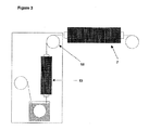
- FIGS 2 a and 2 b schematically embodiments of a dip-coating unit of the present invention are shown.
- the solution container 1 and the furnace 2 are arranged in a vertical set-up. Due to the vertical set-up no guide roller is required between the solution container 1 and the furnace 2.
- no guide roller is required between the solution container 1 and the furnace 2.
- pulling means For transportation of the substrate tape 4 pulling means are provided, which are usually arranged downstream to the furnace 2. For pulling a take-up roller 7 can be provided.
- the substrate tape 4 to the solution container 1 supply means can be provided, e. g. a pay-out roller 3.
- the dip-coating unit of the present invention can comprise a pre-drying zone 13 between coating container 1 and furnace 2.
- the pre-drying zone the freshly deposited green layer is pre-hardened at elevated temperature, however, yet not converted to the final material. Due to this pre-hardening step the risk of damage of the layer by mechanical impact is reduced which facilitates further processing. That is, when pre-hardened the risk of damage by contact with hard surfaces is essentially minimized. Consequently for further moving the substrate of long length e. g. to furnace 2 for final heat treatment, according to need, contact with surfaces such as of guide rollers 14 is now possible without the risk of damage.
- any suitable pre-drying means such as drying oven etc. can be used for the pre-drying zone.
- a barrier or similar means can be provided for closing the solution container 1 toward its environment.
- evaporated material of the coating solution is prevented to come into contact with the heater surface and the part of the substrate tape in the heated area of the heaters in the pre-drying zone 13 and/or furnace 2 which could cause undesired deposition of precursor fragments such as carbon etc.
- the coating solution can be contained in a tank which is closed towards its environment. Further, it is also possible to house the solution container 1 in a housing shielding the solution container 1 towards the furnace 2.
- any other constructional means suitable to prevent evaporated precursor solution to reach the heated area of the furnace and pre-drying zone, respectively, is likewise applicable.
- over-pressure can be applied to the space outside the barrier separating the solution container for avoiding entering of any evaporated material.
- FIG 4 A further embodiment of a dip-coating unit of the present invention is shown in figure 4 wherein the solution container 1 is designed as a coating nozzle 8.
- the coating nozzle 8 has a vertical slit 9 in its interior which extends from the bottom to the top of the nozzle 8 for passage of the substrate tape 4. That is, in this embodiment the substrate tape 4 is passed through the coating nozzle in vertical manner, too.
- the slit 9 at least comprises two parts of different width arranged one after the other in vertical manner with a lower part 10 having a width which is only some microns larger than the thickness of the substrate tape 4 and an upper part 11 with a larger width containing the coating solution. As shown in figure 4 the substrate tape 4 to be coated is fed via the lower slit part 10 and passed through the upper part 11 with the coating solution.
- a supply pipe 12 Connected to the upper slit part 11 is a supply pipe 12 for supplying the coating solution.
- coating solution can be continuously supplied to the upper slit part 11. Since the volume of the coating solution within the upper slit part 11 can be only small the exchange rate can be high. For example, in the production of coated conductors the volume in the upper slit part 11 can be selected generally to be 1 ml or less resulting in an exchange rate of only a few hours.
- the dimensions of the lower and upper slit part 10 and 11 generally depend on the dimensions of the substrate tape 4 such as thickness, width etc..
- the upper slit part 11 in case of a substrate tape 4 with 10 mm width it would be sufficient to design the upper slit part 11 to be about 20 mm in height and 5 mm and 12 mm, respectively, in the lateral directions.
- the width of the lower slit part 10 is usually selected such to just allow the passage of the tape. That is, usually the width is only marginally wider than the width or cross-sectional extension of the substrate. Thus, depending on the surface tension of the coating solution leakage of the coating solution from the upper slit part 11 through the lower slit part 10 may be prevented by the surface tension of the coating solution itself.
- the lower slit part 10 should be made or lined with a material of low surface energy such as teflon, teflon coated steel etc..
- the supply pipe 12 is vertically connected to the upper slit part 11.
- the connection is not restricted to such vertical connection but can be carried out in any manner suitable for supply of the coating solution to the coating nozzle 8.
- FIGS 6 a and 6 b cross-sectional views of suitable architectures for double-sided coated conductors obtainable according to the present invention are shown.
- the double-sided coated conductors as shown in figure 6 a and 6 b comprise a substrate 15 and on each the front and rear side at least a buffer layer 16 and a superconductor layer 17.
- a second buffer layer 18 is comprised.
- Typical thickness for these layers in nowadays coated conductors are from about 25 ⁇ m to about 150 ⁇ m for the substrate, from about 50 nm to about 2500 nm for the buffer layers and from about 500 nm to about 5000 nm for the superconductor layers.
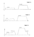
- Suitable temperature profiles for the pre-hardening step in pre-drying zone 13 and the final heat treatment are shown in figures 7 a, 7 b and 7 c with the vertical axis indicating the temperature.
- the temperature can be kept constant during the whole pre-drying and final heat treatment step.
- the temperature in the pre-drying step and the final heat treatment step can be varied over the heating time in different manners according to need and as is in principle generally known in the production of high temperature superconductor coated conductors.
- a suitable temperature for converting the freshly deposited layer to the final oxide material is usually selected from about 700 to 850°C. If the temperature is higher, for example about 900°C, due to the high reactivity of YBCO reaction with the buffer layer has been observed. Further, oxygen diffusion through the buffer layer can take place leading to undesired oxidation of the metal substrate.
- double-sided coated conductors can be obtained with a superconductor layer and/or one or more buffer layers provided on both sides of the substrate of long length by a non-vacuum deposition technique, such as MOD, simultaneously and in continuous manner, wherein the simultaneously deposited layers are defect free and of equally high quality.
- a non-vacuum deposition technique such as MOD
Landscapes
- Chemical & Material Sciences (AREA)
- Engineering & Computer Science (AREA)
- Materials Engineering (AREA)
- General Chemical & Material Sciences (AREA)
- Chemical Kinetics & Catalysis (AREA)
- Thermal Sciences (AREA)
- Physics & Mathematics (AREA)
- Mechanical Engineering (AREA)
- Metallurgy (AREA)
- Organic Chemistry (AREA)
- Inorganic Chemistry (AREA)
- Dispersion Chemistry (AREA)
- Ceramic Engineering (AREA)
- Manufacturing & Machinery (AREA)
- Superconductors And Manufacturing Methods Therefor (AREA)
Priority Applications (1)
| Application Number | Priority Date | Filing Date | Title |
|---|---|---|---|
| EP06300891A EP1892319A1 (fr) | 2006-08-24 | 2006-08-24 | Appareil pour le revêtement en continu de substrats allongés |
Applications Claiming Priority (1)
| Application Number | Priority Date | Filing Date | Title |
|---|---|---|---|
| EP06300891A EP1892319A1 (fr) | 2006-08-24 | 2006-08-24 | Appareil pour le revêtement en continu de substrats allongés |
Publications (1)
| Publication Number | Publication Date |
|---|---|
| EP1892319A1 true EP1892319A1 (fr) | 2008-02-27 |
Family
ID=37547725
Family Applications (1)
| Application Number | Title | Priority Date | Filing Date |
|---|---|---|---|
| EP06300891A Withdrawn EP1892319A1 (fr) | 2006-08-24 | 2006-08-24 | Appareil pour le revêtement en continu de substrats allongés |
Country Status (1)
| Country | Link |
|---|---|
| EP (1) | EP1892319A1 (fr) |
Cited By (3)
| Publication number | Priority date | Publication date | Assignee | Title |
|---|---|---|---|---|
| EP2472618A1 (fr) | 2011-01-03 | 2012-07-04 | Nexans | Limiteur de courant de défaut à superconduction |
| JP2014026847A (ja) * | 2012-07-27 | 2014-02-06 | Furukawa Electric Co Ltd:The | 超電導線の製造方法および製造装置 |
| WO2017138899A1 (fr) | 2016-02-12 | 2017-08-17 | Istanbul Teknik Universitesi Rektorlugu | Dispositif et procédé permettant un revêtement continu de fibres de carbone avec un procédé électrochimique |
Citations (8)
| Publication number | Priority date | Publication date | Assignee | Title |
|---|---|---|---|---|
| US2667429A (en) * | 1949-02-11 | 1954-01-26 | Rca Corp | Coating mixture with addition agent and method of coating therewith |
| US4753822A (en) * | 1985-10-18 | 1988-06-28 | U.S. Philips Corp. | Method of providing a bonding, electrically insulating layer, metal ribbon coated with such a layer, and low-loss magnet core |
| US4759949A (en) * | 1987-07-23 | 1988-07-26 | Westinghouse Electric Corp. | Method of insulating ferromagnetic amorphous metal continuous strip |
| EP0280292A2 (fr) * | 1987-02-26 | 1988-08-31 | Sumitomo Electric Industries Limited | Procédé de la fabrication d'une couche en matériau d'oxyde supraconducteur |
| EP0356352A2 (fr) * | 1988-08-25 | 1990-02-28 | EASTMAN KODAK COMPANY (a New Jersey corporation) | Articles conducteurs riches en Yttrium et leurs procédés de préparation |
| JPH0741375A (ja) * | 1993-07-30 | 1995-02-10 | Chichibu Onoda Cement Corp | ディップコーティング装置およびこのディップコーティング装置を用いたセラミックス薄膜の製膜方法 |
| US20030162667A1 (en) * | 2002-02-22 | 2003-08-28 | Amit Goyal | Powder-in-tube and thick-film methods of fabricating high temperature superconductors having enhanced biaxial texture |
| US6673387B1 (en) * | 2000-07-14 | 2004-01-06 | American Superconductor Corporation | Control of oxide layer reaction rates |
-
2006
- 2006-08-24 EP EP06300891A patent/EP1892319A1/fr not_active Withdrawn
Patent Citations (8)
| Publication number | Priority date | Publication date | Assignee | Title |
|---|---|---|---|---|
| US2667429A (en) * | 1949-02-11 | 1954-01-26 | Rca Corp | Coating mixture with addition agent and method of coating therewith |
| US4753822A (en) * | 1985-10-18 | 1988-06-28 | U.S. Philips Corp. | Method of providing a bonding, electrically insulating layer, metal ribbon coated with such a layer, and low-loss magnet core |
| EP0280292A2 (fr) * | 1987-02-26 | 1988-08-31 | Sumitomo Electric Industries Limited | Procédé de la fabrication d'une couche en matériau d'oxyde supraconducteur |
| US4759949A (en) * | 1987-07-23 | 1988-07-26 | Westinghouse Electric Corp. | Method of insulating ferromagnetic amorphous metal continuous strip |
| EP0356352A2 (fr) * | 1988-08-25 | 1990-02-28 | EASTMAN KODAK COMPANY (a New Jersey corporation) | Articles conducteurs riches en Yttrium et leurs procédés de préparation |
| JPH0741375A (ja) * | 1993-07-30 | 1995-02-10 | Chichibu Onoda Cement Corp | ディップコーティング装置およびこのディップコーティング装置を用いたセラミックス薄膜の製膜方法 |
| US6673387B1 (en) * | 2000-07-14 | 2004-01-06 | American Superconductor Corporation | Control of oxide layer reaction rates |
| US20030162667A1 (en) * | 2002-02-22 | 2003-08-28 | Amit Goyal | Powder-in-tube and thick-film methods of fabricating high temperature superconductors having enhanced biaxial texture |
Cited By (3)
| Publication number | Priority date | Publication date | Assignee | Title |
|---|---|---|---|---|
| EP2472618A1 (fr) | 2011-01-03 | 2012-07-04 | Nexans | Limiteur de courant de défaut à superconduction |
| JP2014026847A (ja) * | 2012-07-27 | 2014-02-06 | Furukawa Electric Co Ltd:The | 超電導線の製造方法および製造装置 |
| WO2017138899A1 (fr) | 2016-02-12 | 2017-08-17 | Istanbul Teknik Universitesi Rektorlugu | Dispositif et procédé permettant un revêtement continu de fibres de carbone avec un procédé électrochimique |
Similar Documents
| Publication | Publication Date | Title |
|---|---|---|
| EP1525627B1 (fr) | Procede et appareil permettant le depot d'un materiau supraconducteur sur un substrat en bande | |
| US6797313B2 (en) | Superconductor methods and reactors | |
| KR100683186B1 (ko) | 다층 제품 및 그의 제조방법 | |
| CN100502073C (zh) | 前体溶液及其使用方法 | |
| KR100997881B1 (ko) | 테이프 기판상의 초전도체 재료 | |
| CN1993497B (zh) | 用于制造高织构的带形高温超导体的方法 | |
| US20050065035A1 (en) | Superconductor methods and reactors | |
| Paranthaman et al. | Fabrication of Long Lengths of Epitaxial Buffer Layers on Biaxially Textured Nickel Substrates Using a Continuous Reel‐to‐Reel Dip‐Coating Unit | |
| US8268386B2 (en) | Method for manufacturing high-temperature superconducting conductors | |
| EP0476876A2 (fr) | Procédé pour le traitement thermique non-destructif d'un supraconducteur enroulé recouvert l'une couche d'argent à haute temperature | |
| Knoth et al. | Chemical solution deposition of YBa2Cu3O7− x coated conductors | |
| US20120318196A1 (en) | System for forming superconductor material on a tape substrate | |
| US7910155B2 (en) | Method for manufacturing high temperature superconducting conductor | |
| EP1892319A1 (fr) | Appareil pour le revêtement en continu de substrats allongés | |
| US20040020430A1 (en) | Method and apparatus for forming a thin film on a tape substrate | |
| KR100764527B1 (ko) | 적층막 및 성막방법 | |
| CN101599526A (zh) | 制备涂布导体用成形衬底的工艺及使用该衬底的涂布导体 | |
| Ono et al. | Crystal growth of YBa/sub 2/Cu/sub 3/O/sub 7-X/thin films prepared by TFA-MOD method | |
| JP2014216126A (ja) | テープ状酸化物超電導線材の製造方法及び積層仮焼成膜作製装置 |
Legal Events
| Date | Code | Title | Description |
|---|---|---|---|
| PUAI | Public reference made under article 153(3) epc to a published international application that has entered the european phase |
Free format text: ORIGINAL CODE: 0009012 |
|
| AK | Designated contracting states |
Kind code of ref document: A1 Designated state(s): AT BE BG CH CY CZ DE DK EE ES FI FR GB GR HU IE IS IT LI LT LU LV MC NL PL PT RO SE SI SK TR |
|
| AX | Request for extension of the european patent |
Extension state: AL BA HR MK YU |
|
| AKX | Designation fees paid | ||
| REG | Reference to a national code |
Ref country code: DE Ref legal event code: 8566 |
|
| STAA | Information on the status of an ep patent application or granted ep patent |
Free format text: STATUS: THE APPLICATION IS DEEMED TO BE WITHDRAWN |
|
| 18D | Application deemed to be withdrawn |
Effective date: 20080828 |