EP1892609A1 - Corps planaire transparent et commutateur tactile transparent - Google Patents
Corps planaire transparent et commutateur tactile transparent Download PDFInfo
- Publication number
- EP1892609A1 EP1892609A1 EP06746812A EP06746812A EP1892609A1 EP 1892609 A1 EP1892609 A1 EP 1892609A1 EP 06746812 A EP06746812 A EP 06746812A EP 06746812 A EP06746812 A EP 06746812A EP 1892609 A1 EP1892609 A1 EP 1892609A1
- Authority
- EP
- European Patent Office
- Prior art keywords
- transparent
- transparent conductive
- layer
- refractive index
- touch switch
- Prior art date
- Legal status (The legal status is an assumption and is not a legal conclusion. Google has not performed a legal analysis and makes no representation as to the accuracy of the status listed.)
- Withdrawn
Links
Images


Classifications
-
- H—ELECTRICITY
- H01—ELECTRIC ELEMENTS
- H01B—CABLES; CONDUCTORS; INSULATORS; SELECTION OF MATERIALS FOR THEIR CONDUCTIVE, INSULATING OR DIELECTRIC PROPERTIES
- H01B5/00—Non-insulated conductors or conductive bodies characterised by their form
- H01B5/14—Non-insulated conductors or conductive bodies characterised by their form comprising conductive layers or films on insulating-supports
-
- H—ELECTRICITY
- H01—ELECTRIC ELEMENTS
- H01H—ELECTRIC SWITCHES; RELAYS; SELECTORS; EMERGENCY PROTECTIVE DEVICES
- H01H13/00—Switches having rectilinearly-movable operating part or parts adapted for pushing or pulling in one direction only, e.g. push-button switch
- H01H13/70—Switches having rectilinearly-movable operating part or parts adapted for pushing or pulling in one direction only, e.g. push-button switch having a plurality of operating members associated with different sets of contacts, e.g. keyboard
- H01H13/83—Switches having rectilinearly-movable operating part or parts adapted for pushing or pulling in one direction only, e.g. push-button switch having a plurality of operating members associated with different sets of contacts, e.g. keyboard characterised by legends, e.g. Braille, liquid crystal displays, light emitting or optical elements
-
- G—PHYSICS
- G06—COMPUTING OR CALCULATING; COUNTING
- G06F—ELECTRIC DIGITAL DATA PROCESSING
- G06F3/00—Input arrangements for transferring data to be processed into a form capable of being handled by the computer; Output arrangements for transferring data from processing unit to output unit, e.g. interface arrangements
- G06F3/01—Input arrangements or combined input and output arrangements for interaction between user and computer
- G06F3/03—Arrangements for converting the position or the displacement of a member into a coded form
- G06F3/041—Digitisers, e.g. for touch screens or touch pads, characterised by the transducing means
- G06F3/044—Digitisers, e.g. for touch screens or touch pads, characterised by the transducing means by capacitive means
- G06F3/0445—Digitisers, e.g. for touch screens or touch pads, characterised by the transducing means by capacitive means using two or more layers of sensing electrodes, e.g. using two layers of electrodes separated by a dielectric layer
-
- G—PHYSICS
- G06—COMPUTING OR CALCULATING; COUNTING
- G06F—ELECTRIC DIGITAL DATA PROCESSING
- G06F3/00—Input arrangements for transferring data to be processed into a form capable of being handled by the computer; Output arrangements for transferring data from processing unit to output unit, e.g. interface arrangements
- G06F3/01—Input arrangements or combined input and output arrangements for interaction between user and computer
- G06F3/03—Arrangements for converting the position or the displacement of a member into a coded form
- G06F3/041—Digitisers, e.g. for touch screens or touch pads, characterised by the transducing means
- G06F3/044—Digitisers, e.g. for touch screens or touch pads, characterised by the transducing means by capacitive means
- G06F3/0446—Digitisers, e.g. for touch screens or touch pads, characterised by the transducing means by capacitive means using a grid-like structure of electrodes in at least two directions, e.g. using row and column electrodes
-
- G—PHYSICS
- G06—COMPUTING OR CALCULATING; COUNTING
- G06F—ELECTRIC DIGITAL DATA PROCESSING
- G06F3/00—Input arrangements for transferring data to be processed into a form capable of being handled by the computer; Output arrangements for transferring data from processing unit to output unit, e.g. interface arrangements
- G06F3/01—Input arrangements or combined input and output arrangements for interaction between user and computer
- G06F3/03—Arrangements for converting the position or the displacement of a member into a coded form
- G06F3/041—Digitisers, e.g. for touch screens or touch pads, characterised by the transducing means
- G06F3/044—Digitisers, e.g. for touch screens or touch pads, characterised by the transducing means by capacitive means
- G06F3/0448—Details of the electrode shape, e.g. for enhancing the detection of touches, for generating specific electric field shapes, for enhancing display quality
-
- G—PHYSICS
- G06—COMPUTING OR CALCULATING; COUNTING
- G06F—ELECTRIC DIGITAL DATA PROCESSING
- G06F3/00—Input arrangements for transferring data to be processed into a form capable of being handled by the computer; Output arrangements for transferring data from processing unit to output unit, e.g. interface arrangements
- G06F3/01—Input arrangements or combined input and output arrangements for interaction between user and computer
- G06F3/03—Arrangements for converting the position or the displacement of a member into a coded form
- G06F3/041—Digitisers, e.g. for touch screens or touch pads, characterised by the transducing means
- G06F3/045—Digitisers, e.g. for touch screens or touch pads, characterised by the transducing means using resistive elements, e.g. a single continuous surface or two parallel surfaces put in contact
-
- H—ELECTRICITY
- H03—ELECTRONIC CIRCUITRY
- H03K—PULSE TECHNIQUE
- H03K17/00—Electronic switching or gating, i.e. not by contact-making and –breaking
- H03K17/94—Electronic switching or gating, i.e. not by contact-making and –breaking characterised by the way in which the control signals are generated
- H03K17/96—Touch switches
- H03K17/962—Capacitive touch switches
-
- H—ELECTRICITY
- H03—ELECTRONIC CIRCUITRY
- H03K—PULSE TECHNIQUE
- H03K17/00—Electronic switching or gating, i.e. not by contact-making and –breaking
- H03K17/94—Electronic switching or gating, i.e. not by contact-making and –breaking characterised by the way in which the control signals are generated
- H03K17/96—Touch switches
- H03K17/9645—Resistive touch switches
-
- G—PHYSICS
- G06—COMPUTING OR CALCULATING; COUNTING
- G06F—ELECTRIC DIGITAL DATA PROCESSING
- G06F2203/00—Indexing scheme relating to G06F3/00 - G06F3/048
- G06F2203/041—Indexing scheme relating to G06F3/041 - G06F3/045
- G06F2203/04103—Manufacturing, i.e. details related to manufacturing processes specially suited for touch sensitive devices
-
- G—PHYSICS
- G06—COMPUTING OR CALCULATING; COUNTING
- G06F—ELECTRIC DIGITAL DATA PROCESSING
- G06F3/00—Input arrangements for transferring data to be processed into a form capable of being handled by the computer; Output arrangements for transferring data from processing unit to output unit, e.g. interface arrangements
- G06F3/01—Input arrangements or combined input and output arrangements for interaction between user and computer
- G06F3/03—Arrangements for converting the position or the displacement of a member into a coded form
- G06F3/041—Digitisers, e.g. for touch screens or touch pads, characterised by the transducing means
- G06F3/0412—Digitisers structurally integrated in a display
-
- Y—GENERAL TAGGING OF NEW TECHNOLOGICAL DEVELOPMENTS; GENERAL TAGGING OF CROSS-SECTIONAL TECHNOLOGIES SPANNING OVER SEVERAL SECTIONS OF THE IPC; TECHNICAL SUBJECTS COVERED BY FORMER USPC CROSS-REFERENCE ART COLLECTIONS [XRACs] AND DIGESTS
- Y10—TECHNICAL SUBJECTS COVERED BY FORMER USPC
- Y10T—TECHNICAL SUBJECTS COVERED BY FORMER US CLASSIFICATION
- Y10T428/00—Stock material or miscellaneous articles
- Y10T428/24—Structurally defined web or sheet [e.g., overall dimension, etc.]
- Y10T428/24802—Discontinuous or differential coating, impregnation or bond [e.g., artwork, printing, retouched photograph, etc.]
Definitions
- the present invention relates to a transparent planar body and a transparent touch switch.
- Patent Document 1 discloses a transparent touch switch comprising a dielectric layer lying between a pair of transparent planar bodies each provided with a transparent conductive film patterned into a predetermined shape.
- the transparent touch switch detects the touched position by sensing the change of electric capacity via grounding through a human body.
- Such a transparent touch switch is mounted on the surface of a liquid crystal display apparatus, CRT or the like.
- the shape of the pattern of the transparent electric conduction film that is formed in the transparent planar body becomes conspicuous, lowering visibility of the touch switch.
- a transparent conductive film disclosed in Patent Document 2 is one example of the known transparent planar body.
- the transparent conductive film comprises an undercoat layer between a conductive-layer formation film and a conductive layer.
- the undercoat layer is formed from two layers having different refractive indices. Specifically, a highly refractive zinc oxide/tin oxide film having a thickness of 600 ⁇ is disposed near the conductive-layer formation film and a lower refractive silicon oxide film having a thickness of 450 ⁇ is disposed near the conductive layer.
- this transparent conductive film When this transparent conductive film is used as a transparent electrostatic capacitive touch switch, the pattern shape of the conductive layer also becomes conspicuous, and therefore there is room for improvement in this respect.
- An object of the present invention is to provide a transparent planar body and a transparent touch switch that have improved visibility.
- the object of the present invention can be achieved by a transparent planar body comprising a transparent substrate; a patterned transparent conductive film formed on at least one surface of the transparent substrate; and a transmittance-adjusting layer for equalizing the transmission spectrum of light that is transmitted through a patterned region where the transparent conductive film is provided via the transparent substrate with that transmitted through a non-patterned region where the transparent conductive film is not provided.
- the transmittance-adjusting layer be provided with an overcoat layer covering one surface of the transparent substrate with a substantially uniform thickness, and the overcoat layer be thicker than the transparent conductive film and have a lower refractive index than the transparent conductive film.
- the overcoat layer be formed of a silicon-tin oxide.
- the overcoat layer have a thickness of 70 to 80 nm.
- the difference in refractive index between the transparent conductive film and the overcoat layer be 0.03 to 0.4.
- a preferable structure is achieved when an undercoat layer lies between the transparent substrate and the transparent conductive film, wherein the undercoat layer is formed from a laminate comprising at least two layers having different light refractive indices, and the transparent conductive film is formed on the low refractive index layer side.
- the object of the present invention can be achieved with a transparent touch switch comprising a plurality of transparent planar bodies, wherein the plurality of transparent planar bodies are attached to each other via an adhesive layer and function as a transparent electrostatic capacitive touch switch, and the refractive index of the adhesive layer is less than that of the transparent conductive film.
- a linear polarizing plate be provided on the front side.
- the transparent touch switch comprise a linear polarizing plate and a quarter-wave plate on the front side and a quarter-wave plate on the back side.
- the transparent substrate be a quarter-wave plate.
- the transmittance-adjusting layer be provided with an undercoat layer formed from a laminate comprising a low refractive index layer and a high refractive index layer whose light refractive index is higher than that of the low refractive index layer, wherein the undercoat layer lies between the transparent substrate and the transparent conductive film in such a manner that the transparent conductive film is formed on the low refractive index layer side, and the high refractive index layer is thinner than the low refractive index layer.
- the high refractive index layer have a thickness of 10 to 25 nm and the low refractive index layer have a thickness of 25 to 45 nm.
- the high refractive index layer be formed of a silicon-tin oxide and the low refractive index layer be formed of a silicon oxide.
- the transparent conductive film have a thickness of 10 to 25 nm
- the object of the present invention can be achieved by a transparent electrostatic capacitive touch switch comprising a plurality of transparent planar bodies attached to each other via an adhesive layer.
- the object of the present invention can also be achieved by a transparent electrostatic capacitive touch switch comprising a plurality of transparent planar bodies, wherein each of the plurality of transparent planar bodies is disposed in such a manner that the transparent conductive films thereof face each other and the plurality of transparent planar bodies are attached to each other having an adhesive layer therebetween.
- the thickness of the transparent conductive film is 20 to 25 nm, and the refractive index of the adhesive layer is not less than 1.6.
- a transparent electrostatic capacitive touch switch comprising a plurality of transparent planar bodies, wherein each of the plurality of transparent planar bodies is disposed in such a manner that the transparent conductive films thereof face each other and the plurality of transparent planar bodies are attached to each other having an adhesive layer therebetween, wherein the thickness of the transparent conductive film is 25 to 30 nm, and the refractive index of the adhesive layer is not less than 1.7.
- a linear polarizing plate be provided on the front side.
- Such transparent touch switch be provided with a linear polarizing plate and a quarter-wave plate on the front side and a quarter-wave plate on the back side.
- the transparent substrate be a quarter-wave plate.
- the transmittance-adjusting layer comprise a cover layer to cover an exposed portion where the transparent conductive film is not formed on one surface of the transparent substrate, wherein the cover layer be formed so that the surface thereof is flush with the surface of the transparent conductive film, and the refractive index of the cover layer be the substantially same as that of the transparent conductive film.
- the cover layer be formed of a silicon-tin oxide.
- the transparent conductive film be formed of a carbon nanotube composite material.
- the transparent planar body further comprise an undercoat layer that is formed of a laminate of a low refractive index layer and a high refractive index layer having a light refractive index higher than that of the low refractive index layer, wherein the undercoat layer lies between the transparent conductive film and the cover layer and the transparent substrate, i.e., the undercoat layer lies on the transparent conductive film and under the cover layer and the transparent substrate, so that the transparent conductive film and the cover layer are disposed on the low refractive index layer side.
- the transparent planar body further comprise an overcoat layer covering the surfaces of the transparent conductive film and the cover layer, wherein the overcoat layer has a flat surface.
- the object of the present invention can also be achieved by the transparent electrostatic capacitive touch switch comprising a plurality of transparent planar bodies, wherein the plurality of transparent planar bodies are attached to each other via an adhesive layer.
- the object of the present invention can also be achieved by a transparent resistive film-type touch switch comprising a plurality of transparent planar bodies arranged in such a manner that the transparent conductive films face each other and the transparent planar bodies have a predetermined space therebetween via a spacer.
- a linear polarizing plate be provided on the front side.
- a linear polarizing plate and a quarter-wave plate be provided on the front side and a quarter-wave plate be provided on the back side.
- the transparent substrate be a quarter-wave plate.
- the transparent conductive film comprise a plurality of belt-like transparent conductive members disposed with a predetermined space therebetween
- the transmittance-adjusting layer comprise a belt-like transparent controlling member disposed between two belt-like transparent conductive members via an insulating slit in between
- the belt-like transparent controlling member be formed of the same material as that of the belt-like transparent conductive member and comprise a plurality of resistive slits.
- the plurality of resistive slits be arranged so as to connect one insulating slit to another those adjacent to each belt-like transparent controlling members.
- a transparent planar body further comprise a separating slit disposed along the insulating slit so as to separate each belt-like transparent controlling member.
- the object of the present invention can be achieved by a transparent electrostatic capacitive touch switch comprising a plurality of transparent planar bodies, wherein each transparent planar body is attached to each other via an adhesive layer.
- the object of the present invention can be achieved by a transparent resistive film-type touch switch comprising a plurality of transparent planar bodies, wherein the plurality of transparent planar bodies are arranged so as to have a predetermined space therebetween produced by a spacer so that the belt-like transparent electric conductors face each other.
- Such a transparent touch switch comprise a linear polarizing plate on the front side.
- a linear polarizing plate and a quarter-wave plate be provided on the front side and a quarter-wave plate be provided on the back side.
- the transparent substrate be a quarter-wave plate.
- the present invention provides a transparent planar body and a transparent touch switch that can improve visibility.
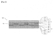
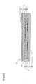
- FIG. 1 is a schematic cross-sectional view showing the transparent touch switch of the first embodiment of the present invention.
- the transparent touch switch 101 is an electrostatic capacitive touch switch comprising a first transparent planar body 1 wherein a transparent conductive film 12 is formed on a transparent substrate 11 via an undercoat layer 13, and a second transparent planar body 2 wherein a transparent conductive film 22 is formed on a transparent substrate 21 via an undercoat layer 23.
- the first transparent planar body 1 and the second transparent planar body 2 are attached to each other via an adhesive layer 15 in such a manner that the transparent conductive films 12 and 22 face each other.
- the transparent substrates 11 and 21 are structured so that hard-coat layers 112,112 and 212,212 are formed on the front and back surfaces of base material layers 111 and 211 respectively. It is preferable that the base material layers 111 and 211 be formed of a highly transparent material.
- preferable materials include polyethylene terephthalate (PET), polyethylene naphthalate (PEN), polyether sulfone (PES), polyether ether ketone (PEEK), polycarbonate (PC), polypropylene (PP), polyamide (PA), polyacrylic acid (PAC), epoxy resins, phenol resins, aliphatic cyclic polyolefins, transparent norbornene-based thermoplastic resins and like flexible films; laminates of two or more such resins; glass plates; etc.
- the thickness of the base material layers 111 and 211 is preferably about 20 to 500 ⁇ m, and the thickness of the hard-coat layers 112 and 212 is preferably about 3 to 5 ⁇ m. In order to increase the rigidity, a support may be attached to the base material layers 111 and 211.
- the undercoat layers 13 and 23 are formed from a laminate of two or more layers having different light refractive indices, wherein the layer having a lower refractive index is formed on the side of the transparent conductive films 12 and 22 respectively in order to increase the transparency.
- Examples of materials for the laminate of undercoat layers 13 and 23 include silicon oxide, titanium oxide, tin oxide, etc. Examples of preferable combinations include tin oxide/hafnium oxide, silicon oxide/tin oxide, zinc oxide/tin oxide, tin oxide/titanium oxide, etc.
- the undercoat layers 13 and 23 can be formed by sputtering, vacuum evaporation, electron beam evaporation, etc.
- Examples of materials for the transparent conductive films 12 and 22 include indium tin oxide (ITO), zinc oxide, indium oxide, antimony-doped tin oxide, fluorine-doped tin oxide, aluminum-doped zinc oxide, potassium-doped zinc oxide, silicon-doped zinc oxide, zinc oxide/tin oxide, indium oxide/tin oxide, zinc oxide/indium oxide/magnesium oxide and like metal oxides. These materials may be used in combination.
- Examples of methods for forming transparent conductive films 12 and 22 include sputtering, vacuum deposition, ion plating and like PVD methods; CVD methods; coating methods; printing methods; etc.
- the thickness of the transparent conductive films 12 and 22 is generally about 10 to 50 nm.
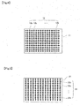
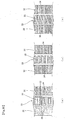
- Each of the transparent conductive films 12 and 22 is formed, as shown in Figs. 2 and 3 , as an assembly of plurality of belt-like conductive members 12a and 22a extending in parallel.
- the belt-like conductive members 12a and 22a of the transparent conductive films 12 and 22 are disposed so as to perpendicularly intersect each other.
- the transparent conductive films 12 and 22 are connected to an outside drive circuit (not shown) via a routed circuit (not shown) formed of conductive ink, etc.
- the pattern of the transparent conductive films 12 and 22 is not limited to that in the present embodiment, and various patterns may be employed as long as the point touched with a finger, etc., can be detected. For example, as shown in Figs.
- the transparent conductive films 12 and 22 may have a structure, wherein a plurality of diamond-shaped conductive members 12b and 22b are linearly connected, the directions in which the diamond-shaped conductive members 12b and 22b are connected in each of the transparent conductive films 12 and 22 intersect at right angles, and the diamond-shaped conductive members 12b and 22b do not overlap each other as seen in a plan view.
- the patterning of the transparent conductive films 12 and 22 can be conducted in the following manner. First, a mask having a predetermined shape is formed on the surfaces of the transparent conductive films 12 and 22, those disposed on the transparent substrates 11 and 21 via the undercoat layers 13 and 23 respectively. Second, the exposed portions are removed by etching using an acid liquid, etc., and the mask is then dissolved using an alkaline liquid, etc. By employing a method wherein the transparent conductive films 12 and 22 are patterned into a predetermined shape by etching, unnecessary transparent conductive films 12 and 22 can be removed while retaining the entire undercoat layers 13 and 23. However, the patterning method is not limited to this and other known methods may be employed. The undercoat layers 13 and 23 may be removed together with the unnecessary transparent conductive films 12 and 22.
- the first transparent planar body 1 and the second transparent planar body 2 in the transparent touch switch of the present embodiment comprise overcoat layers 14 and 24 on the opposing surfaces (the surfaces on which transparent conductive films 12 and 22 are formed).
- the preferable materials for the overcoat layers 14 and 24 include silicon oxide, titanium oxide, tin oxide, etc. A particularly preferable material is silicon-tin oxide.
- the thickness of the overcoat layers 14 and 24 is generally about 10 to 500 nm and the refractive index is generally about 1.3 to 2.3.
- the overcoat layer 14 in the first transparent planar body 1 be thicker than the transparent conductive film 12 and have a refractive index smaller than that of the transparent conductive film 12.
- the overcoat layer 24 of the second transparent planar body 2 it is preferable that the overcoat layer 24 have a thickness greater than that of the transparent conductive film 22 and a refractive index smaller than that of the transparent conductive film 22.
- the refractive index of the overcoat layer 14 can be suitably controlled by, for example, if the overcoat layer is formed of a silicon-tin oxide, changing the ratio between silicon and tin.
- the shapes of the transmission and reflection spectra from the first transparent planar body 1 and the second transparent planar body 2 can be equalized in the portions where the transparent conductive films 12 and 22 are formed and not formed, so that the difference in tones (light to dark) can be reduced.
- patterns of the transparent conductive films 12 and 22 in the first transparent planar body 1 and the second transparent planar body 2 become inconspicuous, improving visibility.
- the overcoat layers 14 and 24 become thicker, the shape of the transmission spectrum (or the reflection spectrum) in the portions without transparent conductive films 12 and 22 gradually equalizes to that in the portions where the transparent conductive films 12 and 22 are provided. Therefore, by suitably selecting the thickness of the overcoat layers 14 and 24 so that the shapes of the spectra become substantially coincident in both portions, i.e., with and without the transparent conductive films 12 and 22, excellent visibility can be attained.
- the overcoat layers 14 and 24 are formed of a silicon-tin oxide (having a refractive index of about 1.7), it is preferable that the overcoat layers 14 and 24 have a thickness of 70 to 80 nm as shown in the Experimental Examples described later.
- the refractive index of the overcoat layers 14 and 24 be smaller than that of the transparent conductive films 12 and 22.
- the difference in the refractive index is preferably 0.03 to 0.4, and more preferably 0.1 to 0.3.
- Examples of methods for forming the overcoat layers 14 and 24 include sputtering, vacuum evaporation, electron beam evaporation and like dry coating methods. Such method makes it possible to form the overcoat layers 14 and 24 having a uniform thickness on the exposed surfaces of the undercoat layers 13 and 23 and the surfaces of the transparent conductive films 12 and 22 of the first transparent planar body 1 and the second transparent planar body 2.
- Attachment between the first transparent planar body 1 and the second transparent planar body 2 is preferably conducted in such a manner that an adhesive layer 15 lies between the entire attached surfaces so as to prevent formation of an air layer.
- Epoxy-based, acryl-based and like generally used transparent adhesives may be used as the adhesive layer 15, and they may include a core material formed from a transparent film of norbornene-based resin.
- the thickness of the adhesive layer 15 is generally 25 to 75 ⁇ m, and the refractive index is generally 1.4 to 1.6.
- the refractive index of the adhesive layer 15 be smaller than that of the overcoat layers 14 and 24.
- Such arrangement makes the refractive indices of the transparent conductive film 12 (or 22), the overcoat layer 14 (or 24) and the adhesive layer 15 gradually become smaller in this order (i.e., in the order in which they are laminated. This makes it possible to equalize the shapes of the transmission spectrum and reflection spectrum in the entire transparent touch switch between the portions the transparent conductive films 12 and 22 are provided and not provided, reducing the difference in tones (light to dark). This makes the patterns of the transparent conductive films 12 and 22 in the first transparent planar body 1 and the second transparent planar body 2 inconspicuous and improves visibility.
- the method for detecting the touched position is the same as that in known electrostatic capacitive touch switches. Specifically, when the front surface of the first transparent planar body 1 is touched with a finger at any point, the transparent conductive films 12 and 22 are grounded through the electric capacity of a human body in the touched position. By detecting the current value which flows through the transparent electric conduction films 12 and 22 at this time, the coordinate of the touched position can be calculated. It is preferable that the surface resistance value of the overcoat layers 14 and 24 be large enough to obtain satisfactory insulation properties as an electrostatic capacitive touch switch, for example, not less than 1 x 10 12 ( ⁇ / ⁇ ).
- a linear polarizing plate may be provided on the front side (that is opposite to the surface on which the transparent conductive film 12 is formed) of the first transparent planar body 1.
- the transparent substrates 11 and 21 should be formed of an optical isotropic material.
- a linear polarizing plate is an oriented film of polyvinyl alcohol (PVA) to which iodine, dichromatic dye or like dichromatic coloring matter is adsorbed and oriented.
- the linear polarizing plate may be formed by attaching a triacetyl acetate (TAC) film that functions as a protective film in such a manner that the thus-obtained oriented film is sandwiched between the triacetyl acetate (TAC) films.
- TAC triacetyl acetate
- Optical isotropic materials are those that have no polarization to any incidental light, for example, polycarbonate (PC), polyether sulfone (PES), polyacrylic acid (PAC), amorphous polyolefin resin, cyclic polyolefin resins, aliphatic cyclic polyolefins, norbornene thermoplastic transparent resins, glass materials, etc. Examples of the methods for forming the transparent substrates 11 and 21 using these materials include casting and extrusion.
- Such an arrangement can reduce the amount of reflected light attributable to the visible light incident in the touch switch by half or less compared to the case when a linear polarizing plate is not provided.
- This arrangement also makes the transparent conductive films 12 and 22 more inconspicuous and improves visibility of the touch switch.
- the quarter-wave plate may be formed by extending a film formed of polyvinyl alcohol (PVA), polycarbonate (PC), norbornene thermoplastic resin, cyclic polyolefin resin or the like to impart multiple flexibilities. It is preferable that the linear polarizing plate be fully attached to the quarter-wave plate having an adhesive layer formed of the materials usable for the adhesive layer 15 in between in such a manner that the formation of an air layer is prevented.
- PVA polyvinyl alcohol
- PC polycarbonate
- norbornene thermoplastic resin cyclic polyolefin resin or the like to impart multiple flexibilities.
- the linear polarizing plate be fully attached to the quarter-wave plate having an adhesive layer formed of the materials usable for the adhesive layer 15 in between in such a manner that the formation of an air layer is prevented.
- the quarter-wave plate be attached to the second transparent planar body on the back side with an adhesive layer formed of the materials usable for the adhesive layer 15 lying in between so as to prevent formation of an air layer.
- the quarter-wave plates be arranged in such a manner that the optical axis of one quarter-wave plate perpendicularly intersects with the axis of the other quarter-wave plate.
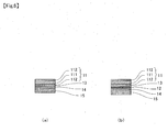
- Sample A shown in Fig. 6 (a) was a laminate wherein a transparent substrate 11, an undercoat layer 13, an overcoat layer 14, and an adhesive layer 15 are laminated in this order without providing a transparent conductive film.
- the transparent substrate 11 was formed in such a manner that two hard-coat layers 112 and 112 having a thickness of 3 to 5 ⁇ m was formed on the front and back surfaces of a base material layer 111 formed from a 200 ⁇ m thick PET film.
- the undercoat layer 13 was formed in such a manner that a silicon oxide layer having a thickness of 30 nm and a silicon-tin oxide layer having a thickness of 70 nm were layered on the transparent substrate 11 in this order.
- the adhesive layer 15 was formed from an acrylic adhesive (P043FP product of Lintec Corporation) so as to have a thickness of 20 to 30 ⁇ m.
- Sample B shown in Fig. 6(b) was formed in such a manner that a transparent conductive film 12 having a thickness of 30 nm formed of ITO was provided between the undercoat layer 13 and the overcoat layer 14 of Sample A shown in Fig. 6(a) .
- the transparent conductive film 12 had a refractive index of 1.95.
- Transmission spectra of Samples A and B were measured from the front surface of the transparent substrate 11.
- a spectrophotometer U-3310, product of Hitachi, Ltd.
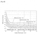
- Fig. 7(a) transmission spectra of Samples A and B were similar in both portions.
- the thickness of the overcoat layer 14 was set at 70 nm as described above, and irradiation was conducted using a 24 W three band fluorescent lamp while varying the irradiation angle. The shape of the electric conduction pattern was barely observed, and satisfactory results were obtained.
- Samples C and D were prepared in such a manner that the overcoat layer 14 was not provided in the structures of Samples A and B shown in Figs. 6(a) and 6(b) .
- the transmission spectra of Samples C and D were measured in the same manner as in the Example described above. As shown in Fig. 8 , there was a large difference in the shapes of the transmission spectra especially at low wavelengths.
- FIG. 9 is a schematic cross-sectional view showing the transparent touch switch according to the second embodiment of the present invention.
- the transparent touch switch 101 is an electrostatic capacitive touch switch, which comprises a first transparent planar body 1 formed by providing a transparent conductive film 12 on a transparent substrate 11 via an undercoat layer 13; and a second transparent planar body 2 formed by providing a transparent conductive film 22 on a transparent substrate 21 via an undercoat layer 23.
- the first transparent planar body 1 and the second transparent planar body 2 are attached to each other via the adhesive layer 15 in such a manner that the transparent conductive films 12 and 22 face each other.
- the transparent substrates 11 and 21 are formed by providing hard-coat layers 112,112 and 212,212 on the front and back surfaces of the base material layers 111 and 211. It is preferable that the base material layers 111 and 211 be formed of a highly transparent material.
- the thickness of the base material layers 111 and 211 be about 20 to 500 ⁇ m, and the thickness of the hard-coat layers 112 and 212 be about 3 to 5 ⁇ m.
- a support may be provided.
- the hard-coat layers 112 and 212 be provided on the front and back surfaces of the base material layers 111 and 211.
- the undercoat layers 13 and 23 are formed from laminates of low refractive index layers 13a and 23a and high refractive index layers 13b and 23b having a higher light refractive index than the low refractive index layers 13a and 23a.
- the transparent conductive films 12 and 22 are formed on the low refractive index layers 13a and 23a side so as to improve transparency.
- Examples of the materials for the layers that form laminates for the undercoat layers 13 and 23 include silicon oxide, titanium oxide, tin oxide, etc.
- the undercoat layers 13 and 23 can be formed by sputtering, vacuum evaporation, electron beam evaporation, etc.
- the high refractive index layers 13b and 23b be thinner than the low refractive index layers 13a and 23a.
- Such arrangement can make the shapes of the patterns of the transparent conductive films 12 and 22 formed on the surfaces of the undercoat layers 13 and 23 inconspicuous and improve visibility of the touch switch.
- the thickness of the high refractive index layers 13b and 23b be 10 to 25 nm.
- the thickness of the low refractive index layers 13a and 23a be 25 to 45 nm.
- Examples of the materials for the transparent conductive films 12 and 22 include indium tin oxide (ITO), zinc oxide, indium oxide, antimony-doped tin oxide, fluorine-doped tin oxide, aluminum-doped zinc oxide, potassium-doped zinc oxide, silicon-doped zinc oxide, zinc oxide/tin oxide, indium oxide/tin oxide, zinc oxide/indium oxide/magnesium oxide and like metal oxides. These materials may be used in combination.
- the transparent conductive films 12 and 22 can be formed by sputtering, vacuum deposition, ion plating and like PVD methods; CVD methods; coating methods; printing methods; etc.
- the transparent conductive films 12 and 22 are formed, as in the first embodiment, as an assembly of a plurality of belt-like conductive members 12a and 22a respectively, extending in parallel as shown in Figs. 2 and 3 .
- the belt-like conductive members 12a and 22a of the transparent conductive films 12 and 22 are disposed so as to perpendicularly intersect to each other.
- the transparent conductive films 12 and 22 are connected to an outside drive circuit (not shown) via a routed circuit (not shown) formed of conductive ink, etc.
- the pattern of the transparent conductive films 12 and 22 is not limited to that in the present embodiment, and various patterns may be employed as long as the position touched with a finger, etc., can be detected. For example, as shown in Figs.
- the transparent conductive films 12 and 22 may have the following structure.
- a plurality of diamond-shaped conductive members 12b and 22b are linearly connected, wherein the connection directions of the diamond-shaped conductive members 12b and 22b in the transparent conductive films 12 and 22 intersect at right angles, and the diamond-shaped conductive members 12b and 22b do not overlap each other as seen in a plan view.
- Patterning of the transparent conductive films 12 and 22 can be conducted in the following manner. First, a mask having a predetermined shape is formed on the surface of the transparent conductive films 12 and 22 those disposed on the transparent substrates 11 and 21 via the undercoat layers 13 and 23. Second, the exposed portions are removed by etching using an acid liquid, etc., and then the mask is resolved using an alkaline liquid, etc. By employing the method wherein the transparent conductive films 12 and 22 are patterned into a predetermined shape by etching, unnecessary transparent conductive films 12 and 22 can be removed while retaining the entire undercoat layers 13 and 23. However, the pattering method is not limited to this and other known methods may be employed.
- the thickness of the transparent conductive films 12 and 22 be generally about 10 to 50 nm. In order to make the shapes of the patterns of the transparent conductive films 12 and 22 inconspicuous and improve visibility, it is preferable that the transparent conductive films 12 and 22 be made as thin as possible. However, if the transparent conductive films 12 and 22 are too thin, it becomes difficult to obtain excellent crystallizability and satisfactory durability and weathering resistance of the film, and therefore the preferable thickness is about 10 to 25 nm.
- Attachment between the first transparent planar body 1 and the second transparent planar body 2 is preferably conducted in such a manner that an adhesive layer 15 lies on the entire attached surfaces so as to prevent formation of an air layer.
- the adhesive layer 15 may be formed of epoxy-based, acryl-based and like generally used transparent adhesives, and may include a core material formed from a transparent film of norbornene-based resin.
- the adhesive layer 15 generally has a thickness of 25 to 75 ⁇ m, and a refractive index of 1.4 to 1.6.
- the transparent substrates 11 and 21 are formed by providing a hard-coat layer (thickness: 5 ⁇ m, refractive index: 1.52) on the front and back surfaces of a base material layer (thickness: 188 ⁇ m, refractive index: 1.65) formed from a PET film.
- a high refractive index layer is formed from a silicon-tin oxide film (thickness: 25 nm, refractive index: 1.7) and a low refractive index layer is formed from a silicon oxide film (thickness: 30 nm, refractive index: 1.43).
- the transparent conductive films 12 and 22 are formed from an ITO film (thickness: 30 nm, refractive index: 1.95).
- the thickness of the adhesive layer 15 is 25 ⁇ m, and the refractive index of the adhesive layer 15 is varied as a parameter.
- the difference in the reflectance (%) between the portions where the transparent conductive films 12 and 22 are formed and the portions where the transparent conductive films 12 and 22 are not formed (i.e., the portions where the cover layers 16 and 26 are formed) was calculated based on the simulation.
- the reflectance was calculated using a thin film designing software (Optas-Film available from Cybernet Systems Co., Ltd.).
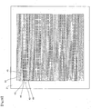
- Figure 10 shows the absolute values of the differences in reflectance (%) obtained using this simulation.
- calculation of reflectance was conducted assuming the thicknesses of the transparent substrates 11 and 21, the adhesive layer 15, etc., which are very large compared to the thickness of the undercoat layers 13 and 23, the transparent conductive films 12 and 22 and like components having a nano-order thickness, to be ⁇ (infinite).
- the inconspicuousness of the pattern shapes of the transparent conductive films 12 and 22 is correlated to the degree of the difference in reflectance between the portions where the transparent conductive films 12 and 22 are formed and not formed.
- the absolute values of the reflectance difference becomes smaller as the refractive index of the adhesive layer 15 becomes greater. Therefore, making the refractive index of the adhesive layer 15 greater is preferable from the viewpoint of visibility.
- the difference in the reflectance (%) between the portions where the transparent conductive films 12 and 22 are formed and not formed were simulated while varying the refractive index of the adhesive layer 15 as a parameter.
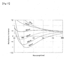
- Figures 11 to 13 show the simulation results. Note that Fig. 11 shows the results when the thickness of the transparent conductive films 12 and 22 is 15 nm, Fig. 12 shows the results when the thickness is 20 nm, and Fig. 13 shows the results when the thickness is 25 nm.
- Table 1 shows the absolute values of the reflectance difference extracted from the simulation results shown in Figs. 10 to 13 at specific refractive indices of adhesive layer 15 with the input light wavelength of 550 nm.
- Table 1 Refractive Indices of Adhesive Layer 15 Thickness of Transparent Conductive Film 15 nm 20 nm 25 nm 30 nm 1.52 0.20 0.48 0.74 0. 98 1. 60 0.15 0.37 0.58 0.76 1. 65 0.13 0.31 0.48 0.63 1.70 0.10 0.24 0.39 0.51 1.75 0.07 0.19 0.30 0.39 1.80 0.05 0.13 0.21 0.29
- the absolute value of the reflectance difference can be made less than about 0.5 by using an adhesive layer 15 having a refractive index of not less than 1.6. Therefore, by setting the thickness of the transparent conductive films 12 and 22 within the range of 20 to 25 nm and using an adhesive layer 15 having a refractive index of not less than 1.6 in the transparent touch switch 101 having the structure as shown in Fig. 9 , a transparent touch switch 101 having excellent visibility wherein the pattern shapes of the transparent conductive films 12 and 22 are inconspicuous can be obtained.
- the method for detecting the touched position is the same as that in known electrostatic capacitive touch switches. Specifically, the front surface of the first transparent planar body 1 is touched with a finger, etc., at any point, the transparent conductive films 12 and 22 are grounded through the electric capacity of a human body in the touched position. By detecting the current value which flows through the transparent electric conduction films 12 and 22 at this time, the coordinate of the touched position can be calculated.
- a linear polarizing plate may be provided on the front side (the surface opposite to that on which the transparent conductive film 12 is formed) of the first transparent planar body 1.
- the transparent substrates 11 and 21 should be formed of an optical isotropic material.
- the usable materials for the linear polarizing plate include polyvinyl alcohol (PVA) oriented films in which iodine, dichroic dye or like dichroic coloring matter is adsorbed and oriented.
- the linear polarizing,plate may be formed by attaching a triacetyl acetate (TAC) film that functions as a protective film in such a manner that the thus-obtained oriented film is sandwiched between the triacetyl acetate (TAC) films.
- TAC triacetyl acetate
- Optical isotropic materials are those that do not show polarizing characteristics to any incidental light, such as polycarbonate (PC), polyether sulfone (PES), polyacrylic acid (PAC), amorphous polyolefin resins, cyclic polyolefin resins, aliphatic cyclic polyolefins, norbornene thermoplastic transparent resins, glass materials, etc.
- the transparent substrates 11 and 21 can be formed by casting or extruding these materials.
- This structure can reduce the amount of reflected light attributable to visible light entering the touch switch to about less than half of that when the polarizing plate is not provided. Furthermore, this arrangement makes' the transparent conductive films 12 and 22 more inconspicuous and improves visibility.
- the quarter-wave plate may be formed by extending a film formed of polyvinyl alcohol (PVA), polycarbonate (PC), norbornene thermoplastic resin, cyclic polyolefin resin or the like to impart multiple flexibilities. It is preferable that the linear polarizing plate be fully attached with the quarter-wave plate having an adhesive layer formed of the materials usable for the adhesive layer 15 in between, in such a manner that the formation of an air layer is prevented.
- PVA polyvinyl alcohol
- PC polycarbonate
- norbornene thermoplastic resin cyclic polyolefin resin or the like to impart multiple flexibilities.
- the linear polarizing plate be fully attached with the quarter-wave plate having an adhesive layer formed of the materials usable for the adhesive layer 15 in between, in such a manner that the formation of an air layer is prevented.
- the quarter-wave plate be attached to the second transparent planar body on the back side with an adhesive layer formed of the materials usable for the adhesive layer 15 lying in between so as to prevent formation of an air layer.
- the quarter-wave plates be arranged in such a manner that the optical axis of one quarter-wave plate perpendicularly intersects with the axis of the other quarter-wave plate.
- the present invention is applied to a transparent electrostatic capacitive touch switch wherein two transparent planar bodies are attached via an adhesive layer.
- the difference in reflectance (%) between the portion where the transparent conductive film is formed and the portion where the transparent conductive film is not formed was obtained by simulation.
- the transparent substrate is obtained by providing a hard-coat layer (thickness: 5 ⁇ m, refractive index: 1.52) on the front and back surfaces of a base material layer (thickness: 188 ⁇ m, refractive index: 1.65) that is formed from a PET film.
- the transparent conductive film is formed from an ITO film (refractive index: 1.95).
- an adhesive layer (thickness: 25 ⁇ m, refractive index: 1.52) formed of an acrylic resin was formed.
- the reflectance was calculated using a thin film designing software (Optas-Film available from Cybernet Systems Co., Ltd.). In this calculation, absorption in the PET layer, etc., was disregarded.
- Figure 14 shows the reflectance (%) differences obtained by using the thickness of the transparent conductive film as a parameter in this structure.
- the inconspicuousness of the pattern shape of the transparent conductive film is correlative to the reflectance difference between the portions where the transparent conductive film is formed and not formed.
- the absolute values of the reflectance difference becomes smaller as the transparent conductive film becomes thinner, and therefore making the transparent conductive film thinner is preferable from the viewpoint of visibility.
- a certain thickness is necessary, and therefore the thickness of the transparent conductive film is preferably 10 to 25 nm, and the optimally about 15 nm.
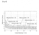
- the optimum thicknesses of a low refractive index layer and a high refractive index layer forming the undercoat layer in the structure (shown in Fig. 9 ) wherein an undercoat layer is formed between a transparent substrate and a transparent conductive film were determined.
- the thickness and refractive index of the transparent substrate and the refractive index of the transparent conductive film were assumed to be the same as those in Experimental Example 1, and the thickness of the transparent conductive film was determined to be 15 nm based on the results of Experimental Example 1.
- An adhesive layer was formed on the front side of the transparent conductive film, wherein the thickness and refractive index of the adhesive layer were also made to be the same as those in Experimental Example 1.
- the undercoat layer was formed as a laminate of a low refractive index layer formed of silicon oxide having a refractive index of 1.43 and a high refractive index layer formed of a silicon-tin oxide having a refractive index of 1.7.
- the thickness of the low refractive index layer was set at 30 nm, the thickness of the high refractive index layer was varied as a parameter, and then the reflectance difference between the portions where the transparent conductive film is formed and not formed was obtained by simulation.
- Figure 15 shows the results.
- the thickness of the high refractive index layer was 0 (i.e., the high refractive index layer was not present), the absolute values and rate of change of reflectance difference in the low-wave length side (about 400 to 500 nm) of the visible region became greater, and this made it difficult to obtain excellent visibility.
- the thickness of the high refractive index layer was 10 to 20 nm, the absolute values and rate of change of the reflectance difference were small in the entire visible region, and excellent visibility was obtained.
- the thickness of the high refractive index layer became larger than 30 nm, which was the thickness of the low refractive index layer, the absolute values and rate of change of the reflectance difference tended to increase again and this tended to reduce visibility.
- the thickness of the high refractive index layer in the undercoat layer is preferably smaller than that of the low refractive index layer. More specifically, the thickness of the high refractive index layer is preferably 10 to 25 nm and, in this case, the thickness of the low refractive index layer is preferably 25 to 45 nm.
- the preferred thicknesses of the low refractive index layer and the high refractive index layer in the undercoat layer obtained in Experimental Example 2 have almost the same tendency even when the thickness of layers other than the undercoat layer changes.
- the transparent conductive film in Experimental Example 2 becomes thicker, there is almost no change in the ranges of the preferred thickness of the low refractive index layer and the high refractive index layer, but visibility remarkably decreases when the thicknesses do not fall within these preferred ranges.
- Figure 17 shows the reflectance differences when the thickness of the transparent conductive film was changed from 15 to 20 nm in the structure of Experimental Example 2 (the thickness of the low refractive index layer: 30 nm) with using the thickness of the high refractive index layer as a parameter.
- the ranges of the preferred thickness of the high refractive index layer and the low refractive index layer in the undercoat layer tend to be widened compared to that of Experimental Example 2.
- a certain degree of visibility can be obtained even when an undercoat layer is formed from only a low refractive index layer without providing a high refractive index layer.
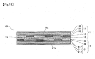
- FIG. 18 is a schematic cross-sectional view illustrating the transparent touch switch according to the third embodiment of the present invention.
- This transparent touch switch 101 is an electrostatic capacitive touch switch comprising a first transparent planar body 1 having a patterned transparent conductive film 12 formed on one surface of a transparent substrate 11, and a second transparent planar body 2 having a patterned transparent conductive film 22 formed on one surface of a transparent substrate 21.
- the first transparent planar body 1 and the second transparent planar body 2 are attached to each other via an adhesive layer 15 in such a manner that the transparent conductive films 12 and 22 face each other.
- the transparent substrates 11 and 21 are structured so that hard-coat layers 112,112 and 212,212 are formed on the front and back surfaces of base material layers 111 and 211 respectively. It is preferable that the base material layers 111 and 211 be formed of a highly transparent material.
- preferable materials include polyethylene terephthalate (PET), polyethylene naphthalate (PEN), polyether sulfone (PES), polyether ether ketone (PEEK), polycarbonate (PC), polypropylene (PP), polyamide (PA), polyacrylic acid (PAC), epoxy resins, phenol resins, aliphatic cyclic polyolefins, transparent norbornene-based thermoplastic resins and like flexible films; laminates of two or more such resins; glass plates; etc.
- the thickness of the base material layers 111 and 211 is preferably about 20 to 500 ⁇ m, and the thickness of the hard-coat layers 112 and 212 is preferably about 3 to 5 ⁇ m. In order to increase the rigidity, a support may be attached to the base material layers 111 and 211.
- Examples of materials for the transparent conductive films 12 and 22 include indium tin oxide (ITO), indium oxide, antimony-doped tin oxide, fluorine-doped tin oxide, aluminum-doped zinc oxide, potassium-doped zinc oxide, silicon-doped zinc oxide, zinc oxide/tin oxide, indium oxide/tin oxide, zinc oxide/indium oxide/magnesium oxide, zinc oxide and like metal oxides. These materials may be used alone or in combination.
- ITO indium tin oxide
- indium oxide antimony-doped tin oxide
- fluorine-doped tin oxide aluminum-doped zinc oxide
- potassium-doped zinc oxide silicon-doped zinc oxide
- zinc oxide/tin oxide indium oxide/tin oxide
- zinc oxide/indium oxide/magnesium oxide zinc oxide and like metal oxides.
- composite materials wherein carbon nanotubes, carbon nanohorns, carbon nanowires, carbon nanofibers, graphite fibril and like superthin electric conduction carbon fibers are disposed in a polymer material, which functions as a binder, as materials for the transparent conductive films 12 and 22.
- a polymer material which functions as a binder, as materials for the transparent conductive films 12 and 22.
- usable polymer materials include polyaniline, polypyrrole, polyacetylene, polythiophene, polyphenylene vinylene, polyphenylene sulfide, poly (p-phenylene) poly(heterocyclic vinylene), poly(3,4-ethylenedioxythiophene) (PEDOT) and like conductive polymers.
- non-conductive polymers such as polyethylene terephthalate (PET), polyethylene naphthalate (PEN), polyether sulfone (PES), polyether ether ketone (PEEK), polycarbonate (PC), polypropylene (PP), polyamide (PA), polyacrylic acid (PAC), polyimide, epoxy resins, phenol resins, aliphatic cyclic polyolefins, norbornene thermoplastic transparent resins and like non-conductive polymers.
- PET polyethylene terephthalate
- PEN polyethylene naphthalate
- PES polyether sulfone
- PEEK polyether ether ketone
- PC polypropylene
- PA polyamide
- PA polyacrylic acid
- polyimide polyimide
- epoxy resins phenol resins, aliphatic cyclic polyolefins, norbornene thermoplastic transparent resins and like non-conductive polymers.
- a carbon nanotube composite material obtained by dispersing carbon nanotubes in a non-conductive polymer material is used as a material for the transparent conductive films 12 and 22, because carbon nanotubes are extremely thin with a diameter of generally about 0.8 to 1.4 nm (i.e., around 1 nm), by dispersing the carbon nanotube in the non-conductive polymer material one-by-one or one-bundle-by-one-bundle, blockage of light transmittance due to the carbon nanotubes can be reduced. This is preferable so as to reliably obtain transparency of the transparent conductive films 12 and 22.
- Examples of the methods for forming the transparent conductive films 12 and 22 include sputtering, vacuum deposition, ion plating and like PVD methods; CVD methods; coating methods; printing methods; etc.
- the thickness of the transparent conductive films 12 and 22 is generally about 10 to 50 nm.
- Each of the transparent conductive films 12 and 22 is formed, as shown in Figs. 2 and 3 , as an assembly of pluralities of belt-like conductive members 12a and 22a extending in parallel.
- the belt-like conductive members 12a and 22a of the transparent conductive films 12 and 22 are disposed so as to perpendicularly intersect to each other.
- the transparent conductive films 12 and 22 are connected to an outside drive circuit (not shown) via a routed circuit (not shown) formed of conductive ink, etc.
- the pattern of the transparent conductive films 12 and 22 is not limited to that in the present embodiment, and various patterns may be employed as long as the point touched with a finger, etc., can be detected. For example, as shown in Figs.
- the transparent conductive films 12 and 22 may have a structure, wherein a plurality of diamond-shaped conductive members 12b and 22b are linearly connected, the directions in which the diamond-shaped conductive members 12b and 22b are connected in each of the transparent conductive films 12 and 22 intersect at right angles, and the diamond-shaped conductive members 12b and 22b do not overlap each other as seen in a plan view.
- Patterning of the transparent conductive films 12 and 22 can be conducted by forming a mask having a predetermined shape on the surface of the transparent conductive films 12 and 22 formed on the transparent substrates 11 and 21, removing the exposed portions by etching using an acid liquid, etc., and then dissolving the mask using an alkaline liquid, etc.
- the patterning method is not limited to this and any known method may be employed.
- cover layers 16 and 26 are formed so as to cover the exposed portions 11a and 21a.
- the cover layers 16 and 26 are formed so that the surfaces thereof become substantially flush with the surfaces of the transparent conductive films 12 and 22.
- Examples of the materials for the cover layers 16 and 26 include silicon-tin oxide, silicon oxide, titanium oxide, tin oxide, cerium oxide, niobium pentoxide, tantalum pentoxide, zirconium oxide; zirconium oxide/silicon oxide, zirconium oxide/tin oxide, zirconium oxide/titanium dioxide and like composite oxides; etc.
- silicon-tin oxide is preferable.
- the refractive index of the cover layers 16 and 26 is equivalent to that of the transparent conductive films 12 and 22 and can be suitably controlled by, for example, if the cover layers are formed of a silicon-tin oxide, changing the ratio between silicon and tin.
- the "refractive index of the cover layers 16 and 26 is equivalent to that of the transparent conductive films 12 and 22" means not only that the refractive index of the cover layers 16 and 26 is completely coincident with that of the transparent conductive films 12 and 22, but also includes the case when there is a difference in the refractive index between the cover layers 16 and 26 and the transparent conductive films 12 and 22 to such an extent that the pattern shape of the transparent conductive films 12 and 22 can be made inconspicuous.
- the absolute values of the difference in the refractive indices between the cover layers 16 and 26 and the transparent conductive films 12 and 22 is preferably not more than 0.08, and more preferably not more than 0.03.
- a carbon nanotube composite material is selected as a material for the transparent conductive films 12 and 22, because the refractive index of the carbon nanotube composite material is lower than that of indium tin oxide (ITO), i.e., the refractive index of a carbon nanotube composite material is about 1.6 and the refractive index of an indium tin oxide is about 1.9 to 2.0, selection of the materials for the cover layers 16 and 26 having a refractive index equivalent to that of the transparent conductive films 12 and 22 becomes easy.
- ITO indium tin oxide
- the shape and the refractive index of the cover layers 16 and 26 as described above, it is possible to make the shape of the transmission spectrum and reflection spectrum of the first transparent planar body 1 and the second transparent planar body 2 substantially the same in the portions where the transparent conductive films 12 and 22 are formed and not formed, reducing the difference in tones (light to dark).
- the pattern shape in the transparent conductive films 12 and 22 can be made inconspicuous, and visibility can be improved.
- Examples of the methods for forming the cover layers 16 and 26 include sputtering, vacuum evaporation, electron beam evaporation and like dry coating methods. A specific method for forming the cover layers 16 and 26 using such dry coating method is explained below.
- a mask 50 having a desirable pattern shape is formed on the surface of the transparent substrate 11 (21) of the transparent conductive film 12 (22).
- the exposed portion 51 of the transparent conductive film 12 (22) on which the mask 50 is not formed is removed by etching to form exposed portion 11a (21a) ( Fig. 19(b) ).
- the material for the cover layer is applied to the exposed portion 11a (21a) and on top of the mask 50 by a dry coating method.
- the thickness of the cover layer formed on the exposed portion 11a (21a) is made substantially the same as that of the transparent conductive film 12 (22) ( Fig. 19(c) ). Subsequently, by removing the mask 50, the cover layer 16 (26) that is substantially flush with the transparent conductive film 12 (22) can be formed on the exposed portion 11a (21a) ( Fig. 19(d) ).
- etching is conducted so as to make the surface of the cover layers 16 and 26 on the first transparent planar body 1 and the second transparent planar body 2 flush with the surface of the transparent conductive films 12 and 22.
- Attachment between the first transparent planar body 1 and the second transparent planar body 2 is preferably conducted in such a manner that an adhesive layer 15 lies on the entire attachment surface so that formation of an air layer can be prevented.
- the adhesive layer 15 may be formed of epoxy-based, acryl-based and like generally used transparent adhesives, and may include a core material formed from a transparent film of norbornene-based resin.
- the thickness of the adhesive layer 15 is generally 25 to 100 ⁇ m.
- the method for detecting the touched position is the same as that in known electrostatic capacitive touch switches. Specifically, the front surface of the first transparent planar body 1 is touched with a finger or the like at any point, the transparent conductive films 12 and 22 are grounded through the electric capacity of a human body in the touched position. By detecting the current value which flows through the transparent electric conduction films 12 and 22 at this time, the coordinate of the touched position can be calculated. It is preferable that the surface resistance value of the overcoat layers 14 and 24 be large enough to obtain satisfactory insulation properties as an electrostatic capacitive touch switch, for example, not less than 1 x 10 12 ( ⁇ / ⁇ ).
- the overcoat layers 14 and 24 may be provided to cover the surfaces of the transparent conductive films 12 and 22 and the cover layers 16 and 26.
- the overcoat layers 14 and 24 are formed so as to have entirely flat surfaces 14a and 24a.
- the surface resistance value of the overcoat layers 14 and 24 be large enough to obtain satisfactory insulating properties so that it can properly operate as an electrostatic capacitive touch switch, for example, not less than 1 x 10 12 ( ⁇ / ⁇ ).
- Examples of the methods for forming the overcoat layers 14 and 24 include sputtering, vacuum evaporation, electron beam evaporation and like dry coating methods; and screen printing, photogravure printing, barcoating, spin coating, die coating, spray coating and like wet coating methods.
- overcoat layers 14 and 24 When a material for the overcoat layers 14 and 24 is the same as, for example, that for the cover layers 16 and 26, it is possible to simultaneously form the cover layers 16 and 26 and the overcoat layers 14 and 24 by screen printing, etc. This allows the formation of the transparent planar bodies 1 and 2 in an efficient manner. It is also possible to form the overcoat layers 14 and 24 using a material different from that of the cover layers 16 and 26.
- the thickness of the overcoat layers 14 and 24 is preferably from about 10 nm, which is the minimum film thickness feasible in the case of sputtered thin film, to about 30 nm, or not less than 1 ⁇ m.
- the details of the simulation are explained below.
- the transparent substrates 11 and 21 were obtained by forming a hard-coat layer (having a thickness of 5 ⁇ m and refractive index of 1.52) on the front and back surfaces of the base material layer (thickness: 188 ⁇ m, refractive index: 1.65) formed of a PET film.
- the transparent conductive films 12 and 22 were formed from an ITO film (thickness: 30 nm, refractive index: 1.95).
- the cover layers 16 and 26 were formed of a silicon-tin oxide (thickness: 30 nm, refractive index: 1.95).
- the adhesive layer 15 was formed of an acrylic resin (thickness: 25 ⁇ m, refractive index: 1.52).
- the refractive index of the overcoat layers was 1.9 and the thickness of the overcoat layers was varied as a parameter.
- the difference in the reflectance (%) between the portions where the transparent conductive films 12 and 22 are formed and portions where the transparent conductive films 12 and 22 are not formed (i.e., the portions where the cover layers 16 and 26 are formed) were simulated while varying this parameter.
- the reflectance was calculated using a thin film designing software (Optas-Film- available from Cybernet Systems Co., Ltd.).
- Figures 21 and 22 show the differences of reflectance (%) obtained by this simulation.
- Figure 21 shows the case when the thickness of the overcoat layers 14 and 24 was assumed as being of a nano order
- Fig. 22 shows the case when the thickness thereof was assumed as being of a ⁇ m order.
- the inconspicuousness of the pattern shape of the transparent conductive film is correlative to the reflectance difference between the portions where the transparent conductive film is formed and not formed.
- the absolute value of the reflectance difference is smaller than about 0.5, the pattern shape becomes more inconspicuous.
- the overcoat layers 14 and 24 be thinner than 30 nm so as to obtain excellent visibility.
- Fig. 22 which shows the results when the overcoat layers 14 and 24 have a nano-order thickness
- the absolute value of the reflectance difference is as small as about 0.5, and preferable from the viewpoint of visibility.
- the transparent electrostatic capacitive touch switch 101 has a structure wherein the first transparent planar body 1 and the second transparent planar body 2 are attached to each other via the adhesive layer 15 in such a manner that the transparent conductive films 12 and 22 face each other.
- it is also possible to obtain a transparent resistive film-type touch switch by arranging the first transparent planar body 1 and the second transparent planar body 2 in such a manner that the transparent conductive films 12 and 22 face each other having a predetermined space therebetween created by a spacer.
- the method for detecting the touched position is the same as that in known electrostatic capacitive touch switches. Specifically, the front surface of the first transparent planar body 1 is touched with a finger or the like at any point, the transparent conductive films 12 and 22. are grounded through the electric capacity of a human body in the touched position. By measuring the resistance at the touched point in a time-sharing manner in the vertical and horizontal directions, the coordinate of the touched position can be calculated.
- the transparent touch switch of the present embodiment may further comprise undercoat layers 13 and 23 formed from a laminate of a low refractive index layer and a high refractive index layer, whose light refractive index is higher than that of the low refractive index layer.
- the undercoat layers 13 and 23 lie between the transparent conductive films 12, 22 and the cover layers 16,26, and the transparent substrates 11, 21, i.e., the undercoat layers are disposed below the transparent conductive films and the cover layers but over the transparent substrates, so that the transparent conductive films 12 and 22 and the cover layers 16 and 26 are formed on the low refractive index layer side. This structure improves the transparency of the transparent touch switch 101.
- Examples of the materials for each layer of the laminate forming the undercoat layers 13 and 23 include silicon-tin oxide film, silicon oxide, titanium oxide, tin oxide, etc. Examples of preferable combinations include tin oxide/hafnium oxide, silicon oxide/tin oxide, zinc oxide/tin oxide, tin oxide/titanium oxide, etc.
- the undercoat layers 13 and 23 can be formed by sputtering, vacuum evaporation, electron beam evaporation, etc.
- the transparent touch switch 101 of the third embodiment it is also possible to provide a linear polarizing plate on the front side of the first transparent planar body 1 (the surface opposite to the surface on which the transparent conductive film 12 is formed).
- a linear polarizing plate it is necessary to form the transparent substrates 11 and 21 from an optical isotropic material.
- the materials for the linear polarizing plate include polyvinyl alcohol (PVA) oriented films in which iodine, dichroic dye or like dichroic coloring matter is adsorbed and oriented. It is also possible to attach a protective film of triacetyl acetate (TAC) on the surfaces of this film so as to hold it.
- PVA polyvinyl alcohol
- TAC triacetyl acetate
- Optical isotropic materials are those that do not show polarizing characteristics to any incidental light, such as polycarbonate (PC), polyether sulfone (PES), polyacrylic acid (PAC), amorphous polyolefin resins, cyclic polyolefin resins, aliphatic cyclic polyolefins, norbornene thermoplastic transparent resins, glass materials, etc.
- the transparent substrates 11 and 21 can be formed by casting or extruding these materials.
- Such an arrangement can reduce, the amount of reflected light attributable to visible light incident in the touch switch to about half compared to the case when the linear polarizing plate is not provided.
- This arrangement also makes the transparent conductive films 12 and 22 more inconspicuous and improves visibility.
- the quarter-wave plate may be formed by extending a film formed of polyvinyl alcohol (PVA), polycarbonate (PC), norbornene thermoplastic resin, cyclic polyolefin resin or the like to impart multiple flexibilities. It is preferable that the linear polarizing plate be fully attached, with the quarter-wave plate having an adhesive layer formed of the materials usable for the adhesive layer 15 in between in such a manner that the formation of an air layer is prevented.
- PVA polyvinyl alcohol
- PC polycarbonate
- norbornene thermoplastic resin cyclic polyolefin resin or the like to impart multiple flexibilities.
- the linear polarizing plate be fully attached, with the quarter-wave plate having an adhesive layer formed of the materials usable for the adhesive layer 15 in between in such a manner that the formation of an air layer is prevented.
- the quarter-wave plate be attached to the second transparent planar body on the back side, with an adhesive layer formed of the materials usable for the adhesive layer 15 lying in between, so as to prevent formation of an air layer.
- the quarter-wave plates be arranged in such a manner that the optical axis of one quarter-wave plate perpendicularly intersects with the axis of the other quarter-wave plate.
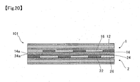
- FIG. 24 is a schematic cross-sectional view illustrating the touch switch according to the fourth embodiment of the present invention.
- the transparent touch switch 101 is an electrostatic capacitive touch switch comprising a first transparent planar body 1. having a plurality of belt-like transparent conductive members 32 disposed on one surface of the transparent substrate 11 with a predetermined space therebetween, and a second transparent planar body 2 having a plurality of belt-like transparent conductive members 42 disposed on one surface of the transparent substrate 21 with a predetermined space therebetween.
- the first transparent planar body 1 and the second transparent planar body 2 are attached to each other via the adhesive layer 15 in such a manner that the belt-like transparent conductive members 32 and 42 face each other.
- the transparent substrates 11 and 21 be formed of a highly transparent material.
- preferable materials include polyethylene terephthalate (PET), polyimide (PI), polyethylene naphthalate (PEN), polyether sulfone (PES), polyether ether ketone (PEEK), polycarbonate (PC), polypropylene (PP), polyamide (PA), polyacrylic acid (PAC), acrylic resins, amorphous polyolefin resins, cyclic polyolefin resins, aliphatic cyclic polyolefins, transparent norbornene-based thermoplastic resins and like flexible films;' laminates of two or more such resins; soda-lime glass, alkali free glass, borosilicate glass, quartz glass and like glass plates; etc.
- the thickness of the transparent substrates 11 and 21 is preferably about 20 to 500 ⁇ m. If the surface of the touch switch is to be touched by a pen, finger or the like, a hardcoat processing may be conducted on one or both surfaces of the transparent substrates 11 and 21 to improve the transparency, resistance to scuffing, wear resistance, non-glare properties, etc.
- a support may be attached to the transparent substrates 11 and 21 to increase the rigidity thereof.
- the materials for the support include glass plates, and resin materials having a hardness similar to that of glass.
- the thickness of the support is preferably not less than 100 ⁇ m and more preferably 0.2 to 0.5 mm.
- the first and second transparent planar bodies 1 and 2 comprise a plurality of belt-like transparent conductive members 32 and 42 formed on one surface of the transparent substrates 11 and 21 with a specific space therebetween.
- the first and second transparent planar bodies 1 and 2 further comprise belt-like transparent controlling members 33 and 43 formed of the same material as that of the belt-like transparent conductive members 32 and 42, disposed between each of the belt-like transparent conductive members 32 and 42 respectively.
- the belt-like transparent controlling members 33 and 43 formed of the same material as that of the belt-like transparent conductive members 32 and 42 are disposed between each belt-like transparent conductive members 32 and 42 respectively, the shape of the belt-like transparent conductive members 32 and 42 can be made inconspicuous, improving visibility.
- the belt-like transparent conductive members 32 and 42 and the belt-like transparent controlling members 33 and 43 have a rectangular shape, and they are alternately arranged side by side in a noncontact manner having insulating slits 34 and 44 from which the transparent substrates 11 and 21 are exposed in between.
- the belt-like transparent conductive members 32 and 42 are connected to an outside drive circuit (not shown) via a routed circuit (not shown) formed of conductive ink, etc., so that a voltage is applied thereto.
- the belt-like transparent conductive member 32 (belt-like transparent controlling member 33) of the first transparent planar body 1 and the belt-like transparent conductive member 42 (belt-like transparent controlling member 43) of the second transparent planar body 2 are disposed so as to intersect at right angles.
- the belt-like transparent controlling members 33 and 43 comprise a plurality of resistive slits 35 and 45, which extend in the direction along which the belt-like transparent conductive members 32 and 42 and the belt-like transparent controlling members 33 and 43 are in adjacent, and the plurality of resistive slits 35 and 45 connect the adjacent insulating slits 34 and 44.
- the belt-like transparent controlling members 33 and 43 comprise separating slits 36 and 46 respectively to separate the belt-like transparent controlling members 33 and 43 along the insulating slits 34 and 44.
- the shape of the belt-like transparent conductive members 32 and 42 is not limited to that of the present embodiment and they may have any shape as long as the point touched with a finger, etc., can be detected.
- the belt-like transparent conductive members 32 and 42 may have a structure, wherein a plurality of diamond-shaped conductive members are linearly connected in such a manner that their connecting directions in the belt-like transparent conductive members 32 and 42 intersect perpendicularly, and the diamond-shaped conductive members do not overlap each other as seen in a plan view.
- the area without the belt-like transparent conductive members 32 and 42 be made as small as possible when the first transparent planar body 1 and the second transparent planar body 2 are overlapped. From this point of view, a structure wherein a plurality of diamond-shaped conductive members are linearly connected is more preferable than rectangularly forming the belt-like transparent conductive members 32 and 42.
- FIGS. 27 and 28 show a structure wherein the belt-like transparent controlling members 33 and 43 are not provided with the separating slits 36 and 46.
- Examples of the materials for the belt-like transparent conductive members 32 and 42 and the belt-like transparent controlling members 33 and 43 include indium tin oxide (ITO), indium oxide, antimony-doped tin oxide, fluorine-doped tin oxide, aluminum-doped zinc oxide, potassium-doped zinc oxide, silicon-doped zinc oxide; zinc oxide-tin oxide, indium oxide-tin oxide, zinc oxide-indium oxide-magnesium oxide, zinc oxide, tin-oxide film and like transparent conductive materials; tin, copper, aluminum, nickel, chromium and like metal materials; and metal oxide materials.' These materials may be used alone or in combination. Simple metals that are weak to acids or alkalis may also be used as a conductive material.
- ITO indium tin oxide
- ITO indium oxide
- antimony-doped tin oxide fluorine-doped tin oxide
- aluminum-doped zinc oxide potassium-doped zinc oxide
- Zinc oxide (ZnO) is preferable for the material for the belt-like transparent conductive members 32 and 42 and the belt-like transparent controlling members 33 and 43, because it is less expensive than ITO, which is the most widely used material for touch switches, transparent electric conductors for liquid crystals, etc.
- ITO the most widely used material for touch switches, transparent electric conductors for liquid crystals, etc.
- zinc oxide is used as a material for the electrostatic capacitive touch switch
- the adhesive layer 15 lies between the first transparent planar body 1 and the second transparent planar body 2 without any air layer
- the belt-like transparent conductive members 32 and 42 and the belt-like transparent controlling members 33 and 43 formed of zinc oxide (ZnO) will not directly contact air. This prevents the zinc oxide (ZnO) from deteriorating due to oxidation and reduces the production costs of products (touch switch).
- composite materials wherein carbon nanotubes, carbon nanohorns, carbon nanowires, carbon nanofibers, graphite fibril and like superthin electric conduction carbon fibers are disposed in a polymer material, which functions as a binder, as materials for the belt-like transparent conductive members 32 and 42 and the belt-like transparent controlling members 33 and 43. It is also possible to provide an undercoat layer on the surface of the transparent substrates 11 and 21 to enhance the transparency and adherence thereof before forming the belt-like transparent conductive members 32 and 42 and the belt-like transparent controlling members 33 and 43.
- a conductive film having a uniform thickness is formed on one surface of the transparent substrates 11 and 21 using the above-described materials.
- the method for forming the conductive film include sputtering, vacuum deposition, ion plating and like PVD methods; CVD methods; coating methods; printing methods; etc.
- the thickness of the conductive film is generally about 5 to 100 nm
- the transparent substrates 11 and 21 or the laser light are moved so as to remove the conductive film. Separation between the belt-like transparent conductive members 32 and 42 and the belt-like transparent controlling members 33 and 43 is thereby conducted. The portions where the conductive film is removed by the irradiation of laser light become insulating slits 34 and 44.
- the apparatus for use in laser light irradiation include a YAG laser, a carbon laser, etc.
- the insulating slits 34 and 44 for separating the belt-like transparent conductive members 32 and 42 from the belt-like transparent controlling members 33 and 43 are formed using laser light as described above, it is possible to make the width of the insulating slits 34 and 44, for example, from 5 to 400 ⁇ m. This makes the boundaries between the belt-like transparent conductive members 32 and 42 and the belt-like transparent controlling members 33 and 43 inconspicuous, improving visibility. In particular, by making the width of the insulating slits 34 and 44 not more than 20 ⁇ m, the insulating slits 34 and 44 can be hardly recognized by visual observation. Therefore, it is preferable from the viewpoint of improving visibility.
- the resistive slits 35 and 45 and the separating slits 36 and 46 are formed as slits having a width of 5 to 400 ⁇ m by irradiating the surfaces of the belt-like transparent controlling members 33, and 43 with laser light so as to remove the conductive film.
- the widths of the resistive slits 35 and 45 and the separating slits 36 and 46 be not more than 20 ⁇ m.
- resistive slits 35 and 45 and the separating slits 36 and 46 be formed to divide the belt-like transparent controlling members 33 and 43 into small portions.
- resistive slits each having a width of 5 ⁇ m are formed in the belt-like transparent controlling members 33 and 43, having a length of 60581.8 ⁇ m and a width of 4880 ⁇ m in such a manner that the resistive slits have a space of 5 ⁇ m therebetween, 6058 resistive slits can be formed at the maximum.
- the width of the resistive slit be 9 ⁇ m and 9 to 3366 resistive slits be formed.
- a separating slit having a width of 5 ⁇ m is formed in the belt-like transparent controlling members 33 and 43 having the same size as described above, 486 separating slits can be formed at the maximum. It is preferable that the width of the separating slit be 9 ⁇ m and 0 to 269 separating slits be formed.
- the belt-like transparent controlling members 33 and 43 can be divided into 2,949,759 regions at the maximum. It is preferable that the belt-like transparent controlling members 33 and 43 be divided into 8 to 908,550 regions.
- Attachment between the first transparent planar body 1 and the second transparent planar body 2 is preferably conducted in such a manner that an adhesive layer 15 lies on the entire attachment surface so as to avoid formation of an air layer.
- the adhesive layer 15 may be formed of epoxy-based, acryl-based and like generally used transparent adhesive, and may include a core material formed from a transparent film of norbornene-based resin.
- the thickness of the adhesive layer 15 is preferably not more than 500 ⁇ m, more preferably 20 to 80 ⁇ m, and still more preferably 50 to 80 ⁇ m.
- the adhesive layer may be formed by layering a plurality of sheets of a single type of sheet-like adhesive material or a plurality of types of sheet-like adhesive materials.
- the method for detecting the position touched is the same as that in known electrostatic capacitive touch switches. Specifically, the front surface of the first transparent planar body 1 is touched with a finger or the like at any point, the transparent conductive films 12 and 22 are grounded through the electric capacity of a human body in the touched position. By detecting the current value which flows through the transparent electric conduction films 12 and 22 at this time, the coordinate of the touched position can be calculated.
- the belt-like transparent controlling members 33 and 43 comprise a plurality of resistive slits 35 and 45, and therefore when the front surface of the first transparent planar body 1 is touched, capacitive coupling occurs between the belt-like transparent conductive members 32 and 42 and the belt-like transparent controlling members 33 and 43, which are disposed adjacent to the belt-like transparent conductive members 32 and 42.
- the impedance becomes high in the belt-like transparent controlling members 33 and 43 and therefore electrical current can hardly flow therethrough. This makes it possible to allow sufficient amount of current flow into the belt-like transparent conductive members 32 and 42, which are used to detect the touched position.
- the resistive slits 35 and 45 are structured so as to connect the insulating slits 34 and 44 to each other, which are disposed adjacent to the belt-like transparent controlling members 33 and 43, and therefore current flow in the longitude direction of the belt-like transparent controlling members 33 and 43 can be reliably prevented. This further ensures that a satisfactory amount of current flows into the belt-like transparent conductive members 32 and 42. This makes it possible to detect the difference in the current flowing through the belt-like transparent conductive members 32 and 42 when the front surface of the first transparent planar body 1 is touched with a finger or the like, and when not touched in a more reliable manner, and detect the coordinate of the touched position in a more accurate manner.
- the belt-like, transparent controlling members 33 and 43 comprise the separating slits 36 and 46 along the insulating slits 34 and 44 for separating the belt-like transparent controlling members 33 and 43.
- This structure can prevent current from flowing through the belt-like transparent controlling members 33 and 43 in the direction where the belt-like transparent conductive members 32 and 42 and the belt-like transparent controlling members 33 and 43 are adjacent. This imparts the belt-like transparent controlling members 33 and 43 with a further higher impedance status and allows accurate detection of the touched position.
- each of the belt-like transparent controlling members 33 and 43 is provided with the resistive slits 35 and 45 and the separating slits 36 and 46 respectively.
- resistive slit 45 and the separating slit 46 are omitted in a belt-like transparent adjustor 43 in the second transparent planar body 2.
- the belt-like transparent adjustor 33 achieves a high impedance status and electric current can hardly flow therethrough.
- a satisfactory amount of current flowing into the belt-like transparent conductive members 32 and 42, which is used for detecting the touched position can be allocated.
- the difference in the current flowing through the belt'-like transparent conductive members 32 and 42 when the front surface of the first transparent planar body 1 is touched with a finger or the like, and when not touched can thereby be reliably detected, and the coordinate of the touched position can be accurately detected.
- the shape of the resistive slits 35 and 45 of the fourth embodiment is not limited to that described above and may be various shapes as shown in Figs. 30(a) to 30(c) and Figs. 31(a) and 31(b) , which are enlarged views of principal parts.
- the belt-like transparent conductive members 32 and 42 are rectangular.
- the belt-like transparent conductive members 32 and 42 are formed as a linearly connected plurality of diamond-shaped conductive members.
- the shape of the separating slits 36 and 46 is also not limited to that described above and may be various shapes as shown in the enlarged views of the principal parts of Figs. 32 (a) and 32(b) .
- the belt-like transparent conductive members 32 and 42 are formed as a linearly connected plurality of diamond-shaped conductive members. It is also possible to employ a structure wherein the separating slits 36 and 46 are omitted.
- the electrostatic capacitive touch switch 101 is formed by attaching the first transparent planar body 1 to the second transparent planar body 2 via the adhesive layer 15.
- a transparent resistive film-type touch switch by disposing the first transparent planar body 1 and the second transparent planar body 2 in such a manner that the belt-like transparent conductive members 32 and 42 face each other with a predetermined space therebetween produced by a spacer.
- the method for detecting the touched position is the same as that in known electrostatic capacitive touch switches. Specifically, when the front surface of the first transparent planar body 1 is touched with a finger or the like at any point, the belt-like transparent conductive members 32 and 42 are grounded. By measuring the resistance at the touched point in a time-sharing manner in the vertical and horizontal directions, the coordinate of the touched position can be calculated.
- a linear polarizing plate may be provided on the front side (that is opposite the surface on which the transparent conductive film 12 is formed) of the first transparent planar body 1. If a linear polarizing plate is provided, the transparent substrates 11 and 21 should be made of an optical isotropic material.
- the linear polarizing plate is an oriented film of polyvinyl alcohol (PVA) to which iodine, dichromatic dye or like dichromatic coloring matter is adsorbed and oriented.
- PVA polyvinyl alcohol
- the linear polarizing plate may be formed by attaching a triacetyl acetate (TAC) film, which functions as a protective film, to both surfaces of the thus obtained oriented film so as to sandwich it.
- TAC triacetyl acetate
- Optically isotropic materials are those having no polarization to any incidental light, such as polycarbonate (PC), polyether sulfone (PES), polyacrylic acid (PAC), amorphous polyolefin resins, cyclic polyolefin resins, aliphatic cyclic polyolefin, norbornene thermoplastic transparent resins, glass materials, etc. Examples of the methods for forming the transparent substrates 11 and 21 using these materials include casting and extrusion.
- Such arrangements can reduce the amount of reflected light attributable to the visible light incident in the touch switch to about half or less of the case when the linear polarizing plate is not provided. This arrangement also makes the transparent conductive films 12 and 22 more inconspicuous and improves visibility.
- the quarter-wave plate may be formed by extending a film formed of polyvinyl alcohol (PVA), polycarbonate (PC), norbornene thermoplastic resin, cyclic polyolefin resin or the like to impart multiple flexibilities. It is preferable that the linear polarizing plate be fully attached with the quarter-wave plate having an adhesive layer formed of the materials usable for the adhesive layer 15 in between in such a manner that the formation of an air layer is prevented.
- PVA polyvinyl alcohol
- PC polycarbonate
- norbornene thermoplastic resin cyclic polyolefin resin or the like to impart multiple flexibilities.
- the linear polarizing plate be fully attached with the quarter-wave plate having an adhesive layer formed of the materials usable for the adhesive layer 15 in between in such a manner that the formation of an air layer is prevented.
- the quarter-wave plate be attached to the second transparent planar body on the back side with an adhesive layer formed of the materials usable for the adhesive layer 15 lying in between so as to prevent formation of an air layer.
- the quarter-wave plates be arranged in such a manner that the optical axis of one quarter-wave plate perpendicularly intersects with the axis of the other quarter-wave plate.
- the transparent substrates 11 and 21 may be formed from a quarter-wave plate or a laminate comprising a linear polarizing plate.
- a plurality of belt-like transparent conductive members 32 and 42 are formed on both surfaces of one transparent substrate 31 with a predetermined space therebetween; belt-like transparent controlling members 33 and 43 having a plurality of resistive slits 35 and 45 and a plurality of separating slits 36 and 46 are provided between each of the belt-like transparent conductive members 32 and 42 respectively; and the belt-like transparent conductive members 32 and 42 and the belt-like transparent controlling members 33 and 43 are disposed side by side via the insulating slits 34 and 44.
- the belt-like transparent conductive members 32 and 42 and the belt-like transparent controlling members 33 and 43 formed on both surfaces of the transparent substrate 31 are disposed so that they intersect at right angles in the longitudinal direction.
- an electrostatic capacitive touch switch is formed by using a transparent planar body 30 having such a structure, attachment of two transparent planar bodies (corresponding to the first transparent planar body 1 and the second transparent planar body 2) via the adhesive layer 15 becomes unnecessary, improving the productivity.
- the touch switch comprises only one transparent substrate 31 and an adhesive layer 15 is unnecessary, the touch switch can be made thinner.
- Such a transparent planar body 30 can be formed in the following manner. First, a conductive film is formed on both surfaces of one transparent substrate 31. Second, one surface of the transparent substrate 31 is irradiated with laser light to remove the conductive film, so that the belt-like transparent conductive member 32 and the belt-like transparent controlling member 33 are formed. Third, the other surface of the transparent substrate 31 is irradiated with laser light to remove the conductive film, so that the belt-like transparent conductive member 42 and the belt-like transparent controlling member 43 are formed in the same manner as described above. When the belt-like transparent conductive members 32 and 42, etc., are formed on both surfaces of the transparent substrate 31, the transparent substrate should be carefully handled during the film-formation step and processing step so that the conductive films formed on both surfaces may not be damaged.
Landscapes
- Engineering & Computer Science (AREA)
- General Engineering & Computer Science (AREA)
- Theoretical Computer Science (AREA)
- Human Computer Interaction (AREA)
- Physics & Mathematics (AREA)
- General Physics & Mathematics (AREA)
- Quality & Reliability (AREA)
- Position Input By Displaying (AREA)
- Laminated Bodies (AREA)
- Non-Insulated Conductors (AREA)
- Push-Button Switches (AREA)
Applications Claiming Priority (5)
| Application Number | Priority Date | Filing Date | Title |
|---|---|---|---|
| JP2005153356 | 2005-05-26 | ||
| JP2005178310 | 2005-06-17 | ||
| JP2006073705 | 2006-03-17 | ||
| JP2006096980 | 2006-03-31 | ||
| PCT/JP2006/310383 WO2006126604A1 (fr) | 2005-05-26 | 2006-05-24 | Corps planaire transparent et commutateur tactile transparent |
Publications (2)
| Publication Number | Publication Date |
|---|---|
| EP1892609A1 true EP1892609A1 (fr) | 2008-02-27 |
| EP1892609A4 EP1892609A4 (fr) | 2013-03-27 |
Family
ID=37452028
Family Applications (1)
| Application Number | Title | Priority Date | Filing Date |
|---|---|---|---|
| EP06746812A Withdrawn EP1892609A4 (fr) | 2005-05-26 | 2006-05-24 | Corps planaire transparent et commutateur tactile transparent |
Country Status (6)
| Country | Link |
|---|---|
| US (1) | US8603611B2 (fr) |
| EP (1) | EP1892609A4 (fr) |
| JP (2) | JP4055019B2 (fr) |
| KR (2) | KR101196342B1 (fr) |
| TW (1) | TW200705247A (fr) |
| WO (1) | WO2006126604A1 (fr) |
Cited By (19)
| Publication number | Priority date | Publication date | Assignee | Title |
|---|---|---|---|---|
| CN102681707A (zh) * | 2011-03-16 | 2012-09-19 | 智盛全球股份有限公司 | 应用于触控面板的透明导电结构及其制作方法 |
| EP1947551A3 (fr) * | 2007-01-18 | 2012-10-17 | Nitto Denko Corporation | Film conducteur transparent, procédé de production et panneau tactile associé |
| EP2511806A2 (fr) * | 2008-07-31 | 2012-10-17 | Gunze Limited | Commutateur tactile capacitif |
| EP2515217A1 (fr) * | 2011-04-21 | 2012-10-24 | Innovation & Infinity Global Corp. | Structure conductrice transparente appliquée à un panneau tactile et procédé de fabrication associé |
| EP2541380A2 (fr) * | 2011-06-30 | 2013-01-02 | Samsung Display Co., Ltd. | Panneau d'écran tactile |
| EP2549305A1 (fr) * | 2011-07-22 | 2013-01-23 | Innovation & Infinity Global Corp. | Film conducteur |
| EP2549304A1 (fr) * | 2011-07-22 | 2013-01-23 | Innovation & Infinity Global Corp. | Film conducteur |
| WO2013130787A1 (fr) * | 2012-02-29 | 2013-09-06 | Touchsensor Technologies, Llc | Interface utilisateur comportant une structure d'électrode de détection universelle |
| WO2013143614A1 (fr) * | 2012-03-30 | 2013-10-03 | Applied Materials, Inc. | Corps transparent destiné à être utilisé dans un procédé de fabrication de panneau d'écran tactile et système |
| EP2615528A4 (fr) * | 2011-02-07 | 2013-10-23 | Dexerials Corp | Élément conducteur transparent, dispositif d'entrée, dispositif électronique, et carte maîtresse destinée à fabriquer un élément conducteur transparent |
| EP2415591A4 (fr) * | 2009-03-31 | 2013-11-20 | Teijin Ltd | Stratifié conducteur transparent et panneau tactile transparent |
| EP2462500A4 (fr) * | 2009-08-07 | 2014-03-05 | Openpeak Inc | Panneau tactile capacitif projeté |
| EP2718792A4 (fr) * | 2011-06-09 | 2015-06-17 | 3M Innovative Properties Co | Dispositif tactile ayant une électrode multicouches et une sous-couche |
| EP2905683A1 (fr) * | 2014-02-05 | 2015-08-12 | LG Innotek Co., Ltd. | Fenêtre tactile capacitive |
| EP2648079A4 (fr) * | 2010-11-30 | 2016-05-04 | Nitto Denko Corp | Dispositif de panneau d'affichage à fonction d'entrée tactile |
| CN105793805A (zh) * | 2013-11-20 | 2016-07-20 | 东友精细化工有限公司 | 复合偏光板-整合触控感测电极及包括其的触控屏幕面板 |
| EP3037929A4 (fr) * | 2013-08-23 | 2017-06-07 | Dongwoo Fine-Chem Co., Ltd. | Électrode de capteur tactile intégrée à une plaque polarisante |
| EP3032384A4 (fr) * | 2013-08-09 | 2017-06-21 | Dongwoo Fine-Chem Co., Ltd. | Électrode de détection de toucher et panneau à écran tactile la comprenant |
| WO2017178702A1 (fr) * | 2016-04-13 | 2017-10-19 | Tactotek Oy | Structure multicouche à électronique multicouche intégrée |
Families Citing this family (242)
| Publication number | Priority date | Publication date | Assignee | Title |
|---|---|---|---|---|
| GB9722766D0 (en) | 1997-10-28 | 1997-12-24 | British Telecomm | Portable computers |
| JP4874145B2 (ja) * | 2007-03-27 | 2012-02-15 | グンゼ株式会社 | 透明面状体及び透明タッチスイッチ |
| TWI393938B (zh) * | 2007-03-28 | 2013-04-21 | Thin, high-visibility anti-reflective touch panel | |
| JP4914309B2 (ja) * | 2007-08-24 | 2012-04-11 | グンゼ株式会社 | 基板製造方法及び基板を用いた静電容量式タッチパネル |
| CN101458606B (zh) * | 2007-12-12 | 2012-06-20 | 清华大学 | 触摸屏、触摸屏的制备方法及使用该触摸屏的显示装置 |
| CN101464763B (zh) * | 2007-12-21 | 2010-09-29 | 清华大学 | 触摸屏的制备方法 |
| CN101419518B (zh) | 2007-10-23 | 2012-06-20 | 清华大学 | 触摸屏 |
| CN101470566B (zh) | 2007-12-27 | 2011-06-08 | 清华大学 | 触摸式控制装置 |
| CN101458594B (zh) * | 2007-12-12 | 2012-07-18 | 清华大学 | 触摸屏及显示装置 |
| CN101470558B (zh) | 2007-12-27 | 2012-11-21 | 清华大学 | 触摸屏及显示装置 |
| CN101620454A (zh) * | 2008-07-04 | 2010-01-06 | 清华大学 | 便携式电脑 |
| CN101458595B (zh) | 2007-12-12 | 2011-06-08 | 清华大学 | 触摸屏及显示装置 |
| CN101458602B (zh) | 2007-12-12 | 2011-12-21 | 清华大学 | 触摸屏及显示装置 |
| CN101458605B (zh) | 2007-12-12 | 2011-03-30 | 鸿富锦精密工业(深圳)有限公司 | 触摸屏及显示装置 |
| CN101458599B (zh) * | 2007-12-14 | 2011-06-08 | 清华大学 | 触摸屏、触摸屏的制备方法及使用该触摸屏的显示装置 |
| CN101458600B (zh) * | 2007-12-14 | 2011-11-30 | 清华大学 | 触摸屏及显示装置 |
| CN101458603B (zh) | 2007-12-12 | 2011-06-08 | 北京富纳特创新科技有限公司 | 触摸屏及显示装置 |
| CN101458597B (zh) * | 2007-12-14 | 2011-06-08 | 清华大学 | 触摸屏、触摸屏的制备方法及使用该触摸屏的显示装置 |
| CN101676832B (zh) * | 2008-09-19 | 2012-03-28 | 清华大学 | 台式电脑 |
| CN101656769B (zh) * | 2008-08-22 | 2012-10-10 | 清华大学 | 移动电话 |
| CN101458608B (zh) * | 2007-12-14 | 2011-09-28 | 清华大学 | 触摸屏的制备方法 |
| CN101458609B (zh) | 2007-12-14 | 2011-11-09 | 清华大学 | 触摸屏及显示装置 |
| CN101470559B (zh) | 2007-12-27 | 2012-11-21 | 清华大学 | 触摸屏及显示装置 |
| CN101655720B (zh) * | 2008-08-22 | 2012-07-18 | 清华大学 | 个人数字助理 |
| CN101419519B (zh) * | 2007-10-23 | 2012-06-20 | 清华大学 | 触摸屏 |
| CN101458593B (zh) * | 2007-12-12 | 2012-03-14 | 清华大学 | 触摸屏及显示装置 |
| CN101458604B (zh) | 2007-12-12 | 2012-03-28 | 清华大学 | 触摸屏及显示装置 |
| CN101458596B (zh) | 2007-12-12 | 2011-06-08 | 北京富纳特创新科技有限公司 | 触摸屏及显示装置 |
| CN101470560B (zh) | 2007-12-27 | 2012-01-25 | 清华大学 | 触摸屏及显示装置 |
| CN101458598B (zh) | 2007-12-14 | 2011-06-08 | 清华大学 | 触摸屏及显示装置 |
| CN101458975B (zh) * | 2007-12-12 | 2012-05-16 | 清华大学 | 电子元件 |
| CN101464757A (zh) | 2007-12-21 | 2009-06-24 | 清华大学 | 触摸屏及显示装置 |
| CN101458601B (zh) | 2007-12-14 | 2012-03-14 | 清华大学 | 触摸屏及显示装置 |
| CN101458607B (zh) | 2007-12-14 | 2010-12-29 | 清华大学 | 触摸屏及显示装置 |
| CN101464766B (zh) | 2007-12-21 | 2011-11-30 | 清华大学 | 触摸屏及显示装置 |
| CN101470565B (zh) * | 2007-12-27 | 2011-08-24 | 清华大学 | 触摸屏及显示装置 |
| US8574393B2 (en) | 2007-12-21 | 2013-11-05 | Tsinghua University | Method for making touch panel |
| TWI412962B (zh) * | 2007-12-21 | 2013-10-21 | Hon Hai Prec Ind Co Ltd | 觸摸屏及顯示裝置 |
| CN101464765B (zh) * | 2007-12-21 | 2011-01-05 | 鸿富锦精密工业(深圳)有限公司 | 触摸屏及显示装置 |
| CN101464764B (zh) | 2007-12-21 | 2012-07-18 | 清华大学 | 触摸屏及显示装置 |
| TWI374379B (en) | 2007-12-24 | 2012-10-11 | Wintek Corp | Transparent capacitive touch panel and manufacturing method thereof |
| TW200928931A (en) * | 2007-12-25 | 2009-07-01 | Cando Corp | Capacitive overcoat structure of touch panel and touch panel having the same |
| TWI408575B (zh) * | 2007-12-31 | 2013-09-11 | Hon Hai Prec Ind Co Ltd | 觸摸屏及顯示裝置 |
| JP4945483B2 (ja) * | 2008-02-27 | 2012-06-06 | 株式会社 日立ディスプレイズ | 表示パネル |
| EP2863295B1 (fr) | 2008-02-28 | 2019-10-16 | 3M Innovative Properties Company | Capteur d'écran tactile possédant une résistance de feuille variable |
| CN102017071B (zh) | 2008-02-28 | 2013-12-18 | 3M创新有限公司 | 图案化基底上的导体的方法 |
| KR101080183B1 (ko) * | 2008-04-04 | 2011-11-07 | (주)멜파스 | 가장자리 위치 인식 특성이 개선된 접촉 감지 장치 |
| EP2113827B8 (fr) | 2008-04-30 | 2018-09-19 | InnoLux Corporation | Dispositif de saisie tactile |
| TWI378377B (en) | 2008-06-23 | 2012-12-01 | Au Optronics Corp | Capacitive touch panel and manufacturing method thereof |
| JP5154316B2 (ja) * | 2008-06-30 | 2013-02-27 | 株式会社ジャパンディスプレイイースト | タッチパネル |
| JP2010009456A (ja) * | 2008-06-30 | 2010-01-14 | Micro Gijutsu Kenkyusho:Kk | 静電容量型タッチパネル |
| US8237677B2 (en) * | 2008-07-04 | 2012-08-07 | Tsinghua University | Liquid crystal display screen |
| CN101620327B (zh) * | 2008-07-04 | 2015-06-03 | 清华大学 | 触摸式液晶显示屏 |
| US8390580B2 (en) | 2008-07-09 | 2013-03-05 | Tsinghua University | Touch panel, liquid crystal display screen using the same, and methods for making the touch panel and the liquid crystal display screen |
| KR20100006987A (ko) | 2008-07-11 | 2010-01-22 | 삼성모바일디스플레이주식회사 | 터치 스크린 패널 및 그 제조방법 |
| JP2010020730A (ja) * | 2008-07-14 | 2010-01-28 | Fujitsu Component Ltd | 入力検出回路、入力検出方法、入力検出プログラム、及び入力検出装置 |
| JP4966924B2 (ja) * | 2008-07-16 | 2012-07-04 | 日東電工株式会社 | 透明導電性フィルム、透明導電性積層体及びタッチパネル、並びに透明導電性フィルムの製造方法 |
| JP5160325B2 (ja) * | 2008-07-16 | 2013-03-13 | 日東電工株式会社 | 透明導電性フィルム及びタッチパネル |
| JP5788129B2 (ja) * | 2008-07-18 | 2015-09-30 | 日東電工株式会社 | 透明導電性フィルム及びタッチパネル |
| US8228306B2 (en) | 2008-07-23 | 2012-07-24 | Flextronics Ap, Llc | Integration design for capacitive touch panels and liquid crystal displays |
| JP5123774B2 (ja) * | 2008-07-25 | 2013-01-23 | 株式会社ジャパンディスプレイイースト | 入力装置、及びそれを備えた表示装置 |
| US9128568B2 (en) | 2008-07-30 | 2015-09-08 | New Vision Display (Shenzhen) Co., Limited | Capacitive touch panel with FPC connector electrically coupled to conductive traces of face-to-face ITO pattern structure in single plane |
| JP5253288B2 (ja) * | 2009-05-08 | 2013-07-31 | グンゼ株式会社 | 面状体及びタッチスイッチ |
| JP5178379B2 (ja) * | 2008-07-31 | 2013-04-10 | 株式会社ジャパンディスプレイイースト | 表示装置 |
| JP5174575B2 (ja) * | 2008-07-31 | 2013-04-03 | グンゼ株式会社 | タッチパネル |
| JP4811533B2 (ja) | 2008-08-22 | 2011-11-09 | 日立化成工業株式会社 | 感光性導電フィルム、導電膜の形成方法、導電パターンの形成方法及び導電膜基板 |
| JP2010061425A (ja) * | 2008-09-04 | 2010-03-18 | Hitachi Displays Ltd | タッチパネル、及びこれを用いた表示装置 |
| KR101248671B1 (ko) * | 2008-09-23 | 2013-03-28 | 코오롱인더스트리 주식회사 | 투명전극 |
| JP5305807B2 (ja) * | 2008-09-25 | 2013-10-02 | グンゼ株式会社 | 透明面状体及び透明タッチスイッチ |
| JP2010086684A (ja) * | 2008-09-30 | 2010-04-15 | Kuramoto Seisakusho Co Ltd | 透明導電配線膜付き光学薄膜 |
| JP5138529B2 (ja) * | 2008-10-03 | 2013-02-06 | 株式会社ジャパンディスプレイイースト | タッチパネル |
| WO2010054204A2 (fr) * | 2008-11-06 | 2010-05-14 | Uico, Inc. | Ecran tactile capacitif et procédé de gravure par isolation géométrique stratégique pour la fabrication d'écrans tactiles |
| JP5133204B2 (ja) * | 2008-11-06 | 2013-01-30 | 株式会社ジャパンディスプレイイースト | タッチパネル |
| US9244568B2 (en) * | 2008-11-15 | 2016-01-26 | Atmel Corporation | Touch screen sensor |
| US8209861B2 (en) | 2008-12-05 | 2012-07-03 | Flextronics Ap, Llc | Method for manufacturing a touch screen sensor assembly |
| JP5287201B2 (ja) * | 2008-12-12 | 2013-09-11 | 東洋紡株式会社 | 透明導電性積層フィルム |
| JP5315037B2 (ja) * | 2008-12-17 | 2013-10-16 | 株式会社ジャパンディスプレイ | 静電容量方式タッチパネル |
| US8274486B2 (en) | 2008-12-22 | 2012-09-25 | Flextronics Ap, Llc | Diamond pattern on a single layer |
| JP5207958B2 (ja) * | 2008-12-25 | 2013-06-12 | 日本写真印刷株式会社 | 導電性ナノファイバーシート及びその製造方法 |
| TW201025095A (en) * | 2008-12-31 | 2010-07-01 | Giantplus Technology Co Ltd | Touch-control LCD device |
| JP5207992B2 (ja) * | 2009-01-13 | 2013-06-12 | 日本写真印刷株式会社 | 導電性ナノファイバーシート及びその製造方法 |
| KR101048980B1 (ko) | 2009-01-16 | 2011-07-12 | 삼성모바일디스플레이주식회사 | 터치 스크린 패널 및 그 제조방법 |
| JP5832065B2 (ja) * | 2009-02-05 | 2015-12-16 | 凸版印刷株式会社 | 透明導電性フィルム |
| JP5521348B2 (ja) * | 2009-02-17 | 2014-06-11 | 東レ株式会社 | 透明導電積層体 |
| JP5396916B2 (ja) * | 2009-03-03 | 2014-01-22 | コニカミノルタ株式会社 | 透明電極の製造方法、透明電極および有機エレクトロルミネッセンス素子 |
| CN102362245A (zh) | 2009-03-04 | 2012-02-22 | 南东植 | 触摸屏传感器 |
| JP5362397B2 (ja) * | 2009-03-11 | 2013-12-11 | グンゼ株式会社 | 透明面状体及び透明タッチスイッチ |
| CN101833184A (zh) * | 2009-03-13 | 2010-09-15 | 宸鸿光电科技股份有限公司 | 电容式触控板与液晶显示面板的整合结构 |
| JP4958020B2 (ja) * | 2009-03-31 | 2012-06-20 | 大日本印刷株式会社 | タッチパネルセンサ、タッチパネルセンサを作製するための積層体、および、タッチパネルセンサの製造方法 |
| JP5222207B2 (ja) * | 2009-04-13 | 2013-06-26 | ポリマテック株式会社 | タッチパッドおよびタッチパネル |
| KR101091744B1 (ko) * | 2009-04-15 | 2011-12-08 | 한국과학기술연구원 | 메탈와이어를 이용한 전도성필름 제조방법 및 전도성필름 |
| JP5335534B2 (ja) * | 2009-04-22 | 2013-11-06 | 日本写真印刷株式会社 | 導電性成形品及びその製造方法 |
| CN101924816B (zh) * | 2009-06-12 | 2013-03-20 | 清华大学 | 柔性手机 |
| WO2011001561A1 (fr) * | 2009-06-30 | 2011-01-06 | シャープ株式会社 | Dispositif de panneau tactile et procédé de fabrication de ce dispositif, et dispositif d'affichage et procédé de fabrication de ce dispositif |
| CN101943966B (zh) * | 2009-07-08 | 2012-07-18 | 群康科技(深圳)有限公司 | 触控装置 |
| CN101995990B (zh) * | 2009-08-26 | 2013-01-09 | 群康科技(深圳)有限公司 | 触控面板及触控面板的触碰点定位方法 |
| JP2011076932A (ja) * | 2009-09-30 | 2011-04-14 | Nitto Denko Corp | 透明導電性フィルム及びタッチパネル |
| JP5408075B2 (ja) * | 2009-10-06 | 2014-02-05 | 日油株式会社 | 透明導電性フィルム |
| JP4640535B1 (ja) * | 2009-10-19 | 2011-03-02 | 東洋紡績株式会社 | 透明導電性フィルム及びこれを用いたタッチパネル |
| WO2011048648A1 (fr) * | 2009-10-19 | 2011-04-28 | 東洋紡績株式会社 | Film stratifié transparent électriquement conducteur |
| TWI397926B (zh) * | 2009-10-20 | 2013-06-01 | Toyo Boseki | 透明導電性薄膜及使用它之觸控面板 |
| KR101049182B1 (ko) * | 2009-11-05 | 2011-07-14 | 한화엘앤씨 주식회사 | 터치 패널용 투명 도전성 기재 및 그 제조방법 |
| JP4683164B1 (ja) * | 2009-11-27 | 2011-05-11 | 凸版印刷株式会社 | 透明導電性積層体およびその製造方法ならびに静電容量式タッチパネル |
| KR20110061422A (ko) | 2009-12-01 | 2011-06-09 | 엘지이노텍 주식회사 | 정전용량 터치 패널 |
| JP5521535B2 (ja) * | 2009-12-22 | 2014-06-18 | 日油株式会社 | 透明導電性フィルム |
| TWI477845B (zh) * | 2009-12-25 | 2015-03-21 | Hon Hai Prec Ind Co Ltd | 觸控面板 |
| JP5606093B2 (ja) * | 2010-02-17 | 2014-10-15 | アルプス電気株式会社 | 入力装置 |
| JP5585143B2 (ja) * | 2010-03-18 | 2014-09-10 | 凸版印刷株式会社 | 透明導電性積層体およびその製造方法ならびにタッチパネル |
| WO2011126709A2 (fr) * | 2010-03-30 | 2011-10-13 | First Solar, Inc. | Couche tampon dopée |
| US9285929B2 (en) | 2010-03-30 | 2016-03-15 | New Vision Display (Shenzhen) Co., Limited | Touchscreen system with simplified mechanical touchscreen design using capacitance and acoustic sensing technologies, and method therefor |
| KR101622586B1 (ko) * | 2010-03-31 | 2016-05-19 | 후지필름 가부시키가이샤 | 도전성 필름 |
| JP5866765B2 (ja) | 2010-04-28 | 2016-02-17 | ソニー株式会社 | 導電性素子およびその製造方法、配線素子、情報入力装置、表示装置、ならびに電子機器 |
| KR101785652B1 (ko) | 2010-05-06 | 2017-10-16 | 엘지전자 주식회사 | 터치 패널 및 이를 포함하는 이동 단말기 |
| KR101056264B1 (ko) * | 2010-05-14 | 2011-08-11 | 삼성모바일디스플레이주식회사 | 터치 스크린 패널 |
| KR101093651B1 (ko) * | 2010-05-25 | 2011-12-15 | 전자부품연구원 | 금속박막을 이용한 터치패널 및 그 제조방법 |
| WO2011148429A1 (fr) * | 2010-05-28 | 2011-12-01 | 信越ポリマー株式会社 | Film conducteur transparent et substrat conducteur l'utilisant |
| KR20130100950A (ko) | 2010-07-05 | 2013-09-12 | 디아이씨 가부시끼가이샤 | 투명 도전층 부착 기체 및 그의 제조 방법, 및 터치 패널용 투명 도전막 적층체, 터치 패널 |
| JP5568398B2 (ja) * | 2010-07-13 | 2014-08-06 | 株式会社カネカ | 透明電極つき基板およびその製造方法 |
| TWI425398B (zh) * | 2010-07-23 | 2014-02-01 | Elan Microelectronics Corp | A transparent touchpad that improves the bonding process |
| JP5659601B2 (ja) * | 2010-07-26 | 2015-01-28 | 日油株式会社 | 透明導電性フィルム |
| KR20120010485A (ko) * | 2010-07-26 | 2012-02-03 | 삼성전기주식회사 | 정전용량방식 터치패널 |
| KR20110118065A (ko) * | 2010-07-27 | 2011-10-28 | 삼성전기주식회사 | 정전용량식 터치스크린 |
| US9836144B2 (en) * | 2010-07-30 | 2017-12-05 | Lg Innotek Co., Ltd. | Touch panel |
| JP5472858B2 (ja) * | 2010-08-19 | 2014-04-16 | グンゼ株式会社 | タッチスイッチ |
| JP2012058956A (ja) * | 2010-09-08 | 2012-03-22 | Sony Corp | 電極フィルム及び座標検出装置 |
| JP5458443B2 (ja) * | 2010-09-14 | 2014-04-02 | 株式会社ジャパンディスプレイ | タッチ検出機能付き表示装置、および電子機器 |
| JP5585349B2 (ja) * | 2010-09-28 | 2014-09-10 | 凸版印刷株式会社 | 透明導電膜、ポインティングデバイス及び透明導電膜の製造方法 |
| JP5861641B2 (ja) | 2010-09-29 | 2016-02-16 | 大日本印刷株式会社 | タッチパネルセンサフィルム及びその製造方法 |
| CN103168285B (zh) * | 2010-10-19 | 2016-05-11 | Lg化学株式会社 | 包括导电图形的触摸面板及其制备方法 |
| KR101224419B1 (ko) * | 2010-10-26 | 2013-01-22 | (주)삼원에스티 | 터치패널센서 |
| JP2012093985A (ja) | 2010-10-27 | 2012-05-17 | Nitto Denko Corp | タッチ入力機能を有する表示パネル装置と該表示パネル装置のための光学ユニット、並びにその製造方法 |
| WO2012057321A1 (fr) * | 2010-10-29 | 2012-05-03 | 東レ株式会社 | Laminé transparent électroconducteur et son procédé de production |
| JP2012097219A (ja) | 2010-11-04 | 2012-05-24 | Sony Corp | 導電性インク、導電性インクの製造方法および透明導電膜の製造方法 |
| JP5739742B2 (ja) | 2010-11-04 | 2015-06-24 | 日東電工株式会社 | 透明導電性フィルムおよびタッチパネル |
| JP5699352B2 (ja) | 2010-11-11 | 2015-04-08 | 北川工業株式会社 | 透明導電フィルム |
| TWI484571B (zh) | 2010-11-17 | 2015-05-11 | Lg Chemical Ltd | 具有氧化物層之導電膜及其製造方法 |
| TWI451317B (zh) * | 2010-11-26 | 2014-09-01 | Innolux Corp | 觸摸屏 |
| JP5847562B2 (ja) * | 2010-12-02 | 2016-01-27 | 日東電工株式会社 | 透明導電性フィルムおよびタッチパネル |
| JP2012118936A (ja) * | 2010-12-03 | 2012-06-21 | Dainippon Printing Co Ltd | 透明シート付タッチパネルセンサ |
| JP5263277B2 (ja) * | 2010-12-03 | 2013-08-14 | 大日本印刷株式会社 | タッチパネルセンサ、タッチパネルセンサを作製するための積層体、および、タッチパネルセンサの製造方法 |
| JP5605708B2 (ja) * | 2011-01-13 | 2014-10-15 | 大日本印刷株式会社 | 透明シート付タッチパネルセンサ |
| KR101473132B1 (ko) * | 2011-01-18 | 2014-12-15 | 후지필름 가부시키가이샤 | 투명 전극 시트들, 투명 전극 시트들의 제조 방법, 및 투명 전극 시트들을 사용한 정전 용량 방식의 터치 패널 |
| WO2012111519A1 (fr) * | 2011-02-15 | 2012-08-23 | シャープ株式会社 | Écran tactile et dispositif d'affichage muni d'un écran tactile |
| WO2012144323A1 (fr) * | 2011-04-20 | 2012-10-26 | 積水ナノコートテクノロジー株式会社 | Film de réglage optique, et film conducteur transparent l'utilisant |
| JP2013178593A (ja) * | 2011-04-28 | 2013-09-09 | Nissha Printing Co Ltd | 相互静電容量方式タッチパネル |
| CN102789827A (zh) * | 2011-05-19 | 2012-11-21 | 智盛全球股份有限公司 | 导电薄膜 |
| JP5763417B2 (ja) * | 2011-05-24 | 2015-08-12 | ジオマテック株式会社 | 静電容量型入力装置用電極基板及び静電容量型入力装置 |
| JP5797025B2 (ja) * | 2011-06-20 | 2015-10-21 | 日東電工株式会社 | 静電容量タッチパネル |
| KR101304163B1 (ko) | 2011-07-04 | 2013-09-04 | (주)엘지하우시스 | 시인성이 개선된 정전용량방식 터치패널 |
| JP5542752B2 (ja) * | 2011-07-06 | 2014-07-09 | 信越ポリマー株式会社 | 絶縁部形成方法及び導電パターン形成基板の製造方法 |
| JP5808966B2 (ja) * | 2011-07-11 | 2015-11-10 | 富士フイルム株式会社 | 導電性積層体、タッチパネル及び表示装置 |
| KR20130010637A (ko) * | 2011-07-19 | 2013-01-29 | 삼성전기주식회사 | 터치패널 |
| EP2551756A1 (fr) * | 2011-07-26 | 2013-01-30 | Innovation & Infinity Global Corp. | Film conducteur |
| JP5706271B2 (ja) | 2011-08-24 | 2015-04-22 | 日東電工株式会社 | 透明導電性フィルムの製造方法 |
| JP5833863B2 (ja) | 2011-08-24 | 2015-12-16 | 日東電工株式会社 | 透明導電性フィルムおよびその製造方法 |
| TWI465796B (zh) * | 2011-09-01 | 2014-12-21 | Shih Hua Technology Ltd | 觸摸屏面板 |
| TWI465822B (zh) * | 2011-09-02 | 2014-12-21 | Shih Hua Technology Ltd | 觸控式電子紙顯示器 |
| JP5386686B2 (ja) * | 2011-09-12 | 2014-01-15 | 信越ポリマー株式会社 | 透明導電膜及びその製造方法、導電性基板及びその製造方法 |
| JP5757843B2 (ja) * | 2011-10-21 | 2015-08-05 | 日東電工株式会社 | タッチパネルセンサ |
| JP2015504546A (ja) * | 2011-11-04 | 2015-02-12 | カンブリオス テクノロジーズ コーポレイション | ナノ構造に基づく透明伝導性膜の拡散反射を低減させる方法、および同じ方法で作られたタッチパネル |
| JP5264979B2 (ja) * | 2011-11-25 | 2013-08-14 | 日東電工株式会社 | タッチパネルセンサ |
| US20140307398A1 (en) * | 2011-12-01 | 2014-10-16 | Sumitomo Bakelite Company Limited | Image display device |
| KR101284595B1 (ko) * | 2011-12-23 | 2013-07-15 | 한국생산기술연구원 | 멀티 터치용 터치 스크린 패널 및 그 제조 방법 |
| TWI477860B (zh) | 2012-01-04 | 2015-03-21 | 宸鴻科技控股有限公司 | 觸控面板 |
| US8525955B2 (en) | 2012-01-31 | 2013-09-03 | Multek Display (Hong Kong) Limited | Heater for liquid crystal display |
| JP6087298B2 (ja) * | 2012-02-03 | 2017-03-01 | 株式会社きもと | 透明導電膜付き基材及びタッチパネル |
| US9471185B2 (en) * | 2012-02-21 | 2016-10-18 | Atmel Corporation | Flexible touch sensor input device |
| TWI475574B (zh) * | 2012-02-29 | 2015-03-01 | Far Eastern New Century Coprration | 塗佈型透明導電膜結構及其應用 |
| JP5889675B2 (ja) * | 2012-03-05 | 2016-03-22 | リンテック株式会社 | 透明導電性フィルム及びその製造方法 |
| KR101890781B1 (ko) | 2012-03-30 | 2018-08-22 | 어플라이드 머티어리얼스, 인코포레이티드 | 터치 패널에서 이용하기 위한 투명 바디 및 그 제조 방법 및 장치 |
| JP5292492B2 (ja) * | 2012-04-24 | 2013-09-18 | 株式会社ジャパンディスプレイ | タッチパネル、及びこれを用いた表示装置 |
| JP5988671B2 (ja) * | 2012-04-24 | 2016-09-07 | グンゼ株式会社 | 導電性基板、タッチパネル、および導電性基板の製造方法 |
| JP5373938B2 (ja) * | 2012-06-22 | 2013-12-18 | 株式会社ジャパンディスプレイ | 表示装置 |
| JP5901451B2 (ja) * | 2012-07-03 | 2016-04-13 | 富士フイルム株式会社 | 透明積層体、静電容量型入力装置および画像表示装置 |
| US9632640B2 (en) | 2012-07-03 | 2017-04-25 | Fujifilm Corporation | Transparent laminate, capacitance type input device, and image display device |
| JP5224203B1 (ja) | 2012-07-11 | 2013-07-03 | 大日本印刷株式会社 | タッチパネルセンサ、タッチパネル装置および表示装置 |
| WO2014021168A1 (fr) * | 2012-07-31 | 2014-02-06 | シャープ株式会社 | Substrat de panneau tactile et dispositif d'affichage |
| TW201409092A (zh) * | 2012-08-17 | 2014-03-01 | Chunghwa Picture Tubes Ltd | 偏光板及其觸控液晶面板和觸控顯示器 |
| US20140049271A1 (en) * | 2012-08-20 | 2014-02-20 | Matthew Trend | Self-shielding co-planar touch sensor |
| JP5813598B2 (ja) * | 2012-08-27 | 2015-11-17 | 大日本印刷株式会社 | タッチパネルセンサ基板およびタッチパネルセンサ基板の製造方法 |
| WO2014033058A1 (fr) * | 2012-08-28 | 2014-03-06 | Oc Oerlikon Balzers Ag | Écran tactile à couche conductrice structurée |
| TWI548908B (zh) | 2012-08-31 | 2016-09-11 | 群創光電股份有限公司 | 觸控顯示裝置 |
| CN103677386B (zh) * | 2012-08-31 | 2017-06-20 | 群康科技(深圳)有限公司 | 导电基板及触控显示装置 |
| US20140071533A1 (en) * | 2012-09-07 | 2014-03-13 | Ting-Ching Kuo | Transparent Conductive FILM And Touch Panel Provided With Same |
| JP6170288B2 (ja) * | 2012-09-11 | 2017-07-26 | 富士フイルム株式会社 | 転写材料、静電容量型入力装置の製造方法および静電容量型入力装置、並びに、これを備えた画像表示装置 |
| JP6127251B2 (ja) * | 2012-09-24 | 2017-05-17 | グンゼ株式会社 | タッチパネル |
| WO2014045595A1 (fr) * | 2012-09-24 | 2014-03-27 | 凸版印刷株式会社 | Film conducteur transparent, son procédé de fabrication et écran tactile |
| JP2014073642A (ja) * | 2012-10-05 | 2014-04-24 | Nippon Electric Glass Co Ltd | 透明導電性ガラス基板、及びタッチパネル |
| US9099222B2 (en) * | 2012-10-10 | 2015-08-04 | Carestream Health, Inc. | Patterned films and methods |
| US8957322B2 (en) * | 2012-12-07 | 2015-02-17 | Cambrios Technologies Corporation | Conductive films having low-visibility patterns and methods of producing the same |
| JP5754739B2 (ja) * | 2012-12-17 | 2015-07-29 | 日本写真印刷株式会社 | タッチセンサ |
| KR102111484B1 (ko) * | 2013-01-28 | 2020-05-18 | 엘지디스플레이 주식회사 | 터치패널 및 그 제조 방법 |
| CN103187119B (zh) * | 2013-02-06 | 2014-08-06 | 南昌欧菲光科技有限公司 | 导电膜及其制备方法以及包含该导电膜的触摸屏 |
| JP6674257B2 (ja) * | 2013-02-27 | 2020-04-01 | ミラエナノテック カンパニー リミテッド | 静電容量方式タッチスクリーンのためのダミーパターンを使用するタッチパッドの構造 |
| US10175829B2 (en) * | 2013-03-15 | 2019-01-08 | Applied Materials, Inc. | Transparent body with single substrate and anti-reflection and/or anti-fingerprint coating at an opposite side of the substrate from a structured transparent conductive film, and method of manufacturing thereof |
| US9201551B2 (en) * | 2013-03-28 | 2015-12-01 | Nanchang O-Film Tech. Co., Ltd. | Capacitive touch screen |
| KR101879220B1 (ko) | 2013-03-29 | 2018-07-17 | 동우 화인켐 주식회사 | 투명 전극 패턴 적층체 및 이를 구비한 터치 스크린 패널 |
| US20140300831A1 (en) * | 2013-04-08 | 2014-10-09 | Young Fast Optoelectronics Co., Ltd. | Transparent capacitive touch panel |
| JP5867446B2 (ja) * | 2013-04-15 | 2016-02-24 | デクセリアルズ株式会社 | 透明導電性素子、入力装置、電子機器および透明導電性素子作製用原盤 |
| TWI483158B (zh) * | 2013-05-14 | 2015-05-01 | Innolux Corp | 觸控面板及使用其之觸控顯示面板 |
| KR101865685B1 (ko) | 2013-05-23 | 2018-06-08 | 동우 화인켐 주식회사 | 투명 전극 패턴 적층체 및 이를 구비한 터치 스크린 패널 |
| KR102077548B1 (ko) | 2013-05-24 | 2020-04-07 | 동우 화인켐 주식회사 | 투명 전극 패턴 적층체 및 이를 구비한 터치 스크린 패널 |
| JP6014551B2 (ja) * | 2013-05-27 | 2016-10-25 | 日東電工株式会社 | タッチパネルセンサ |
| JP5964273B2 (ja) * | 2013-05-27 | 2016-08-03 | 日東電工株式会社 | タッチパネルセンサ |
| KR102090601B1 (ko) * | 2013-05-28 | 2020-03-19 | 엘지디스플레이 주식회사 | 터치센서를 구비한 표시장치 |
| JP5630774B1 (ja) * | 2013-06-05 | 2014-11-26 | グンゼ株式会社 | 透明面状体及び透明タッチパネル |
| JP6123125B2 (ja) * | 2013-07-08 | 2017-05-10 | 株式会社ジャパンディスプレイ | 静電容量方式タッチパネル |
| JP6081881B2 (ja) * | 2013-07-22 | 2017-02-15 | 日本写真印刷株式会社 | タッチパネル |
| JP5669909B2 (ja) * | 2013-09-19 | 2015-02-18 | 株式会社ジャパンディスプレイ | 表示装置 |
| EP2863290B1 (fr) * | 2013-10-18 | 2017-12-06 | Applied Materials, Inc. | Empilement de couches pour un panneau tactile et procédé de formation d'un tel empilement |
| CN104637976B (zh) * | 2013-11-12 | 2018-10-19 | 宸鸿光电科技股份有限公司 | 有机发光二极管触控显示设备 |
| JP2014038661A (ja) * | 2013-11-15 | 2014-02-27 | Dainippon Printing Co Ltd | タッチパネルセンサ、およびタッチパネルセンサを作製するための積層体 |
| KR101372525B1 (ko) * | 2013-12-03 | 2014-03-11 | 에스맥 (주) | 감광성 금속 나노와이어를 이용한 터치스크린 패널의 제조 방법 |
| CN106029365B (zh) | 2014-02-19 | 2018-01-26 | 富士胶片株式会社 | 转印薄膜、转印薄膜的制造方法、透明层叠体、透明层叠体的制造方法、静电电容型输入装置及图像显示装置 |
| JP5549966B1 (ja) * | 2014-03-18 | 2014-07-16 | 大日本印刷株式会社 | 導電性フィルム、およびタッチパネルセンサ |
| JP5859597B2 (ja) * | 2014-04-24 | 2016-02-10 | 日東電工株式会社 | 透明導電性フィルム及びタッチパネル |
| JP6207633B2 (ja) * | 2014-04-30 | 2017-10-04 | 日東電工株式会社 | 透明導電性フィルム |
| KR102224824B1 (ko) * | 2014-05-30 | 2021-03-08 | 삼성전자 주식회사 | Ito 전극패턴을 포함하는 전자장치 및 그 전자장치의 제조방법 |
| CN105260043A (zh) * | 2014-06-13 | 2016-01-20 | 宸鸿科技(厦门)有限公司 | 具有指纹识别功能的触控面板 |
| CN105468187A (zh) * | 2014-06-18 | 2016-04-06 | 宸鸿科技(厦门)有限公司 | 具有指纹识别功能的触控面板 |
| JP5683734B1 (ja) * | 2014-07-01 | 2015-03-11 | グンゼ株式会社 | 透明導電性積層体、タッチパネル、および透明導電性積層体の製造方法 |
| JP5889975B2 (ja) * | 2014-08-13 | 2016-03-22 | 日東電工株式会社 | 透明導電性フィルム及びタッチパネル |
| CN104182110B (zh) * | 2014-09-12 | 2017-10-24 | 业成光电(深圳)有限公司 | 电阻式触控面板 |
| KR102218718B1 (ko) * | 2014-10-10 | 2021-02-19 | 엘지전자 주식회사 | 전도성 필름 및 이의 제조 방법, 그리고 전도성 필름을 포함하는 터치 패널 및 디스플레이 장치 |
| KR101942294B1 (ko) | 2014-12-09 | 2019-01-25 | 동우 화인켐 주식회사 | 터치 스크린 패널 및 이를 구비하는 화상표시장치 |
| JP2016153963A (ja) * | 2015-02-20 | 2016-08-25 | 大日本印刷株式会社 | タッチパネル |
| JP6313255B2 (ja) * | 2015-03-20 | 2018-04-18 | 富士フイルム株式会社 | タッチパネル部材、タッチパネル及びタッチパネル表示装置 |
| CN104966551A (zh) * | 2015-05-30 | 2015-10-07 | 汕头万顺包装材料股份有限公司 | 一种表面镀铜的ito导电膜 |
| KR101728329B1 (ko) * | 2015-11-19 | 2017-05-02 | 현대자동차주식회사 | 터치 입력장치, 이를 포함하는 차량, 및 그 제조방법 |
| JP6532105B2 (ja) * | 2015-12-17 | 2019-06-19 | 株式会社ワコム | タッチパネル、信号処理装置及びグランドカップリング方法 |
| JP6612123B2 (ja) * | 2015-12-25 | 2019-11-27 | 株式会社マイテック | 静電容量式入力装置 |
| CN106998201B (zh) * | 2016-01-22 | 2020-06-09 | 清华大学 | 光识别开关装置 |
| TWI746603B (zh) * | 2016-08-09 | 2021-11-21 | 南韓商東友精細化工有限公司 | 透明電極、包括其的觸控感測器及影像顯示裝置 |
| US10289889B2 (en) * | 2017-05-19 | 2019-05-14 | Semiconductor Components Industries, Llc | Pattern layout of touch sensor |
| CN111225790A (zh) * | 2017-10-16 | 2020-06-02 | 富士胶片株式会社 | 转印材料、触摸传感器及其制造方法以及图像显示装置 |
| US10860133B1 (en) * | 2019-11-27 | 2020-12-08 | Young Fast Optoelectronics Co., Ltd. | Three-dimensional touch knob |
| KR20220022516A (ko) | 2020-08-18 | 2022-02-28 | 삼성디스플레이 주식회사 | 표시장치 및 이의 제조방법 |
| JP7282117B2 (ja) | 2021-03-16 | 2023-05-26 | Nissha株式会社 | 静電容量式タッチパネル |
| CN113589974B (zh) * | 2021-07-05 | 2025-03-21 | 无锡云触控电子科技有限公司 | 一种集成化触控透明膜电容开关及其制作方法 |
| WO2023158273A1 (fr) * | 2022-02-17 | 2023-08-24 | 주식회사 루미디아 | Procédé de fabrication d'un substrat d'antenne transparent et antenne transparente fabriquée à partir de celui-ci |
| KR102490508B1 (ko) * | 2022-07-18 | 2023-01-19 | 주식회사 루미디아 | 투명 유리 디스플레이 기판의 제조방법 및 이로부터 제조된 투명 유리 디스플레이 기판 |
| KR102497891B1 (ko) * | 2022-09-29 | 2023-02-09 | 주식회사 루미디아 | 투명 유리 디스플레이 기판의 제조방법 및 이로부터 제조된 투명 유리 디스플레이 기판 |
Family Cites Families (20)
| Publication number | Priority date | Publication date | Assignee | Title |
|---|---|---|---|---|
| JPH0230024A (ja) * | 1988-06-25 | 1990-01-31 | Gunze Ltd | 透明タッチパネル |
| JPH04154647A (ja) | 1990-10-16 | 1992-05-27 | Asahi Glass Co Ltd | 透明導電性積層体 |
| JPH07242442A (ja) | 1994-03-01 | 1995-09-19 | Nippon Soda Co Ltd | 透明導電膜付ガラスおよび透明導電膜の成膜方法 |
| JP3590530B2 (ja) * | 1998-09-10 | 2004-11-17 | グンゼ株式会社 | タッチパネル |
| JP2000238178A (ja) * | 1999-02-24 | 2000-09-05 | Teijin Ltd | 透明導電積層体 |
| JP3626624B2 (ja) | 1999-04-19 | 2005-03-09 | 帝人株式会社 | 透明導電性積層体および透明タブレット |
| JP2001324707A (ja) | 2000-05-15 | 2001-11-22 | Gunze Ltd | 液晶デイスプレイ用タッチパネル |
| AU2001269485A1 (en) | 2000-07-07 | 2002-01-21 | Fuji Photo Film Co. Ltd. | Phase difference plate constituted of one sheet of polymer film |
| US20020086188A1 (en) * | 2000-10-12 | 2002-07-04 | Eugene Halsey | Reduced contrast improved transmission conductively coated transparent substrate |
| CN1269142C (zh) * | 2001-06-21 | 2006-08-09 | 东洋纺织株式会社 | 透明导电性薄膜卷及其制造方法、使用该薄膜卷的触摸屏 |
| JP4217862B2 (ja) * | 2001-06-27 | 2009-02-04 | 日本ゼオン株式会社 | 積層体及び光反射シート |
| JP2003173238A (ja) | 2001-12-05 | 2003-06-20 | Sharp Corp | タッチセンサおよびタッチセンサ付き表示装置 |
| JP2003136625A (ja) | 2001-08-24 | 2003-05-14 | Sony Corp | 表示体用フィルム、タッチパネル及びこれらの製造方法 |
| US7294395B2 (en) * | 2001-09-03 | 2007-11-13 | Teijin Limited | Transparent electroconductive laminate |
| JP3922109B2 (ja) | 2001-10-17 | 2007-05-30 | 東洋紡績株式会社 | 透明導電性フィルムロールの製造方法 |
| JP4517218B2 (ja) | 2002-05-31 | 2010-08-04 | グンゼ株式会社 | タッチパネル |
| US20040071889A1 (en) * | 2002-08-07 | 2004-04-15 | Hoya Corporation | Method of producing an antireflection-coated substrate |
| JP3859569B2 (ja) | 2002-09-24 | 2006-12-20 | グンゼ株式会社 | 透明導電性フィルム |
| JP2004152727A (ja) | 2002-11-01 | 2004-05-27 | Toyo Metallizing Co Ltd | 透明導電膜 |
| US8068186B2 (en) * | 2003-10-15 | 2011-11-29 | 3M Innovative Properties Company | Patterned conductor touch screen having improved optics |
-
2006
- 2006-05-24 KR KR1020117025372A patent/KR101196342B1/ko active Active
- 2006-05-24 KR KR1020077018336A patent/KR101192391B1/ko active Active
- 2006-05-24 US US11/795,009 patent/US8603611B2/en active Active
- 2006-05-24 WO PCT/JP2006/310383 patent/WO2006126604A1/fr not_active Ceased
- 2006-05-24 EP EP06746812A patent/EP1892609A4/fr not_active Withdrawn
- 2006-05-24 JP JP2007517871A patent/JP4055019B2/ja active Active
- 2006-05-26 TW TW095118911A patent/TW200705247A/zh unknown
-
2007
- 2007-10-10 JP JP2007264695A patent/JP5078534B2/ja active Active
Cited By (32)
| Publication number | Priority date | Publication date | Assignee | Title |
|---|---|---|---|---|
| EP1947551A3 (fr) * | 2007-01-18 | 2012-10-17 | Nitto Denko Corporation | Film conducteur transparent, procédé de production et panneau tactile associé |
| EP2312425A3 (fr) * | 2007-01-18 | 2012-10-31 | Nitto Denko Corporation | Film conducteur transparent, son procédé de production et panneau tactile associé |
| EP2312423A3 (fr) * | 2007-01-18 | 2012-10-31 | Nitto Denko Corporation | Film conducteur transparent, son procédé de production et panneau tactile associé |
| EP2312426A3 (fr) * | 2007-01-18 | 2012-10-31 | Nitto Denko Corporation | Film conducteur transparent, son procédé de production et panneau tactile associé |
| EP2511806A2 (fr) * | 2008-07-31 | 2012-10-17 | Gunze Limited | Commutateur tactile capacitif |
| US10042481B2 (en) | 2009-03-31 | 2018-08-07 | Teijin Limited | Transparent electroconductive laminate and transparent touch panel |
| EP2415591A4 (fr) * | 2009-03-31 | 2013-11-20 | Teijin Ltd | Stratifié conducteur transparent et panneau tactile transparent |
| EP2462500A4 (fr) * | 2009-08-07 | 2014-03-05 | Openpeak Inc | Panneau tactile capacitif projeté |
| EP2648080B1 (fr) * | 2010-11-30 | 2016-08-03 | Nitto Denko Corporation | Stratifié formant capteur tactile capacitif pour dispositif de panneau d'affichage |
| EP2648079A4 (fr) * | 2010-11-30 | 2016-05-04 | Nitto Denko Corp | Dispositif de panneau d'affichage à fonction d'entrée tactile |
| US8741424B2 (en) | 2011-02-07 | 2014-06-03 | Dexerials Corporation | Transparent conductive element, input device, electronic device, and master for fabrication of transparent conductive element |
| EP2615528A4 (fr) * | 2011-02-07 | 2013-10-23 | Dexerials Corp | Élément conducteur transparent, dispositif d'entrée, dispositif électronique, et carte maîtresse destinée à fabriquer un élément conducteur transparent |
| US9119305B2 (en) | 2011-02-07 | 2015-08-25 | Dexerials Corporation | Transparent conductive element, input device, electronic device, and master for fabrication of transparent conductive element |
| CN102681707A (zh) * | 2011-03-16 | 2012-09-19 | 智盛全球股份有限公司 | 应用于触控面板的透明导电结构及其制作方法 |
| EP2515217A1 (fr) * | 2011-04-21 | 2012-10-24 | Innovation & Infinity Global Corp. | Structure conductrice transparente appliquée à un panneau tactile et procédé de fabrication associé |
| EP2718792A4 (fr) * | 2011-06-09 | 2015-06-17 | 3M Innovative Properties Co | Dispositif tactile ayant une électrode multicouches et une sous-couche |
| EP2541380A2 (fr) * | 2011-06-30 | 2013-01-02 | Samsung Display Co., Ltd. | Panneau d'écran tactile |
| EP2549304A1 (fr) * | 2011-07-22 | 2013-01-23 | Innovation & Infinity Global Corp. | Film conducteur |
| EP2549305A1 (fr) * | 2011-07-22 | 2013-01-23 | Innovation & Infinity Global Corp. | Film conducteur |
| WO2013130787A1 (fr) * | 2012-02-29 | 2013-09-06 | Touchsensor Technologies, Llc | Interface utilisateur comportant une structure d'électrode de détection universelle |
| CN104205021A (zh) * | 2012-03-30 | 2014-12-10 | 应用材料公司 | 用于触控屏幕面板的透明体的制造方法及系统 |
| CN104205021B (zh) * | 2012-03-30 | 2017-05-24 | 应用材料公司 | 用于触控屏幕面板的透明体的制造方法及系统 |
| WO2013143614A1 (fr) * | 2012-03-30 | 2013-10-03 | Applied Materials, Inc. | Corps transparent destiné à être utilisé dans un procédé de fabrication de panneau d'écran tactile et système |
| EP3032384A4 (fr) * | 2013-08-09 | 2017-06-21 | Dongwoo Fine-Chem Co., Ltd. | Électrode de détection de toucher et panneau à écran tactile la comprenant |
| EP3037929A4 (fr) * | 2013-08-23 | 2017-06-07 | Dongwoo Fine-Chem Co., Ltd. | Électrode de capteur tactile intégrée à une plaque polarisante |
| CN105793805A (zh) * | 2013-11-20 | 2016-07-20 | 东友精细化工有限公司 | 复合偏光板-整合触控感测电极及包括其的触控屏幕面板 |
| EP3073357A4 (fr) * | 2013-11-20 | 2017-06-14 | Dongwoo Fine-Chem Co., Ltd. | Électrode de détection tactile intégrée à une plaque de polarisation composite et panneau d'écran tactile la comportant. |
| EP2905683A1 (fr) * | 2014-02-05 | 2015-08-12 | LG Innotek Co., Ltd. | Fenêtre tactile capacitive |
| US10019124B2 (en) | 2014-02-05 | 2018-07-10 | Lg Innotek Co., Ltd. | Touch window |
| WO2017178702A1 (fr) * | 2016-04-13 | 2017-10-19 | Tactotek Oy | Structure multicouche à électronique multicouche intégrée |
| US10248277B2 (en) | 2016-04-13 | 2019-04-02 | Tactotek Oy | Multilayer structure with embedded multilayer electronics |
| US10642433B2 (en) | 2016-04-13 | 2020-05-05 | Tactotek Oy | Multilayer structure with embedded multilayer electronics |
Also Published As
| Publication number | Publication date |
|---|---|
| KR20110127284A (ko) | 2011-11-24 |
| JP2008098169A (ja) | 2008-04-24 |
| JPWO2006126604A1 (ja) | 2008-12-25 |
| WO2006126604A1 (fr) | 2006-11-30 |
| JP4055019B2 (ja) | 2008-03-05 |
| JP5078534B2 (ja) | 2012-11-21 |
| EP1892609A4 (fr) | 2013-03-27 |
| TW200705247A (en) | 2007-02-01 |
| US8603611B2 (en) | 2013-12-10 |
| US20080138589A1 (en) | 2008-06-12 |
| TWI333218B (fr) | 2010-11-11 |
| KR101196342B1 (ko) | 2012-11-01 |
| KR20080010384A (ko) | 2008-01-30 |
| KR101192391B1 (ko) | 2012-10-17 |
Similar Documents
| Publication | Publication Date | Title |
|---|---|---|
| US8603611B2 (en) | Transparent planar body and transparent touch switch | |
| CN100552606C (zh) | 透明平面体和透明接触开关 | |
| JP4874145B2 (ja) | 透明面状体及び透明タッチスイッチ | |
| JP5131628B1 (ja) | 透明面状体及び透明タッチスイッチ | |
| KR101879220B1 (ko) | 투명 전극 패턴 적층체 및 이를 구비한 터치 스크린 패널 | |
| KR101865685B1 (ko) | 투명 전극 패턴 적층체 및 이를 구비한 터치 스크린 패널 | |
| KR102047504B1 (ko) | 터치 센서 및 이를 포함하는 표시 장치 | |
| US9489914B2 (en) | Transparent electrode laminate and touch screen panel including the same | |
| KR20120134955A (ko) | 시인성이 향상된 터치 패널 및 그 제조방법 | |
| JP2016194748A (ja) | タッチパネルセンサ用中間部材、及び、タッチパネルセンサ用中間部材の電気的検査方法 | |
| KR102077548B1 (ko) | 투명 전극 패턴 적층체 및 이를 구비한 터치 스크린 패널 | |
| KR101942294B1 (ko) | 터치 스크린 패널 및 이를 구비하는 화상표시장치 | |
| CN105468184B (zh) | 透明电极层压体和包括该透明电极层压体的触摸屏面板 | |
| JP6446209B2 (ja) | 透明電極パターン積層体及びこれを備えたタッチスクリーンパネル | |
| JP2016194746A (ja) | タッチパネルセンサ用中間部材、及び、タッチパネルセンサの製造方法 | |
| KR101427995B1 (ko) | 터치 감지 전극 | |
| TWI606382B (zh) | 觸控螢幕面板 | |
| KR20120116280A (ko) | 터치 센서 일체형 3차원 디스플레이 및 그 제조방법 | |
| JP2016130912A (ja) | タッチパネルセンサ、タッチパネル装置および表示装置 | |
| TWI623873B (zh) | 透明電極層板及含此之觸控螢幕面板 |
Legal Events
| Date | Code | Title | Description |
|---|---|---|---|
| PUAI | Public reference made under article 153(3) epc to a published international application that has entered the european phase |
Free format text: ORIGINAL CODE: 0009012 |
|
| 17P | Request for examination filed |
Effective date: 20070705 |
|
| AK | Designated contracting states |
Kind code of ref document: A1 Designated state(s): AT BE BG CH CY CZ DE DK EE ES FI FR GB GR HU IE IS IT LI LT LU LV MC NL PL PT RO SE SI SK TR |
|
| DAX | Request for extension of the european patent (deleted) | ||
| A4 | Supplementary search report drawn up and despatched |
Effective date: 20130222 |
|
| RIC1 | Information provided on ipc code assigned before grant |
Ipc: H01B 5/14 20060101ALN20130218BHEP Ipc: G06F 3/041 20060101AFI20130218BHEP Ipc: G06F 3/045 20060101ALN20130218BHEP Ipc: G06F 3/044 20060101ALN20130218BHEP |
|
| STAA | Information on the status of an ep patent application or granted ep patent |
Free format text: STATUS: THE APPLICATION HAS BEEN WITHDRAWN |
|
| 18W | Application withdrawn |
Effective date: 20130905 |