EP1892721A2 - Verfahren zur Programmierung einer nichtflüchtigen Multi-Bit-Speichervorrichtung und nichtflüchtige Multi-Bit-Speichervorrichtung - Google Patents
Verfahren zur Programmierung einer nichtflüchtigen Multi-Bit-Speichervorrichtung und nichtflüchtige Multi-Bit-Speichervorrichtung Download PDFInfo
- Publication number
- EP1892721A2 EP1892721A2 EP07016055A EP07016055A EP1892721A2 EP 1892721 A2 EP1892721 A2 EP 1892721A2 EP 07016055 A EP07016055 A EP 07016055A EP 07016055 A EP07016055 A EP 07016055A EP 1892721 A2 EP1892721 A2 EP 1892721A2
- Authority
- EP
- European Patent Office
- Prior art keywords
- bit
- data
- page buffer
- bit data
- program
- Prior art date
- Legal status (The legal status is an assumption and is not a legal conclusion. Google has not performed a legal analysis and makes no representation as to the accuracy of the status listed.)
- Withdrawn
Links
Images






Classifications
-
- G—PHYSICS
- G11—INFORMATION STORAGE
- G11C—STATIC STORES
- G11C16/00—Erasable programmable read-only memories
- G11C16/02—Erasable programmable read-only memories electrically programmable
- G11C16/06—Auxiliary circuits, e.g. for writing into memory
- G11C16/10—Programming or data input circuits
-
- G—PHYSICS
- G11—INFORMATION STORAGE
- G11C—STATIC STORES
- G11C16/00—Erasable programmable read-only memories
- G11C16/02—Erasable programmable read-only memories electrically programmable
- G11C16/06—Auxiliary circuits, e.g. for writing into memory
- G11C16/10—Programming or data input circuits
- G11C16/12—Programming voltage switching circuits
-
- G—PHYSICS
- G06—COMPUTING OR CALCULATING; COUNTING
- G06F—ELECTRIC DIGITAL DATA PROCESSING
- G06F9/00—Arrangements for program control, e.g. control units
-
- G—PHYSICS
- G06—COMPUTING OR CALCULATING; COUNTING
- G06F—ELECTRIC DIGITAL DATA PROCESSING
- G06F9/00—Arrangements for program control, e.g. control units
- G06F9/06—Arrangements for program control, e.g. control units using stored programs, i.e. using an internal store of processing equipment to receive or retain programs
-
- G—PHYSICS
- G11—INFORMATION STORAGE
- G11C—STATIC STORES
- G11C11/00—Digital stores characterised by the use of particular electric or magnetic storage elements; Storage elements therefor
- G11C11/56—Digital stores characterised by the use of particular electric or magnetic storage elements; Storage elements therefor using storage elements with more than two stable states represented by steps, e.g. of voltage, current, phase, frequency
- G11C11/5621—Digital stores characterised by the use of particular electric or magnetic storage elements; Storage elements therefor using storage elements with more than two stable states represented by steps, e.g. of voltage, current, phase, frequency using charge storage in a floating gate
- G11C11/5628—Programming or writing circuits; Data input circuits
-
- G—PHYSICS
- G11—INFORMATION STORAGE
- G11C—STATIC STORES
- G11C16/00—Erasable programmable read-only memories
- G11C16/02—Erasable programmable read-only memories electrically programmable
- G11C16/04—Erasable programmable read-only memories electrically programmable using variable threshold transistors, e.g. FAMOS
- G11C16/0483—Erasable programmable read-only memories electrically programmable using variable threshold transistors, e.g. FAMOS comprising cells having several storage transistors connected in series
-
- G—PHYSICS
- G11—INFORMATION STORAGE
- G11C—STATIC STORES
- G11C16/00—Erasable programmable read-only memories
- G11C16/02—Erasable programmable read-only memories electrically programmable
- G11C16/06—Auxiliary circuits, e.g. for writing into memory
-
- G—PHYSICS
- G11—INFORMATION STORAGE
- G11C—STATIC STORES
- G11C2211/00—Indexing scheme relating to digital stores characterized by the use of particular electric or magnetic storage elements; Storage elements therefor
- G11C2211/56—Indexing scheme relating to G11C11/56 and sub-groups for features not covered by these groups
- G11C2211/562—Multilevel memory programming aspects
- G11C2211/5621—Multilevel programming verification
Definitions
- the present invention relates to a method of programming a multi-bit non-volatile memory device and a multi-bit non-volatile memory device.
- a NAND flash memory including an electrically erasable programmable read only memory (EEPROM) has been proposed as an electrically rewritable non-volatile semiconductor memory.
- EEPROM electrically erasable programmable read only memory
- the sources and drains of memory cells arranged side by side are connected in series and the series connection of the memory cells is connected as one unit to a bit line. Furthermore, all or half of the cells arranged in the direction of a row are written into or read from simultaneously.
- a multi-valued memory that enables data items to be stored in one cell in a NAND flash memory has been developed.
- Convention multi-valued memory may include, for example, three memory cells or states "0", “1", “2” and "3".
- the memory cells When the memory cells are erased, the data in the memory cell is brought to state "0".
- a write operation causes the threshold voltage of the memory cell to move to a higher level.
- 2-bit data is stored in a single memory cell, the 2-bit data is separated into first and second page data. The first-page data and second-page data are switched using an address.
- the first-page data is written and then the second-page data is written.
- the write data constituting the first-page or second-page data is "1"
- the threshold voltage of the memory cell does not change in the write operation, with the result that the data in the memory cell remains unchanged. Namely, the data is not written.
- write data constituting the first-page or second-page data is "0”
- the threshold voltage of the memory cell is changed in the write operation. As a result, the data in the memory cell is changed, causing the data to be written.
- the data in the memory cell in the erased state is in state "0", i.e., the first page is “1” and the second page is “1", resulting in "11".
- the first-page data is written into the memory cell.
- the write data is "1”
- the data in the memory cell remains in state "0”.
- the write data is "0"
- the data in the memory cell goes to state "1".
- the second-page data is written.
- write data "0" is externally supplied to the memory cell whose data has become state "1" as a result of the first-page write operation
- the data in the memory cell is brought into state "3" or "00".
- data "0" is externally supplied to the memory cell whose data has remained in state "0" as a result of the first-page write operation
- the data in the memory cell is brought into state "2" or "01 ".
- the second-page data is read first and then the first-page data.
- the second-page data if the data in the memory cell is in state "0" or state "1", the read-out data will be “1". Furthermore, if the data in the memory cell is in state "2" or state "3", the read-out data will be "0". For this reason, when the second-page data is read, a determination can be made through only one operation of judging whether the data in the memory cell is in either state "1" or below or state "2" or above.
- the first page requires a total of three read operations for the following determinations: a determination whether the data in the memory cell is in either state “0” or state “1” or above, a determination whether the data in the memory cell is in either state “1” or below or state “2", or above, and a determination whether the data in the memory cell is in either state “2" or below or state "3".
- the invention solves this problem by providing a method having the features of claim 1 and a memory device having the features of claim 22.
- Some embodiments of the present invention provide methods of programming a multi-bit non-volatile memory device.
- the multi-bit non-volatile memory device includes a memory cell array including a plurality of memory cells and a storage unit electrically coupled to the memory cell array.
- a first bit (FB) of multi-bit data is programmed from the storage unit into one of the plurality of memory cells in the memory cell array.
- a second bit (SB) of multi-bit data is programmed from the storage unit into one of the plurality of memory cells in the memory cell array using data inversion.
- programming a second bit of multi-bit data may include executing a first SB program using data inversion, executing a second SB program and executing a third SB program to provide the programmed second bit of multi-bit data.
- the first SB program operation using data inversion may include bringing data in one of the memory cells whose data is in FB state "10" before the first SB program operation into SB state "10" after the first SB program operation.
- data in the storage unit may be inverted and executing the first SB program may include executing the first SB program using the inverted data.
- executing the first SB program may include executing the first SB program using the inverted data.
- data "0" is inhibited and data "1" is programmed.
- the second SB program operation may include bringing one of the memory cells whose data is in FB state "10" before the second SB program into state "00" after the second SB program.
- the third SB program operation may include bringing one of the memory cells whose data is in state "11" before the third SB program operation into state "01" after the third SB program operation to provide a programmed second bit of multi-bit data.
- programming using data inversion may allow the second bit of multi-bit data to be programmed into the memory cell with two read operations.
- reading the second bit of multi-bit data using two read operations further includes applying a first read voltage to one of the memory cells and applying a second read voltage to the one of the memory cells to read the second bit of multi-bit data in the one of the memory cells.
- the first bit of multi-bit data may be read by applying a read voltage to one of the memory cells to read the first bit of multi-bit data.
- the first bit of multi-bit data may correspond to a least significant bit (LSB) of the multi-bit data and the second bit of multi-bit data may correspond to a most significant bit (MSB) of the multi-bit data.
- the multi-bit data may include data having one of state “0", state “1", state “2” and state “3", wherein each of the states has a different threshold voltage and wherein an MSB of state “0” is 1 and an LSB of state “0” is 1, an MSB of state "1” is 0 and an LSB of state “1” is 1, an MSB of state “2” is 0 and an LSB of state “2” is 0 and an MSB of state “3” is 1 and an LSB of state “3” is 0.
- programming the second bit of multi-bit data may include loading inverted data from the storage unit and programming the second bit of multi-bit data into one of the plurality of memory cells based on the loaded inverted data such that the second bit of multi-bit data is programmed with a maximum of two read operations.
- programming a first bit of multi-bit data from the storage unit may include loading the multi-bit data and programming the first bit of the multi-bit data into one of the plurality of memory cells. It may be determined if a the first bit of the multi-bit data has been correctly programmed. A level of the programmed first bit of multi-bit data may be incrementally changed if the first bit of multi-bit data has not been correctly programmed until it is determined that the first bit of multi-bit data has been correctly programmed or a maximum number of verification cycles has been exceeded. In certain embodiments of the present invention the storage unit may be reset before the multi-bit data is loaded.
- the storage unit may include a combination of a single latch page buffer and a buffer random access memory (RAM).
- the first bit of multi-bit data may be stored in the single latch page buffer and the second bit of multi-bit data may be stored in the buffer RAM.
- the preprogrammed data may also stored in the single latch page buffer.
- the storage unit may include first and second page buffers.
- the first bit of multi-bit data may be stored in the first page buffer and the second bit of multi-bit data may be stored in the second page buffer.
- the first page buffer may be an upper page buffer and the second page buffer may be a lower page buffer.
- the storage unit may include a double latch page buffer including first and second latches.
- the first bit of multi-bit data may be stored in the first latch of the double latch page buffer and the second bit of multi-bit data may be stored in the second latch of the double latch page buffer.
- Some embodiments of the present invention provide methods of programming a multi-bit non-volatile memory device.
- the multi-bit non-volatile memory device includes a memory cell array including a plurality of memory cells and a storage unit electrically coupled to the memory cell array.
- the method includes programming a first bit of multi-bit data from the storage unit into one of the plurality of memory cells in the memory cell array.
- a second bit of multi-bit data may be programmed from the storage unit into one of the plurality of memory cells in the memory cell array using data inversion.
- Programming the second bit of multi-bit data using data inversion may include inverting the second bit of multi-bit data and executing inverted second bit of multi-bit data program.
- the storage unit may include a combination of a single latch page buffer and a buffer random access memory (RAM).
- the first bit of multi-bit data may be stored in the single latch page buffer and the second bit of multi-bit data being stored in the buffer RAM.
- the preprogrammed data may be stored in the single latch page buffer.
- the storage unit may include first and second page buffers.
- the first bit of multi-bit data may be stored in the first page buffer and the second bit of multi-bit data may be stored in the second page buffer.
- the first page buffer may be an upper page buffer and the second page buffer may be a lower page buffer.
- the storage unit may include a double latch page buffer including first and second latches.
- the first bit of multi-bit data may be stored in the first latch of the double latch page buffer and the second bit of multi-bit data may be stored in the second latch of the double latch page buffer.
- using data inversion may allow the second bit of multi-bit data to be programmed into the memory cell with two read operations.
- the memory device may be further configured to execute a first SB program using data inversion, execute a second SB program and execute a third SB program to provide the second bit of multi-bit data.
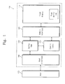
- FIG. 1 is a block diagram illustrating a flash memory system including a multi-level cell (MLC) flash memory according to some embodiments of the present invention.
- MLC multi-level cell
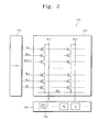
- FIG. 2 is a more detailed block diagram illustrating the MLC flash memory of Figure 1 according to some embodiments of the present invention.
- Figure 3 is a block diagram illustrating a page buffer according to some embodiments of the present invention.
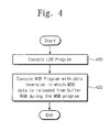
- Figure 4 is a flowchart illustrating operations of a multi-bit program of a multi-bit flash memory according to some embodiments of the present invention.
- FIG. 5 is a flowchart illustrating operations of the LSB program of Figure 4 according to some embodiments of the present invention. (MODIFY THIS FIGURE)
- Figure 6 is a flowchart illustrating operations of the MSB program of Figure 4 according to some embodiments of the present invention.
- Figure 7 is a diagram illustrating a flash memory status distribution according to embodiments of the present invention illustrated in Figures 5 through 7.
- Figure 8 is a diagram illustrating a flash memory status distribution according to embodiments of the present invention illustrated in Figures 5 through 7.
- Figure 9 is a schematic block diagram illustrating page buffer operation during LSB programming of Figure 5 according to some embodiments of the present invention.
- Figure 10 is flowchart illustrating MSB "10" programming of Figure 6 according to some embodiments of the present invention.
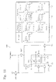
- Figure 11 is a schematic block diagram illustrating MSB "10" page buffer operation of Figure 10 according to some embodiments of the present invention.
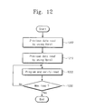
- Figure 12 is a flowchart illustrating MSB "00" programming of Figure 6 according to some embodiments of the present invention.
- Figure 13 is a schematic block diagram illustrating MSB "00" page buffer operation of Figure 12 according to some embodiments of the present invention.
- Figure 14 is a flowchart illustrating MSB "01" programming of Figure 6 according to some embodiments of the present invention.
- Figure 15 is a schematic block diagram illustrating MSB "01" page buffer operation of Figure 14 according to some embodiments of the present invention.
- Figure 16 is a block diagram illustrating flash memory devices according to further embodiments of the present invention.
- Figure 17 is a block diagram illustrating flash memory devices according to still further embodiments of the present invention.
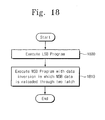
- Figure 18 is a flowchart illustrating operations of the flash memory devices illustrated in Figure 17 according to some embodiments of the present invention.
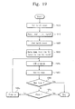
- Figure 19 is a flowchart illustrating operations of LSB programming of Figure 18 according to some embodiments of the present invention.
- Figure 20 is a flowchart illustrating operations of MSB programming of Figure 18 according to some embodiments of the present invention.
- the multi-bit non-volatile memory device includes a memory cell array including a plurality of memory cells and a storage unit electrically coupled to the memory cell array.
- a first bit (FB) of multi-bit data is programmed from the storage unit into one of the plurality of memory cells in the memory cell array and a second bit (SB) of multi-bit data is programmed from the storage unit into one of the plurality of memory cells in the memory cell array using data inversion.
- data inversion for programming the second bit of multi-bit data may allow the multi-bit data to be read with only two read operations, thus decreasing the number of reads required in conventional methods as will be discussed further herein with respect to Figures 1 through 20.
- the system 100 includes a multi-bit flash memory device 105 coupled to an external host device 120.
- the flash memory device 105 includes a memory 110, a memory interface 160, a buffer RAM 180, control logic 170 and a host interface 190.
- the host interface 190 between the multi-bit flash memory device 105 and the external host device 120 may be a NOR interface. It will be understood that the flash memory device 105 can be any flash memory device capable of operating as discussed herein.
- the flash memory device could be a NAND or a NOR flash memory device without departing from the scope of the present invention.
- the flash memory device 105 may be a OneNAND flash memory device.
- the OneNAND flash memory device includes a NAND cell array and a NOR interface between the flash memory device 105 and the host 120.
- the memory 110 may include a page buffer 140 according to some embodiments of the present invention.
- the memory 210 may include a memory cell array 225, a row decoder 230 and a page buffer 240.
- the memory cell array 225 may include one or more memory cells.
- the memory cell array 225 may include a string cell of NAND flash memory.
- the page buffer 240 is electrically coupled to the memory cell array 225 and the buffer RAM 180 (of Figure 1).
- the page buffer 240 may includes one or more single latches 245, which are configured to store a first bit of multi-bit data to be written into or read out from one of the memory cells of the memory cell array 225.
- the first bit of multi-bit data may be the least significant bit (LSB) of multi-bit data.
- the page buffer 240 is also configured store intermediate program data during the programming operation (write operation) as will be further discussed below.
- the page buffer 240 may operate as a driver during a write (program) operation and as a sense amplifier during a read operation.
- the buffer RAM 180 is electrically coupled to the page buffer 240.
- the buffer RAM 180 is configured to store a second bit of the multi-bit data to be written into or read out from one of the memory cells of the memory cell array 225.
- the second bit of multi-bit data is the most significant bit (MSB) of multi-bit data.
- the program data may include MSB intermediate program (write) data as will be discussed further below.
- the buffer RAM 180 may include static RAM (SRAM) or dynamic RAM (DRAM).
- the buffer ram in combination with a single latch page buffer according to some embodiments of the present invention is discussed in detail in commonly assigned United States Patent Application Serial No. 11/801,792, filed on May 11, 2007 entitled MULTI-BIT FLASH MEMORY DEVICES HAVING A SINGLE LATCH STRUCTURE AND RELATED PROGRAMMING METHODS, SYSTEMS AND MEMORY CARDS, the disclosure of which is hereby incorporated herein by reference as if set forth in its entirety.
- the buffer RAM occupies significantly less space than the latches of the page buffer. Therefore, by only including a page buffer 240 having single latches, rather than the conventional double latch, some embodiments of the present invention may provide a more compact and integrated memory device.
- memory devices according to some embodiments of the present invention may be suitable for use in small portable devices, such as mobile terminals and the like.
- control logic block 170 contains the control signals configured to begin and end a programming (write) operation and/or a read operation.
- the buffer RAM 180 may be configured to temporarily store data from the memory cell array 225 through the page buffer 140 in response to a control signal generated by the control logic block 170. Operations of control logic blocks are known to those having skill in the art and will not be discussed in further detail herein in the interest of brevity.
- embodiments of the present invention discussed with respect to Figures 1 and 2 include a buffer RAM 180 and a page buffer 140 as the storage unit, embodiments of the present invention are not limited to this configuration. It will be understood that embodiments of the present invention may include any storage unit configured in accordance with embodiments of the present invention.
- the storage unit is electrically coupled to the memory cell array 225 and configured to store the multi-bit data.
- the storage unit includes a combination of a single latch page buffer and a buffer random access memory (RAM), the first bit of multi-bit data being stored in the single latch page buffer and the second bit of multi-bit data being stored in the buffer RAM as discussed above and in United States Patent Application Serial No. 11/801,792 incorporated by reference above.
- the preprogrammed data may be stored in the single latch page buffer.
- the storage unit may include first and second page buffers 1640 and 1643 as illustrated in Figure 16.
- the first bit of multi-bit data may be stored in one of the page buffers 1640, 1643 and the second bit of multi-bit data may be stored in a second of the page buffers 1640, 1643.
- the first and second page buffers may be upper 1643 and lower 1640 page buffers as illustrated in Figure 16.
- the storage unit may include a double latch page buffer 1750 including first and second latches as illustrated in Figure 17.
- the first bit of multi-bit data may be stored in the first latch 1751 of the double latch page buffer and the second bit of multi-bit data 1753 may be stored in the second latch of the double latch page buffer 1750.
- embodiments of the present invention are discussed above with respect to a two bit multi-bit data having an MSB and an LSB, embodiments of the present invention are not limited to this configuration. Three or more bit multi-bit data may be used without departing from the scope of the present invention.
- a page buffer 300 includes a PMOS transistor M2, first through seventh NMOS transistors M1 and M3 through M8 and three invertors INV 1 through INV3 connected as shown in Figure 3.
- the single latch structure 307 according to embodiments of the present invention includes first and second invertors INV1 and INV2 connected as shown. It will be understood that Figure 3 illustrates a single page buffer cell. Memory devices according to embodiments of the present may include a plurality of these cells as illustrated in the page buffer 245 of Figure 2.
- the page buffer operates responsive to a precharge signal PRE, data received from the memory cell array 225 ( Figure 2) on the bit line (BL), a bit line select signal (BLSLT), data and inverse data signals NDi , Di, DIOp and DIOr and a latch signal (LCH).
- PRE precharge signal
- bit line bit line
- BLSLT bit line select signal
- NDi inverse data signals
- Di Di
- DIOr high a reading operation is being performed.
- LCH latch signal
- FIG. 4 a flowchart illustrating operations of programming methods (writing operations) according to some embodiments of the present invention will be discussed.
- Methods of programming multi-bit non-volatile memory devices are performed in multi-bit non-volatile memory devices including a memory cell array including a plurality of memory cells and a storage unit electrically coupled to the memory cell array as discussed above with respect to Figures 1 through 3 and 16 and 17.
- operations begin at block 400 by programming a first bit (FB) of multi-bit data from the storage unit into one of the plurality of memory cells in the memory cell array.
- the first bit of multi-bit data may be the least significant bit (LSB) according to some embodiments of the present invention.
- operations of block 400 may be executing the LSB program as will be further discussed below.
- Operations continue at block 420 by programming a second bit (SB) of multi-bit data from the storage unit into one of the plurality of memory cells in the memory cell array using data inversion.
- the second bit of multi-bit data may be the most significant bit (MSB) in some embodiments of the present invention.
- operations of block 420 may be executing an MSB program using data inversion. It will be understood that executing of the MSB program (block 420), the data may be reloaded from the buffer RAM 180 ( Figure 1) to the page buffer 140 in accordance with some embodiments of the present invention.
- the step up program (block 565) may be an incremental step pulse program (ISPP), however, embodiments of the present invention are not limited to this configuration.
- the LSB program begins with a cell threshold distribution voltage "11" 701 (the erase state) and ends with a cell threshold distribution of "10" 702.
- this transition may not happen in one programming step, it may take several programming iterations before the final state "10" is achieved, i.e., before the pass (block 555) is generated.
- FIG. 6 a flowchart illustrating operations of most significant bit (MSB) programs according to some embodiments of the present invention will be discussed.
- operations begin at block 607 by executing the MSB "10" program with data inversion.
- the MSB "10" program with data inversion 710 includes bringing data in one of the memory cells whose data is in LSB state "10" (703) before the MSB "10" program operation into MSB state “10” (704) after the MSB "10” program operation.
- data in the storage unit may be inverted and the MSB "10" program may be executed with using the inverted data.
- data inversion data "0" is inhibited and data "1" is programmed.
- the MSB "00" program (block 617) is performed.
- the MSB "00" program operation 720 includes bringing one of the memory cells whose data is in LSB state “10” (706) before the MSB "00” program into state “00” (707) after the MSB "00" program.
- the MSB "01” program block 627) is performed, which provides the second bit of multi-bit data.
- the MSB "01" program operation 730 includes bringing one of the memory cells whose data is in state “11” (708) before the MSB “01” program operation into state “01” (709) after the MSB "01” program operation to provide a programmed second bit of multi-bit data.
- Figures 5 through 7 are based on embodiments with two bit multi-bit data having an LSB and an MSB. Embodiments of the present invention are not limited to this configuration. For example, three or more bit multi-bit data may be used without departing from the scope of the present invention.
- reading the second bit of multi-bit data using two read operations may include applying a first read voltage to one of the memory cells to determine if the state of cell is on or off. Then, a second read voltage is applied to the one of the memory cells to read the second bit of multi-bit data in the one of the memory cells.
- Figure 8 also illustrates the application of a read voltage to one of the memory cells to read the first bit (LSB) of multi-bit data in accordance with embodiments of the present invention.
- the multi-bit data includes data having one of state “0", state “1” , state “2” and state “3.”
- Each of the states has a different threshold voltage.
- an MSB of state “0” is 1 and an LSB of state “0” is 1
- an MSB of state “1” is 0 and an LSB of state “1” is 1
- an MSB of state “2” is 0 and an LSB of state “2” is 0
- an MSB of state “3” is 1 and an LSB of state “3” is 0.
- FIG. 9 a schematic diagram illustrating a page buffer during an LSB program according to some embodiments of the present invention will be discussed. Operations of the page buffer 900 will be discussed in combination with the flowchart of Figure 5. As illustrated in Figure 9, the paths labeled (1) and (1') correspond to a reset of the page buffer 900.
- the partial circuit 910 illustrated in Figure 9 illustrates the values around the first through third invertors INV1 through INV3 during a reset operation. The reset operation corresponds to block 505 of Figure 5.
- the second path labeled (2) of the page buffer 900 corresponds to the data path.
- NDi is always low (“0") and Di is a logic low (“0” or “L”) when the program data is “1” and a logic high (“1") when the program data is a "0".
- NDi is always low ("0")
- Di is a logic low (“0” or “L”) when the program data is "1” and a logic high (“1") when the program data is a "0”.
- data "1" is inhibited and date "0" is programmed.
- the data load operation of the page buffer 900 corresponds to block 515 of the flowchart of Figure 5.
- the third path labeled (3) of the page buffer 900 corresponds to the programming path that programs the memory cell in the memory cell array. Programming corresponds to block 525 of the flowchart of Figure 5.
- the first path labeled (2) of the page buffer 1100 corresponds to the previous data read operation of the memory cell before the data is loaded.
- the partial circuits 1120 in Figure 11 illustrate the alternative values around the first through third invertors INV1 through INV3 during a pre-read operation. Operations of the pre-read operation correspond to block 1019 of the flowchart of Figure 10.
- the second path labeled (3) of the page buffer 1100 corresponds to the data path.
- Di is always low and NDi is a logic high ("1") when the program data is "0" and a logic low ("0" or “L") when the program data is a "1".
- NDi is a logic high ("1") when the program data is "0” and a logic low (“0" or “L") when the program data is a "1".
- the data that is loaded in the page buffer during the MSB"10" operation is inverted.
- data "0" is inhibited and data "1" is programmed.
- the data load operation of the page buffer 1100 of Figure 11 corresponds to block 1029 of the flowchart of Figure 10.
- the fourth path labeled (4) of the page buffer 1100 corresponds to the current path that programs the memory cell in the memory cell array, which corresponds to block 1039 of the flowchart of Figure 10.
- t is determined if the maximum number of iterations have been reached for the MSB "10" program (block 1049). If it is determined that the maximum number of iterations has been reached (block 1049), operations of the MSB "10" program terminate. If, on the other hand, it is determined that the maximum number of iterations has not been reached (block 1049), the word line voltage is stepped up and operations are repeated until either maximum number of iterations is reached (block 1049) or the desired cell threshold voltage distribution is reached.
- the path labeled (1) corresponds to a first previous data read of the page buffer 1300.
- the partial circuit 1310 illustrated in Figure 13 illustrates the values around the first through third invertors INV1 through INV3 during the first previous data read operation. Operations of the first previous data read operation correspond to block 1202 of the flowchart of Figure 12.
- the first path labeled (2) of the page buffer 1300 corresponds to the second pre-read of the memory cell.
- the partial circuits 1320 in Figure 13 illustrate the alternative values around the first through third invertors INV1 through INV3 during the second pre-read operation. Operations of the second previous data read correspond to block 1212 of the flowchart of Figure 12.
- the third path labeled (3) of the page buffer 1300 corresponds to the current path that programs the memory cell in the memory cell array.
- the programming operations of the page buffer 1300 correspond to block 1222 of Figure 12.
- FIG. 15 illustrates the paths labeled (3) and (3') correspond to a reset of the page buffer 1500.
- the partial circuit 1510 illustrated in Figure 15 illustrates the values around the first through third invertors INV1 through INV3 during a reset operation. Operations of the reset correspond to block 1404 of the flowchart of Figure 14.
- the first path labeled (1) illustrates the previous data read according to some embodiments of the present invention.
- the partial circuits 1520 in Figure 15 illustrate the alternative values around the first through third invertors INV1 through INV3 during the previous data read. Operations of the data pre-read correspond to block 1414 of the flowchart of Figure 14.
- the second path labeled (2) of the page buffer 1500 corresponds to a data load of the memory cell.
- the partial circuits 1530 and 1540 in Figure 15 illustrate the alternative values around the first through third invertors INV 1 through INV3 during the data load operation. Operations of the data load operation correspond to block 1424 of the flowchart of Figure 14.
- the fourth path labeled (4) of the page buffer 1500 corresponds to the current path that programs the memory cell in the memory cell array. Programming operations correspond to block 1434 of the flowchart of Figure 14.
- FIG 18 a flowchart illustrating operations according to embodiments of the present invention including a double latch page buffer as illustrated in Figure 17 will be discussed. Operations begin at block 1800 by executing the LSB program. Processing steps in the execution of the LSB program will be discussed further with respect to the flowchart of Figure 19. The MSB program is executed using data inversion where the MSB data is reloaded through the two (double) latch page buffer. Operations of the MSB program will be discussed further with respect to Figure 20.
- FIG. 19 a flowchart illustrating operations of the LSB program in embodiments having a double latch page buffer will be discussed.
- Operations begin at block 1905 by resetting the first latch of the double latch page buffer and then loading the data in the first latch of the double latch page buffer (block 1915).
- the second latch of the double latch page buffer is reset (block 1925) and the second latch of the double latch page buffer is loaded (block 1935).
- the LSB program is executed (block 1945).
- the cell threshold voltage distribution begins at "11" 701 (the erase state).
- a verify read is performed using a read word line voltage (Vvrfl) as shown in Figure 7 (block 1955).
- Vvrfl read word line voltage
- the word line voltage is stepped up (block 1985) and operations of blocks 1945 through 1985 are repeated until either maximum number of iterations is reached (block 1965) or the cell threshold voltage distribution "10" is reached (block 1975).
- the step up program may be an incremental step pulse program (ISPP), however, embodiments of the present invention are not limited to this configuration.
Landscapes
- Engineering & Computer Science (AREA)
- Theoretical Computer Science (AREA)
- Microelectronics & Electronic Packaging (AREA)
- Software Systems (AREA)
- Physics & Mathematics (AREA)
- General Engineering & Computer Science (AREA)
- General Physics & Mathematics (AREA)
- Computer Hardware Design (AREA)
- Read Only Memory (AREA)
- Non-Volatile Memory (AREA)
Priority Applications (1)
| Application Number | Priority Date | Filing Date | Title |
|---|---|---|---|
| US11/843,219 US7684238B2 (en) | 2006-08-24 | 2007-08-22 | Methods of programming multi-bit flash memory devices and related devices |
Applications Claiming Priority (1)
| Application Number | Priority Date | Filing Date | Title |
|---|---|---|---|
| KR1020060080698A KR100919156B1 (ko) | 2006-08-24 | 2006-08-24 | 멀티-비트 플래시 메모리 장치 및 그것의 프로그램 방법 |
Publications (2)
| Publication Number | Publication Date |
|---|---|
| EP1892721A2 true EP1892721A2 (de) | 2008-02-27 |
| EP1892721A3 EP1892721A3 (de) | 2008-07-30 |
Family
ID=38640086
Family Applications (1)
| Application Number | Title | Priority Date | Filing Date |
|---|---|---|---|
| EP07016055A Withdrawn EP1892721A3 (de) | 2006-08-24 | 2007-08-16 | Verfahren zur Programmierung einer nichtflüchtigen Multi-Bit-Speichervorrichtung und nichtflüchtige Multi-Bit-Speichervorrichtung |
Country Status (5)
| Country | Link |
|---|---|
| US (1) | US7684238B2 (de) |
| EP (1) | EP1892721A3 (de) |
| JP (1) | JP5825749B2 (de) |
| KR (1) | KR100919156B1 (de) |
| CN (1) | CN101145396B (de) |
Cited By (1)
| Publication number | Priority date | Publication date | Assignee | Title |
|---|---|---|---|---|
| TWI496149B (zh) * | 2013-01-31 | 2015-08-11 | Ememory Technology Inc | 快閃記憶體及其相關程劃方法 |
Families Citing this family (75)
| Publication number | Priority date | Publication date | Assignee | Title |
|---|---|---|---|---|
| WO2009095902A2 (en) | 2008-01-31 | 2009-08-06 | Densbits Technologies Ltd. | Systems and methods for handling immediate data errors in flash memory |
| KR101292574B1 (ko) * | 2007-10-08 | 2013-08-16 | 삼성전자주식회사 | 멀티 비트 프로그래밍 장치 및 방법 |
| US8694715B2 (en) | 2007-10-22 | 2014-04-08 | Densbits Technologies Ltd. | Methods for adaptively programming flash memory devices and flash memory systems incorporating same |
| US7679972B2 (en) * | 2007-11-19 | 2010-03-16 | Spansion Llc | High reliable and low power static random access memory |
| WO2009072100A2 (en) | 2007-12-05 | 2009-06-11 | Densbits Technologies Ltd. | Systems and methods for temporarily retiring memory portions |
| WO2009074978A2 (en) | 2007-12-12 | 2009-06-18 | Densbits Technologies Ltd. | Systems and methods for error correction and decoding on multi-level physical media |
| WO2009118720A2 (en) | 2008-03-25 | 2009-10-01 | Densbits Technologies Ltd. | Apparatus and methods for hardware-efficient unbiased rounding |
| US7729166B2 (en) * | 2008-07-02 | 2010-06-01 | Mosaid Technologies Incorporated | Multiple-bit per cell (MBC) non-volatile memory apparatus and system having polarity control and method of programming same |
| JP2010140521A (ja) * | 2008-12-09 | 2010-06-24 | Powerchip Semiconductor Corp | 不揮発性半導体記憶装置とその読み出し方法 |
| KR20100107294A (ko) | 2009-03-25 | 2010-10-05 | 삼성전자주식회사 | 불휘발성 메모리 장치를 포함하는 메모리 시스템 및 불휘발성 메모리 장치의 프로그램 방법 |
| US8819385B2 (en) | 2009-04-06 | 2014-08-26 | Densbits Technologies Ltd. | Device and method for managing a flash memory |
| US8458574B2 (en) * | 2009-04-06 | 2013-06-04 | Densbits Technologies Ltd. | Compact chien-search based decoding apparatus and method |
| US20100332922A1 (en) * | 2009-06-30 | 2010-12-30 | Mediatek Inc. | Method for managing device and solid state disk drive utilizing the same |
| US8130543B2 (en) * | 2009-08-13 | 2012-03-06 | Macronix International Co., Ltd. | Method and apparatus for increasing memory programming efficiency through dynamic switching of sense amplifiers |
| US8995197B1 (en) | 2009-08-26 | 2015-03-31 | Densbits Technologies Ltd. | System and methods for dynamic erase and program control for flash memory device memories |
| US9330767B1 (en) | 2009-08-26 | 2016-05-03 | Avago Technologies General Ip (Singapore) Pte. Ltd. | Flash memory module and method for programming a page of flash memory cells |
| US8730729B2 (en) | 2009-10-15 | 2014-05-20 | Densbits Technologies Ltd. | Systems and methods for averaging error rates in non-volatile devices and storage systems |
| US8724387B2 (en) | 2009-10-22 | 2014-05-13 | Densbits Technologies Ltd. | Method, system, and computer readable medium for reading and programming flash memory cells using multiple bias voltages |
| US9037777B2 (en) * | 2009-12-22 | 2015-05-19 | Densbits Technologies Ltd. | Device, system, and method for reducing program/read disturb in flash arrays |
| KR101829208B1 (ko) | 2009-12-31 | 2018-02-20 | 에스케이하이닉스 주식회사 | 반도체 메모리 장치의 동작 방법 |
| KR101626080B1 (ko) * | 2010-02-17 | 2016-06-01 | 삼성전자주식회사 | 페이지 버퍼 관리 방법과 상기 방법을 수행할 수 있는 장치들 |
| US8516274B2 (en) * | 2010-04-06 | 2013-08-20 | Densbits Technologies Ltd. | Method, system and medium for analog encryption in a flash memory |
| US8745317B2 (en) | 2010-04-07 | 2014-06-03 | Densbits Technologies Ltd. | System and method for storing information in a multi-level cell memory |
| US8468431B2 (en) | 2010-07-01 | 2013-06-18 | Densbits Technologies Ltd. | System and method for multi-dimensional encoding and decoding |
| US8508992B2 (en) * | 2010-07-09 | 2013-08-13 | SK Hynix Inc. | Semiconductor memory device and method of operating the same |
| WO2012009812A1 (en) * | 2010-07-21 | 2012-01-26 | Mosaid Technologies Incorporated | Multipage program scheme for flash memory |
| US8964464B2 (en) | 2010-08-24 | 2015-02-24 | Densbits Technologies Ltd. | System and method for accelerated sampling |
| US9063878B2 (en) | 2010-11-03 | 2015-06-23 | Densbits Technologies Ltd. | Method, system and computer readable medium for copy back |
| US8850100B2 (en) | 2010-12-07 | 2014-09-30 | Densbits Technologies Ltd. | Interleaving codeword portions between multiple planes and/or dies of a flash memory device |
| US8990665B1 (en) | 2011-04-06 | 2015-03-24 | Densbits Technologies Ltd. | System, method and computer program product for joint search of a read threshold and soft decoding |
| US9110785B1 (en) | 2011-05-12 | 2015-08-18 | Densbits Technologies Ltd. | Ordered merge of data sectors that belong to memory space portions |
| US9501392B1 (en) | 2011-05-12 | 2016-11-22 | Avago Technologies General Ip (Singapore) Pte. Ltd. | Management of a non-volatile memory module |
| US9195592B1 (en) | 2011-05-12 | 2015-11-24 | Densbits Technologies Ltd. | Advanced management of a non-volatile memory |
| US9372792B1 (en) | 2011-05-12 | 2016-06-21 | Avago Technologies General Ip (Singapore) Pte. Ltd. | Advanced management of a non-volatile memory |
| US9396106B2 (en) | 2011-05-12 | 2016-07-19 | Avago Technologies General Ip (Singapore) Pte. Ltd. | Advanced management of a non-volatile memory |
| US8996790B1 (en) | 2011-05-12 | 2015-03-31 | Densbits Technologies Ltd. | System and method for flash memory management |
| JP2013041634A (ja) * | 2011-08-11 | 2013-02-28 | Fujitsu Ltd | 不揮発性半導体記憶装置 |
| US8947941B2 (en) | 2012-02-09 | 2015-02-03 | Densbits Technologies Ltd. | State responsive operations relating to flash memory cells |
| US8996788B2 (en) | 2012-02-09 | 2015-03-31 | Densbits Technologies Ltd. | Configurable flash interface |
| US8996793B1 (en) | 2012-04-24 | 2015-03-31 | Densbits Technologies Ltd. | System, method and computer readable medium for generating soft information |
| US8838937B1 (en) | 2012-05-23 | 2014-09-16 | Densbits Technologies Ltd. | Methods, systems and computer readable medium for writing and reading data |
| US8879325B1 (en) | 2012-05-30 | 2014-11-04 | Densbits Technologies Ltd. | System, method and computer program product for processing read threshold information and for reading a flash memory module |
| US9921954B1 (en) | 2012-08-27 | 2018-03-20 | Avago Technologies General Ip (Singapore) Pte. Ltd. | Method and system for split flash memory management between host and storage controller |
| KR102040904B1 (ko) | 2012-11-05 | 2019-11-05 | 에스케이하이닉스 주식회사 | 반도체 메모리 장치 및 이의 동작 방법 |
| US9368225B1 (en) | 2012-11-21 | 2016-06-14 | Avago Technologies General Ip (Singapore) Pte. Ltd. | Determining read thresholds based upon read error direction statistics |
| US9069659B1 (en) | 2013-01-03 | 2015-06-30 | Densbits Technologies Ltd. | Read threshold determination using reference read threshold |
| US9136876B1 (en) | 2013-06-13 | 2015-09-15 | Densbits Technologies Ltd. | Size limited multi-dimensional decoding |
| US9413491B1 (en) | 2013-10-08 | 2016-08-09 | Avago Technologies General Ip (Singapore) Pte. Ltd. | System and method for multiple dimension decoding and encoding a message |
| US9348694B1 (en) | 2013-10-09 | 2016-05-24 | Avago Technologies General Ip (Singapore) Pte. Ltd. | Detecting and managing bad columns |
| US9786388B1 (en) | 2013-10-09 | 2017-10-10 | Avago Technologies General Ip (Singapore) Pte. Ltd. | Detecting and managing bad columns |
| US9397706B1 (en) | 2013-10-09 | 2016-07-19 | Avago Technologies General Ip (Singapore) Pte. Ltd. | System and method for irregular multiple dimension decoding and encoding |
| US9536612B1 (en) | 2014-01-23 | 2017-01-03 | Avago Technologies General Ip (Singapore) Pte. Ltd | Digital signaling processing for three dimensional flash memory arrays |
| US10120792B1 (en) | 2014-01-29 | 2018-11-06 | Avago Technologies General Ip (Singapore) Pte. Ltd. | Programming an embedded flash storage device |
| US9542262B1 (en) | 2014-05-29 | 2017-01-10 | Avago Technologies General Ip (Singapore) Pte. Ltd. | Error correction |
| US9892033B1 (en) | 2014-06-24 | 2018-02-13 | Avago Technologies General Ip (Singapore) Pte. Ltd. | Management of memory units |
| US9584159B1 (en) | 2014-07-03 | 2017-02-28 | Avago Technologies General Ip (Singapore) Pte. Ltd. | Interleaved encoding |
| US9972393B1 (en) | 2014-07-03 | 2018-05-15 | Avago Technologies General Ip (Singapore) Pte. Ltd. | Accelerating programming of a flash memory module |
| US9449702B1 (en) | 2014-07-08 | 2016-09-20 | Avago Technologies General Ip (Singapore) Pte. Ltd. | Power management |
| KR20160044923A (ko) * | 2014-10-16 | 2016-04-26 | 에스케이하이닉스 주식회사 | 복수의 메모리 셀들을 포함하는 반도체 메모리 장치 및 그것의 동작 방법 |
| US9524211B1 (en) | 2014-11-18 | 2016-12-20 | Avago Technologies General Ip (Singapore) Pte. Ltd. | Codeword management |
| KR102239868B1 (ko) * | 2014-11-28 | 2021-04-13 | 에스케이하이닉스 주식회사 | 메모리 시스템 및 그것의 동작 방법 |
| KR102271462B1 (ko) | 2015-01-13 | 2021-07-05 | 삼성전자주식회사 | 불휘발성 메모리 장치, 그것의 동작 방법, 및 그것의 프로그램 방법 |
| US10305515B1 (en) | 2015-02-02 | 2019-05-28 | Avago Technologies International Sales Pte. Limited | System and method for encoding using multiple linear feedback shift registers |
| JP2016173868A (ja) * | 2015-03-17 | 2016-09-29 | 株式会社東芝 | 不揮発性半導体記憶装置 |
| TWI550612B (zh) * | 2015-03-23 | 2016-09-21 | 群聯電子股份有限公司 | 資料程式化方法、記憶體儲存裝置及記憶體控制電路單元 |
| US10628255B1 (en) | 2015-06-11 | 2020-04-21 | Avago Technologies International Sales Pte. Limited | Multi-dimensional decoding |
| US9851921B1 (en) | 2015-07-05 | 2017-12-26 | Avago Technologies General Ip (Singapore) Pte. Ltd. | Flash memory chip processing |
| US10466908B2 (en) * | 2015-08-25 | 2019-11-05 | Toshiba Memory Corporation | Memory system that buffers data before writing to nonvolatile memory |
| KR102329800B1 (ko) * | 2015-10-22 | 2021-11-22 | 삼성전자주식회사 | 메모리 장치 및 메모리 장치의 에지 워드라인 관리 방법 |
| US9954558B1 (en) | 2016-03-03 | 2018-04-24 | Avago Technologies General Ip (Singapore) Pte. Ltd. | Fast decoding of data stored in a flash memory |
| JP2018005959A (ja) * | 2016-06-30 | 2018-01-11 | 東芝メモリ株式会社 | メモリシステムおよび書き込み方法 |
| US20180039427A1 (en) * | 2016-08-08 | 2018-02-08 | Nuvoton Technology Corporation | Reducing programming time of memory devices using data encoding |
| KR102736266B1 (ko) | 2018-10-29 | 2024-12-02 | 에스케이하이닉스 주식회사 | 저장 장치 및 그 동작 방법 |
| JP2020102286A (ja) * | 2018-12-21 | 2020-07-02 | キオクシア株式会社 | 半導体記憶装置 |
| CN109859683B (zh) * | 2019-04-12 | 2023-08-04 | 深圳市德普微电子有限公司 | 一种led显示屏单双锁存自动切换芯片 |
Citations (4)
| Publication number | Priority date | Publication date | Assignee | Title |
|---|---|---|---|---|
| US6288935B1 (en) | 1999-09-20 | 2001-09-11 | Kabushiki Kaisha Toshiba | Nonvolatile semiconductor memory device for storing multivalued data |
| EP1280161A1 (de) | 2001-07-23 | 2003-01-29 | Samsung Electronics Co., Ltd. | Speicheranordnung mit einem zwei Register enthaltenden Seitenpufferspeicher sowie entsprechendes Benutzungsverfahren |
| US6522580B2 (en) | 2001-06-27 | 2003-02-18 | Sandisk Corporation | Operating techniques for reducing effects of coupling between storage elements of a non-volatile memory operated in multiple data states |
| US7023737B1 (en) | 2005-08-01 | 2006-04-04 | Sandisk Corporation | System for programming non-volatile memory with self-adjusting maximum program loop |
Family Cites Families (53)
| Publication number | Priority date | Publication date | Assignee | Title |
|---|---|---|---|---|
| KR960000616B1 (ko) | 1993-01-13 | 1996-01-10 | 삼성전자주식회사 | 불휘발성 반도체 메모리 장치 |
| JP3153730B2 (ja) * | 1995-05-16 | 2001-04-09 | 株式会社東芝 | 不揮発性半導体記憶装置 |
| KR0172408B1 (ko) | 1995-12-11 | 1999-03-30 | 김광호 | 다수상태 불휘발성 반도체 메모리 및 그의 구동방법 |
| US5724284A (en) | 1996-06-24 | 1998-03-03 | Advanced Micro Devices, Inc. | Multiple bits-per-cell flash shift register page buffer |
| US6166950A (en) | 1996-07-10 | 2000-12-26 | Hitachi, Ltd. | Nonvolatile semiconductor storage device |
| US6335878B1 (en) | 1998-07-28 | 2002-01-01 | Hitachi, Ltd. | Non-volatile multi-level semiconductor flash memory device and method of driving same |
| JPH1092186A (ja) * | 1996-09-12 | 1998-04-10 | Hitachi Ltd | 半導体記憶装置 |
| KR100205240B1 (ko) | 1996-09-13 | 1999-07-01 | 윤종용 | 단일 비트 및 다중 비트 셀들이 장착된 불휘발성 반도체 메모리 장치 |
| KR100206709B1 (ko) | 1996-09-21 | 1999-07-01 | 윤종용 | 멀티비트 불휘발성 반도체 메모리의 셀 어레이의 구조 및 그의 구동방법 |
| US5862074A (en) | 1996-10-04 | 1999-01-19 | Samsung Electronics Co., Ltd. | Integrated circuit memory devices having reconfigurable nonvolatile multi-bit memory cells therein and methods of operating same |
| KR100259972B1 (ko) | 1997-01-21 | 2000-06-15 | 윤종용 | 메모리 셀당 2개 이상의 저장 상태들을 갖는 불휘발성 반도체 메모리 장치 |
| JP3156636B2 (ja) * | 1997-05-30 | 2001-04-16 | 日本電気株式会社 | 不揮発性半導体記憶装置 |
| JPH11144479A (ja) | 1997-11-10 | 1999-05-28 | New Koa Technology Kk | 不揮発性半導体多値メモリ装置 |
| US5867429A (en) | 1997-11-19 | 1999-02-02 | Sandisk Corporation | High density non-volatile flash memory without adverse effects of electric field coupling between adjacent floating gates |
| KR100266744B1 (ko) | 1997-12-29 | 2000-09-15 | 윤종용 | 고집적 가능한 멀티-비트 데이터 래치 회로를 갖는 반도체 메모리 장치 |
| KR100266745B1 (ko) | 1997-12-29 | 2000-09-15 | 윤종용 | 멀티-비트 데이터를 저장하기 위한 반도체 메모리 장치 |
| KR100295135B1 (ko) | 1997-12-31 | 2001-07-12 | 윤종용 | 멀티-비트 셀 구조를 갖는 비휘발성 메모리 장치 |
| US5930172A (en) | 1998-06-23 | 1999-07-27 | Advanced Micro Devices, Inc. | Page buffer for a multi-level flash memory with a limited number of latches per memory cell |
| JP2000215679A (ja) * | 1999-01-18 | 2000-08-04 | Taito Corp | 半導体記憶装置 |
| KR100347866B1 (ko) * | 1999-03-08 | 2002-08-09 | 삼성전자 주식회사 | 낸드 플래시 메모리 장치 |
| KR20010068554A (ko) | 2000-01-06 | 2001-07-23 | 김헌배 | 차량 엔진의 고장상태를 진단하는 장치 |
| US6266273B1 (en) | 2000-08-21 | 2001-07-24 | Sandisk Corporation | Method and structure for reliable data copy operation for non-volatile memories |
| KR100386296B1 (ko) * | 2000-12-30 | 2003-06-02 | 주식회사 하이닉스반도체 | 멀티레벨을 가지는 플래쉬 메모리를 프로그램/리드하기위한 회로 및 그 방법 |
| KR100390959B1 (ko) * | 2001-06-29 | 2003-07-12 | 주식회사 하이닉스반도체 | 센싱회로를 이용한 멀티레벨 플래시 메모리 프로그램/리드방법 |
| JP2003030993A (ja) | 2001-07-17 | 2003-01-31 | Toshiba Corp | 半導体記憶装置 |
| US7042770B2 (en) * | 2001-07-23 | 2006-05-09 | Samsung Electronics Co., Ltd. | Memory devices with page buffer having dual registers and method of using the same |
| JP4122750B2 (ja) * | 2001-10-24 | 2008-07-23 | 沖電気工業株式会社 | 半導体記憶装置および半導体記憶装置のデータ書き込み方法 |
| KR100855504B1 (ko) | 2001-12-08 | 2008-09-01 | 엘지디스플레이 주식회사 | 액정표시소자의 제조방법 |
| US6687158B2 (en) * | 2001-12-21 | 2004-02-03 | Fujitsu Limited | Gapless programming for a NAND type flash memory |
| KR100437461B1 (ko) | 2002-01-12 | 2004-06-23 | 삼성전자주식회사 | 낸드 플래시 메모리 장치 및 그것의 소거, 프로그램,그리고 카피백 프로그램 방법 |
| KR100466980B1 (ko) | 2002-01-15 | 2005-01-24 | 삼성전자주식회사 | 낸드 플래시 메모리 장치 |
| JP4082913B2 (ja) | 2002-02-07 | 2008-04-30 | 株式会社ルネサステクノロジ | メモリシステム |
| US6549457B1 (en) * | 2002-02-15 | 2003-04-15 | Intel Corporation | Using multiple status bits per cell for handling power failures during write operations |
| JP3935139B2 (ja) * | 2002-11-29 | 2007-06-20 | 株式会社東芝 | 半導体記憶装置 |
| JP4294977B2 (ja) * | 2003-02-28 | 2009-07-15 | 株式会社ルネサステクノロジ | 不揮発性記憶装置 |
| JP4563715B2 (ja) | 2003-04-29 | 2010-10-13 | 三星電子株式会社 | パーシャルコピーバック動作モードを有するフラッシュメモリ装置 |
| KR100512181B1 (ko) | 2003-07-11 | 2005-09-05 | 삼성전자주식회사 | 멀티 레벨 셀을 갖는 플래시 메모리 장치와 그것의 독출방법 및 프로그램 방법 |
| JP4041057B2 (ja) * | 2003-11-13 | 2008-01-30 | 株式会社東芝 | 不揮発性半導体記憶装置 |
| KR100541819B1 (ko) | 2003-12-30 | 2006-01-10 | 삼성전자주식회사 | 스타트 프로그램 전압을 차등적으로 사용하는 불휘발성반도체 메모리 장치 및 그에 따른 프로그램 방법 |
| KR100528482B1 (ko) | 2003-12-31 | 2005-11-15 | 삼성전자주식회사 | 데이타를 섹터 단위로 랜덤하게 입출력할 수 있는 플래시메모리 시스템 |
| KR100525004B1 (ko) * | 2004-02-26 | 2005-10-31 | 삼성전자주식회사 | 멀티레벨 셀(Multi-level cell)플래쉬메모리장치 및 이의 프로그램 방법 |
| JP2005353171A (ja) | 2004-06-10 | 2005-12-22 | Toshiba Corp | 半導体記憶装置及びそのブランクページ検索方法 |
| KR100568116B1 (ko) | 2004-09-13 | 2006-04-05 | 삼성전자주식회사 | 전압 조절 수단을 구비한 플래시 메모리 장치 |
| JP4410188B2 (ja) * | 2004-11-12 | 2010-02-03 | 株式会社東芝 | 半導体記憶装置のデータ書き込み方法 |
| US7298648B2 (en) * | 2004-11-19 | 2007-11-20 | Samsung Electronics Co., Ltd. | Page buffer and multi-state nonvolatile memory device including the same |
| JP4768256B2 (ja) * | 2004-12-16 | 2011-09-07 | 株式会社東芝 | 半導体記憶装置 |
| KR100597788B1 (ko) * | 2004-12-17 | 2006-07-06 | 삼성전자주식회사 | 프로그램 동작 속도를 개선하는 불휘발성 반도체 메모리장치의 페이지 버퍼와 이에 대한 구동방법 |
| US7187583B2 (en) | 2005-01-25 | 2007-03-06 | Phison Electronics Corp. | Method for reducing data error when flash memory storage device using copy back command |
| KR100672148B1 (ko) * | 2005-02-17 | 2007-01-19 | 주식회사 하이닉스반도체 | 불휘발성 메모리 장치 및 그것의 페이지 버퍼 동작 방법 |
| KR100597063B1 (ko) | 2005-04-08 | 2006-07-06 | 후지쯔 가부시끼가이샤 | 플래시 메모리 및 메모리 제어 방법 |
| JP4874566B2 (ja) * | 2005-04-11 | 2012-02-15 | 株式会社東芝 | 半導体記憶装置 |
| KR100721012B1 (ko) * | 2005-07-12 | 2007-05-22 | 삼성전자주식회사 | 낸드 플래시 메모리 장치 및 그것의 프로그램 방법 |
| KR101247247B1 (ko) | 2005-11-30 | 2013-03-25 | 삼성전자주식회사 | 클락 신호의 출력을 제어할 수 있는 컨트롤러 및 상기 컨트롤러를 구비하는 시스템 |
-
2006
- 2006-08-24 KR KR1020060080698A patent/KR100919156B1/ko not_active Expired - Fee Related
-
2007
- 2007-08-16 EP EP07016055A patent/EP1892721A3/de not_active Withdrawn
- 2007-08-22 US US11/843,219 patent/US7684238B2/en active Active
- 2007-08-24 CN CN2007101701193A patent/CN101145396B/zh active Active
- 2007-08-24 JP JP2007218927A patent/JP5825749B2/ja active Active
Patent Citations (4)
| Publication number | Priority date | Publication date | Assignee | Title |
|---|---|---|---|---|
| US6288935B1 (en) | 1999-09-20 | 2001-09-11 | Kabushiki Kaisha Toshiba | Nonvolatile semiconductor memory device for storing multivalued data |
| US6522580B2 (en) | 2001-06-27 | 2003-02-18 | Sandisk Corporation | Operating techniques for reducing effects of coupling between storage elements of a non-volatile memory operated in multiple data states |
| EP1280161A1 (de) | 2001-07-23 | 2003-01-29 | Samsung Electronics Co., Ltd. | Speicheranordnung mit einem zwei Register enthaltenden Seitenpufferspeicher sowie entsprechendes Benutzungsverfahren |
| US7023737B1 (en) | 2005-08-01 | 2006-04-04 | Sandisk Corporation | System for programming non-volatile memory with self-adjusting maximum program loop |
Cited By (1)
| Publication number | Priority date | Publication date | Assignee | Title |
|---|---|---|---|---|
| TWI496149B (zh) * | 2013-01-31 | 2015-08-11 | Ememory Technology Inc | 快閃記憶體及其相關程劃方法 |
Also Published As
| Publication number | Publication date |
|---|---|
| US7684238B2 (en) | 2010-03-23 |
| JP2008052899A (ja) | 2008-03-06 |
| US20080049497A1 (en) | 2008-02-28 |
| CN101145396A (zh) | 2008-03-19 |
| KR20080018495A (ko) | 2008-02-28 |
| JP5825749B2 (ja) | 2015-12-02 |
| CN101145396B (zh) | 2013-09-18 |
| KR100919156B1 (ko) | 2009-09-28 |
| EP1892721A3 (de) | 2008-07-30 |
Similar Documents
| Publication | Publication Date | Title |
|---|---|---|
| US7684238B2 (en) | Methods of programming multi-bit flash memory devices and related devices | |
| US7643339B2 (en) | Multi-bit flash memory devices having a single latch structure and related programming methods, systems and memory cards | |
| KR100732628B1 (ko) | 멀티-비트 데이터 및 싱글-비트 데이터를 저장하는 플래시메모리 장치 | |
| US7463526B2 (en) | Programming method for flash memory capable of compensating reduction of read margin between states due to high temperature stress | |
| US8897066B2 (en) | Method of programming nonvolatile memory device | |
| US7468907B2 (en) | Programming method for flash memory capable of compensating reduction of read margin between states due to hot temperature stress | |
| US7738294B2 (en) | Programming multilevel cell memory arrays | |
| JP3420121B2 (ja) | 不揮発性半導体記憶装置 | |
| JP5241080B2 (ja) | Nandフラッシュメモリ装置及びそのプログラム方法 | |
| US20080144370A1 (en) | Method of programming multi-level cells and non-volatile memory device including the same | |
| TW201447889A (zh) | 提供寫入中止保護之寫入序列 | |
| JP2008204598A (ja) | メモリ素子およびプログラム検証方法 | |
| JP4977843B2 (ja) | 面積が減少したページバッファ回路とその読み出し及びプログラム動作方法 | |
| US8189394B2 (en) | Page buffer circuit of nonvolatile memory device and method of operating the same | |
| JP2010287306A (ja) | データ値分布に基づいてプログラム状態決定を利用するメモリ装置、及びその駆動方法 | |
| JP4560073B2 (ja) | 不揮発性半導体記憶装置 | |
| CN110782931B (zh) | 用于非易失静态随机存取存储器架构的扩展写入模式 | |
| JP4931404B2 (ja) | 不揮発性メモリ装置 | |
| JP4750034B2 (ja) | 半導体装置および書き込み方法 | |
| US20080310226A1 (en) | Multi-Bit Flash Memory Devices Having a Single Latch Structure and Related Programming Methods, Systems and Memory Cards | |
| US20070171726A1 (en) | Program method of flash memory capable of compensating reduction of read margin between states due to hot temperature stress | |
| JPH09326199A (ja) | 不揮発性半導体記憶装置 | |
| US7362612B2 (en) | Program method for flash memory capable of compensating for the reduction of read margin between states | |
| JP2007087563A (ja) | フラッシュメモリ装置のページバッファおよびそれを用いたプログラム方法 | |
| US20080151641A1 (en) | Non-volatile memory device reducing data programming and verification time, and method of driving the same |
Legal Events
| Date | Code | Title | Description |
|---|---|---|---|
| PUAI | Public reference made under article 153(3) epc to a published international application that has entered the european phase |
Free format text: ORIGINAL CODE: 0009012 |
|
| AK | Designated contracting states |
Kind code of ref document: A2 Designated state(s): AT BE BG CH CY CZ DE DK EE ES FI FR GB GR HU IE IS IT LI LT LU LV MC MT NL PL PT RO SE SI SK TR |
|
| AX | Request for extension of the european patent |
Extension state: AL BA HR MK YU |
|
| PUAL | Search report despatched |
Free format text: ORIGINAL CODE: 0009013 |
|
| AK | Designated contracting states |
Kind code of ref document: A3 Designated state(s): AT BE BG CH CY CZ DE DK EE ES FI FR GB GR HU IE IS IT LI LT LU LV MC MT NL PL PT RO SE SI SK TR |
|
| AX | Request for extension of the european patent |
Extension state: AL BA HR MK RS |
|
| 17P | Request for examination filed |
Effective date: 20090126 |
|
| 17Q | First examination report despatched |
Effective date: 20090303 |
|
| AKX | Designation fees paid |
Designated state(s): DE |
|
| STAA | Information on the status of an ep patent application or granted ep patent |
Free format text: STATUS: THE APPLICATION IS DEEMED TO BE WITHDRAWN |
|
| 18D | Application deemed to be withdrawn |
Effective date: 20110301 |