EP1895413A2 - Zugangsüberwachungsverfahren und Vorrichtung für gemeinsamen Speicher - Google Patents
Zugangsüberwachungsverfahren und Vorrichtung für gemeinsamen Speicher Download PDFInfo
- Publication number
- EP1895413A2 EP1895413A2 EP07015874A EP07015874A EP1895413A2 EP 1895413 A2 EP1895413 A2 EP 1895413A2 EP 07015874 A EP07015874 A EP 07015874A EP 07015874 A EP07015874 A EP 07015874A EP 1895413 A2 EP1895413 A2 EP 1895413A2
- Authority
- EP
- European Patent Office
- Prior art keywords
- access right
- request
- identifier
- shared memory
- acquisition
- Prior art date
- Legal status (The legal status is an assumption and is not a legal conclusion. Google has not performed a legal analysis and makes no representation as to the accuracy of the status listed.)
- Withdrawn
Links
Images


Classifications
-
- G—PHYSICS
- G06—COMPUTING OR CALCULATING; COUNTING
- G06F—ELECTRIC DIGITAL DATA PROCESSING
- G06F12/00—Accessing, addressing or allocating within memory systems or architectures
- G06F12/02—Addressing or allocation; Relocation
- G06F12/08—Addressing or allocation; Relocation in hierarchically structured memory systems, e.g. virtual memory systems
- G06F12/0802—Addressing of a memory level in which the access to the desired data or data block requires associative addressing means, e.g. caches
- G06F12/0806—Multiuser, multiprocessor or multiprocessing cache systems
- G06F12/0815—Cache consistency protocols
- G06F12/0831—Cache consistency protocols using a bus scheme, e.g. with bus monitoring or watching means
-
- G—PHYSICS
- G06—COMPUTING OR CALCULATING; COUNTING
- G06F—ELECTRIC DIGITAL DATA PROCESSING
- G06F9/00—Arrangements for program control, e.g. control units
- G06F9/06—Arrangements for program control, e.g. control units using stored programs, i.e. using an internal store of processing equipment to receive or retain programs
- G06F9/46—Multiprogramming arrangements
- G06F9/52—Program synchronisation; Mutual exclusion, e.g. by means of semaphores
- G06F9/526—Mutual exclusion algorithms
-
- G—PHYSICS
- G06—COMPUTING OR CALCULATING; COUNTING
- G06F—ELECTRIC DIGITAL DATA PROCESSING
- G06F12/00—Accessing, addressing or allocating within memory systems or architectures
- G06F12/02—Addressing or allocation; Relocation
- G06F12/08—Addressing or allocation; Relocation in hierarchically structured memory systems, e.g. virtual memory systems
- G06F12/0802—Addressing of a memory level in which the access to the desired data or data block requires associative addressing means, e.g. caches
- G06F12/0806—Multiuser, multiprocessor or multiprocessing cache systems
- G06F12/0813—Multiuser, multiprocessor or multiprocessing cache systems with a network or matrix configuration
Definitions
- the present invention relates to an access monitoring method and device for shared memory, and in particular to an access monitoring method and device for shared memory in a multi-processor system where a plurality of processors access a shared memory.
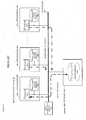
- a multi-processor system 10 shown in Fig. 11 is composed of a shared memory board 100 on which a shared memory SM is mounted, processor boards 200_1-200_n (hereinafter, occasionally represented by a reference numeral 200) on which "n" units of processors 210_1-210_n (hereinafter, occasionally represented by a reference numeral 210) connected to the shared memory board 100 through a common bus CB and "n" units of cache memories CM1-CMn (hereinafter, occasionally represented by a reference character CM) are respectively mounted, and a bus arbitration device 300 connected to the common bus CB to arbitrate accesses to the shared memory SM from the processors 210_1-210_n, which is generally called a common bus type multi-processor system.
- processor boards 200_1-200_n hereinafter, occasionally represented by a reference numeral 200
- CM1-CMn hereinafter, occasionally represented by a reference character CM
- the other processors 210_2-210_n respectively monitor (snoop) through the common bus CB access information (namely, information indicating whether or not the arbitrary processor is accessing the shared memory SM) as well as the date read or written, so that the access information and the data read or written are reflected in the cache memories CM2-CMn as shown by the dashed-dotted lines in Fig.11.
- each processor 210 can acquire the latest data of the shared memory SM by having only to access the cache memory CM within its own processor board 200, thereby reducing a processing time required for accessing the shared memory SM.
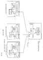
- a multi-processor system 10 shown in Fig. 10 the processor boards 200_1-200_n are respectively connected to the shared memory board 100 one-on-one with "n" sets of serial buses SB, different from the arrangement described in the above-mentioned prior art example [1].
- This system is generally called a star type multi-processor system.
- the processor boards 200_1-200_n and the shared memory board 100 respectively have bus interfaces 220_1-220_n and 110 controlling the access to the shared memory SM.
- the bus interfaces 220_1-220_n and 110 are mutually connected, so that the processors 210_1-210_n and the cache memories CM1-CMn are connected to the shared memory SM through processor buses PB1-PBn; as well as the bus interfaces 220_1-220_n and 110.
- each of the processors 210_1-210n can respectively access the shared memory SM in parallel, so that the data write in the shared memory SM can be performed at an arbitrary timing, and only necessary data can be read from the shared memory SM to be stored in the cache memory CM (see e.g. patent documents 1-3).
- Patent document 1 Japanese Patent Application Laid-open No.58-016362
- Patent document 2 Japanese Patent Application Laid-open No.2000-267815
- Patent document 3 Japanese Patent Application Laid-open No.2000-267816
- a delay may occur by having other processors which request an access without recognizing the access to the shared memory by a certain processor wait for the access to the shared memory. Also, a transaction load due to concurrent requests of access to the shared memory from the processors may degrade the throughput of the whole system.
- an answer packet indicating the acquisition of the access right is generated and broadcast to all of the processors.
- the request packet has only to be transmitted only between the request source processor and the shared memory. Also, the answer packet can be transmitted common to each processor. Therefore, in the star type multi-processor system described in the prior art example [2] as well as the common bus type multi-processor system described in the above-mentioned prior art example [1], it is possible to inform other processors other than the request source processor that any one of the processors has accessed the shared memory.
- the second step (or means) resets the identifier of the request source processor in the shared memory, thereby releasing the access right having been acquired by the request source processor.
- an answer packet indicating the release of the access, right is generated and broadcast to all of the processors.
- the fifth means updates a access right display bit to a release status only when an identifier of a processor set in an identifier display bit coincides with the identifier of the request source processor, so that the other processors other than the request source processor can not intentionally release the access right.
- each data block is divided per a single address, so that it is possible to uniquely specify data which should be read when the processor acquires the access right. Therefore, the answer packet in which the read data is set can be transmitted to the processor.
- the processor having acquired the access right can acquire desired data without performing the data read, so that it is possible to reduce a transaction load according to the access to the shared memory.
- the answer packet described in the above-mentioned [1] is received from the shared memory. It is to be noted that the answer packet is received in both cases where the processor itself has transmitted the request packet to the shared memory (namely, the processor itself is the request source processor), and when the request packet has been transmitted from another processor.
- the second step it can be recognized without access to the shared memory that any one of the processors has accessed the shared memory or that none of the processors has accessed the shared memory.
- each of the processors respectively and sequentially records the acquisition or release of the access right in a cache memory including an area identical to the exclusive control information area in the shared memory, thereby enabling the identical and latest access information to be constantly shared. Therefore, it is possible to prevent the processor from unnecessarily waiting for the access to the shared memory upon the request thereof and a plurality of processors from concurrently requesting the access.
- each processor records the identifier of the processor which acquires or releases the access right in the cache memory. Therefore, even when a certain processor in which a failure has occurred keeps the access right acquired, it is possible to easily specify the processor in which the failure has occurred by referring to the cache memory, and to rapidly perform recovery operations.
- the present invention particularly in the star type multi-processor system, it is possible to monitor the access information to the shared memory from the arbitrary processor, thereby enabling the processing time required for accessing the shared memory to be reduced, and enabling throughputs of each processor and the whole system to be upgraded.
- the present invention can be easily applied to the existing system.
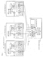
- a multi-processor system 10 shown in Fig. 1 is a system where the access monitoring method and device for shared memory according to the present invention are applied to the prior art star type multi-processor system shown in Fig.12.
- the bus interface 110 within the shared memory board 100 has, in addition to the arrangement shown in Fig.12, a packet receiver/processor 111 receiving a request packet which requests an acquisition or a release of an access right to the shared memory SM from an arbitrary request source processor among the processors 210_1-210_n, acquiring or releasing the access right of the request source processor, and producing generation instructions of an answer packet indicating the acquisition or release of the access right, and a answer packet generator 112 generating the answer packet upon receiving the answer packet generation instructions and broadcasting the answer packet to all of the processors 210_1-210_n.
- the bus interface 220_1-220_n within the processor boards 200_1-200_n respectively have request packet generators 221_1-221_n (hereinafter, occasionally represented by a reference numeral 221) generating the request packet to be transmitted to the shared memory board 100 side, and packet determining portions 222_1.222_n (hereinafter, occasionally represented by a reference numeral 222) receiving the answer packet to be determined.
- request packet generators 221_1-221_n hereinafter, occasionally represented by a reference numeral 221
- packet determining portions 222_1.222_n hereinafter, occasionally represented by a reference numeral 222
- bus interface 110 is configured by being divided into the packet receiver/processor 111 and the answer packet generator 112, both of them may be configured as a single function block. In this case, the following description can be similarly applied.
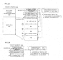
- the shared memory SM is divided, as shown in Fig.2A, into a data area AR1 storing data read or written by the processor 210 and an area AR2 of exclusive control information to the data area AR1.
- the data area AR1 is divided per range of addresses "0"-"x" and has "m+1" units of data blocks D0.Dm whose addresses are "B0-0"-"B0-x", "B1-0"-"B1-x", "B2-0"-"B2-x", ⁇ , and "Bm-0"-Bm-x".
- exclusive control information IO-Im whose addresses are A0, A1, A2, ⁇ , and Am are provided respectively corresponding to the data blocks D0-Dm.
- the exclusive control information includes an access right display bit b1 indicating a status of an acquisition "1" (acquisition completion) or a release "0" (release completion) of the access right to corresponding data block, and a display bit b2 displaying an ID (identifier) of a processor having acquired the access right.
- the cache memory CM includes, as shown in Fig.2B, an area identical to the exclusive control information area AR2 of the shared memory SM.
- FIG.1 An operation of the multi-processor system 10 shown in Fig.1 will be described.
- an operation example (1) where the shared memory SM and the cache memory CM have the same arrangement as shown in Figs.2A and 2B will be described referring to Figs.3, 4A, 4B, 5A, 5B, and 6-8.
- an operation example (2) where the arrangement of the shared memory SM has an arrangement (Fig.9) different from Fig.2A will be described referring to Figs.9 and 10.
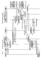
- the processor 210_1 which requests the access to the data block D2 provides, as shown in Fig.3, an access right acquisition request to the request packet generator 221_1 forming the bus interface 220_1 (at step S1).
- the request packet generator 221_1 having received the access right acquisition request generates a request packet RP as described below (at step S2).
- the request packet generator 221_1 sets an access right acquisition request RQ1 shown in Fig.4B, the address A2 of the exclusive control information 12 corresponding to the data block D2, and "210_1", respectively to a request type RP1, address information RP2, and a request source processor ID RP4 in the request packet RP shown in Fig.4A.
- the request packet generator 221_1 transmits the request packet RP generated to the bus interface 110 within the shared memory board 100 (at step S3).
- the packet receiver/processor 111 forming the interface 110 and having received the request packet RP extracts the request type RP1 from the request packet RP for the determination (at step S4).
- the packet receiver/processor 111 refers to the access right display bit b1 in the exclusive control information 12 designated by the address A2 set in the address information RP2 (at step S5).
- the packet receiver/processor 111 determines whether or not the access right display bit b1 indicates the access right release status "0" (at step S6). As a result, when determining that the access right display bit b1 indicates the access right release status "0", the packet receiver/processor 111 updates the access right display bit b1 to the access right acquisition status "1", and sets the processor ID display bit b2 with "210_1" (at step S7).
- the packet receiver/processor 111 can have the processor 210_1 acquire the access right to the data block D2.
- the packet receiver/processor 111 provides generation instructions of an answer packet AP indicating the acquisition of the access right to the data block D2 by the processor 210_1 to the answer packet generator 112 (at step S8).
- the answer packet generator 112 having received the instructions generates the answer packet AP as described below (at step S9).
- the answer packet generator 112 sets an access right acquisition ACK1 shown in Fig.5B, the address A2, and "210_1", respectively to a response type AP1, address information AP2, and a request source processor ID AP4 in the answer packet AP shown in Fig.5A.
- the answer packet generator 112 broadcasts the answer packet AP generated to the bus interfaces 220_1-220_n within all of the processor boards 200_1-200_n (at step S10).
- the packet determining portions 222_1-222_n forming the bus interfaces 220_1-220_n and having received the answer packet AP broadcast respectively extract the response type AP1 from the answer packet AP for the determination (at steps S11_1-S11_n).
- the, packet determining portions 222-1-222-n update to the access right acquisition status "1" the access right display bit b1 of the exclusive control information 12 in the cache memories CM1-CMn designated by the address A2 set in the address information AP2, and set the processor ID display bit b2 with "210_1" set in the request source processor ID AP4 (at steps S12_1-S12_n).
- Each of the packet determining portions 222_1-222_n determines whether or not the processor ID set in the request source processor ID AP4 coincides with its own processor ID. In this example, only the packet determining portion 222_1 determines that both processor IDs are coincident, and transfers the answer packet AP to the processor 210_1 (at step S13).
- the processor 210_1 having received the answer packet AP recognizes that the access right to the data block D2 is acquired, and performs the data read or write as will be described later referring to Fig.7 or 8 (at step S41 or S61).
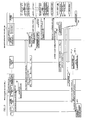
- the processor 210_1 having completed the data read or write provides, as shown in Fig.6, an access right release request to the request packet generator 221_1 in order to release the access right to the data block D2 (at step S21).
- the request packet generator 221_1 having received the request generates the request packet RP as described below (at step S22).
- the request packet generator 221_1 sets an access right release request RQ2 shown in Fig.4B, the address A2 of the exclusive control information 12 corresponding to the data block D2, and "210_1", respectively to the request type RP1, the address information RP2, and the request source processor ID RP4 in the request packet RP.
- the request packet generator 221_1 transmits the request packet RP generated to the packet receiver/processor 111 (at step S23).
- the packet receiver/processor 111 having received the request packet RP extracts the request type RP1 from the request packet RP for the determination (at step S24). As a result, when determining that the access right release request RQ2 is set in the request type RP1, the packet receiver/processor 111 refers to the access right display bit b1 and the processor ID display bit b2 in the exclusive control information 12 designated by the address A2 set in the address information RP2 (at step S25).
- the packet receiver/processor 111 determines whether or not the access right display bit b1 and the processor ID display bit b2 respectively indicate the access right acquisition status "1" and "210_1” having been set in the request source processor ID RP4 (at step S26). As a result, when determining that the access right display bit b1 and the processor ID display bit b2 respectively indicate the access right acquisition status "1" and "210_1", the packet receiver/processor 111 updates the access right display bit b1 to the access right release status "0", and deletes "210_1” having been set in the processor ID display bit b2 (at step S27).
- the packet receiver/processor 111 can release the access right to the data block D2 having been acquired by the processor 210_1.
- the packet receiver/processor 111 provides generation instructions of the answer packet AP indicating the release of the access right to the data block D2 by the processor 210_1 to the answer packet generator 112 (at step S28).
- the answer packet generator 112 having received the instructions generates the answer packet AP as described below (at step S29).
- the answer packet generator 112 sets an access right release ACK2 shown in Fig.5B, the address A2, and "210_1", respectively to the response type AP1, the address information AP2, and the request source processor ID AP4 in the answer packet AP.
- the answer packet generator 112 broadcasts the answer packet AP generated to all of the packet determining portions 222_1-222_n (at step S30):
- the packet determining portions 222_1-222_n having received the answer packet AP broadcast respectively extract the response type AP1 from the answer packet AP for the determination (at steps S31_1-S31_n).
- the packet determining portions 222_1-222_n update to the access right release status "0" the access right display bit b1 of the exclusive control information 12 in the cache memories CM1-CMn designated by the address A2 set in the address information AP2, and delete "210_1" set in the processor ID display bit b2 (at steps S32_1-S32_n).
- the processor 210_1 having requested the release of the access right to the data block D2 can directly update the cache memory CM1 upon the request.
- the cache memory CM1 when the cache memory CM1 is directly updated, the content of the cache memory CM1 may not coincide with the contents of the cache memories CM2-CMn within the other processors 210_2-210_n and the shared memory SM due to influences of loss or the like of the request packet RP or the answer packet AP due to a transmission failure of the serial bus SB. Therefore, the processor 210_1 (packet determining portion 222_1) updates the cache memory CM1 after the determination of the above-mentioned step S31_1.
- the processor 210_1 having acquired the access right to the data block D2 provides, as shown in Fig.7, a data read request from a desired address in the data block D2, e.g. the address "B2-0" to the request packet generator 221_1 (at step S41).
- the request packet generator 221_1 having received the data read request generates the request packet RP as described below (at step S42).
- the request packet generator 221_1 sets a data read request RQ3 shown in Fig.4B, the address "B2-0", and "210_1", respectively to the request type RP1, the address information RP2, and the request source processor ID RP4 in the request packet RP.
- the request packet generator 221_1 transmits the request packet RP generated to the packet receiver/processor 111 (at step S43).
- the packet receiver/processor 111 having received the request packet RP extracts the request type RP1 from the request packet RP for the determination (at step S44). As a result, when determining that the data read request RQ3 is set in the request type RP1, the packet receiver/processor 111 reads data "DT2-0" from an area designated by the address "B2-0" set in the address information RP2 (at step S45).
- the packet receiver/processor 111 provides generation instructions of the answer packet AP set with the data "DT2-0" read to the answer packet generator 112 (at step S46).
- the answer packet generator 112 having received the instructions generates the answer packet AP as described below (at step S47).
- the answer packet generator 112 sets a data read ACK3 shown in Fig. 5B, the address "B2-0”, the data "DT2-0”, and “210_1", respectively to the response, type AP1, the address information AP2, the data AP3, and the request source processor ID AP4 in the answer packet AP.
- the answer packet generator 112 transmits the answer packet AP generated only to the packet determining portion 222_1 (at step S48).
- the packet determining portion 222_1 having received the answer packet AP extracts the response type AP1 from the answer packet AP for the determination (at step S49).
- the packet determining portion 222_1 transfers the answer packet AP to the processor 210_1 (at step S50).
- the processor 210_1 having received the answer packet AP acquires the data "DT2-0" from the data AP3 in the answer packet AP (at step S51).
- the processor 210_1 having acquired the access right to the data block D2 provides, as shown in Fig.8, a data write request of desired data DTy to a desired address in the data block D2, e.g. the address "B2-0" to the request packet generator 221_1 (at step S61).
- the request packet generator 221_1 having received the data write request generates the request packet RP as described below (at step S62).
- the request packet generator 221_1 sets a data write request RQ4 shown in Fig.4B, the address "B2-0", the data DTy, and "210_1", respectively to the request type RP1, the address information RP2, the data RP3, and the request source processor ID RP4 in the request packet RP.
- the request packet generator 221_1 transmits the request packet RP generated to the packet receiver/processor 111 (at step S63).
- the packet receiver/processor 111 having received the request packet RP extracts the request type RP1 from the request packet RP for the determination (at step 864). As a result, when determining that the data write request RQ4 is set in the request type RP1, the packet receiver/processor 111 writes in an area designated by the address "B2-0" set in the address information RP2 the data DTy set in the data RP3 in the request packet RP (at step S65).
- the answer packet AP is not transmitted/received between the shared memory board 100 and the processor board 200 upon the data read, and the processor 210 regards that the execution of the data write is completed when performing the data write request indicated at the above-mentioned step S61.
- a shared memory SM shown in Fig.9 is different from the arrangement (1) of the shared memory shown in Fig.2A in that the data blocks D0-Dm are respectively divided according to addresses B0, B1, B2, B2; ⁇ , and Bm.
- each of the exclusive control information I0-Im is provided, in the same way as the above-mentioned arrangement (1) of the shared memory, corresponding to each of the data blocks D0-Dm, and includes the access right display bit b1 and the processor ID display bit b2.
- the access right acquisition operation example shown in Fig.10 is different from the access right acquisition operation example (1) shown in Fig.3 only in processes of steps S70-573.
- the packet receiver/processor 111 having had the processor 210_1, acquire the access right to the data block D2 reads data DT2 from the data block D2 corresponding to the exclusive control information I2 designated by the address A2 set in the address information RP2 in the request packet RP (at step S70).
- the packet receiver/processor 111 provides instructions for setting the data DT2 read with the acquisition of the access right to the answer packet AP to the answer packet generator 112 (at step S71).
- the answer packet generator 112 having received the instructions sets, in the same way as the above-mentioned access right acquisition operation example (1), to the response type AP1, the address information AP2, and the request source processor ID AP4 in the answer packet AP the access right acquisition ACK1, the address A2, and "210_1" respectively, and sets the data DT2 to the data AP3 which is not used in the above-mentioned access right acquisition operation example (1) (at step S72).
- the answer packet in which the data DT2 is set is to be broadcast to all of the packet determining portions 222_1-222_n.
- the processor 210_1 to which the answer packet AP has been transferred acquires the data DT2 from the data AP3 in the answer packet AP (at step S73).
- the processor 210_1 can acquire the data DT2 stored in the data block D2 without performing the data read request indicated at the step 41 of Fig.7 by concurrently performing the access right acquisition and the data read. It is to be noted that when performing the data write in the data block D2, the processor 210_1 has only to discard the data DT2 acquired and to perform a write request of desired data in the same way as the step S61 of Fig.8:
Landscapes
- Engineering & Computer Science (AREA)
- Theoretical Computer Science (AREA)
- Software Systems (AREA)
- Physics & Mathematics (AREA)
- General Engineering & Computer Science (AREA)
- General Physics & Mathematics (AREA)
- Multi Processors (AREA)
- Memory System Of A Hierarchy Structure (AREA)
- Memory System (AREA)
Applications Claiming Priority (1)
| Application Number | Priority Date | Filing Date | Title |
|---|---|---|---|
| JP2006223299A JP2008046969A (ja) | 2006-08-18 | 2006-08-18 | 共有メモリのアクセス監視方法及び装置 |
Publications (2)
| Publication Number | Publication Date |
|---|---|
| EP1895413A2 true EP1895413A2 (de) | 2008-03-05 |
| EP1895413A3 EP1895413A3 (de) | 2009-09-30 |
Family
ID=38835067
Family Applications (1)
| Application Number | Title | Priority Date | Filing Date |
|---|---|---|---|
| EP07015874A Withdrawn EP1895413A3 (de) | 2006-08-18 | 2007-08-13 | Zugangsüberwachungsverfahren und Vorrichtung für gemeinsamen Speicher |
Country Status (3)
| Country | Link |
|---|---|
| US (1) | US20080047005A1 (de) |
| EP (1) | EP1895413A3 (de) |
| JP (1) | JP2008046969A (de) |
Cited By (1)
| Publication number | Priority date | Publication date | Assignee | Title |
|---|---|---|---|---|
| EP2328095A4 (de) * | 2008-09-03 | 2012-11-07 | Hitachi Automotive Systems Ltd | Steuersoftware für verteilte steuerung sowie elektronische steuerungsvorrichtung |
Families Citing this family (11)
| Publication number | Priority date | Publication date | Assignee | Title |
|---|---|---|---|---|
| JP5022330B2 (ja) * | 2008-09-22 | 2012-09-12 | エヌイーシーコンピュータテクノ株式会社 | リクエスト発行ノード、リクエスト受信ノード、システム、及び制御方法 |
| JP5395838B2 (ja) | 2011-03-25 | 2014-01-22 | 株式会社東芝 | マルチコアシステム |
| CN105793830B (zh) | 2013-12-26 | 2019-12-24 | 英特尔公司 | 一种在节点之间共享存储器和i/o服务的装置、方法、系统 |
| KR102400014B1 (ko) * | 2014-12-26 | 2022-05-20 | 삼성전자주식회사 | 이동 단말의 데이터 브로드캐스팅을 이용한 서비스 제공 방법 및 장치 |
| KR101716862B1 (ko) * | 2016-10-04 | 2017-03-15 | (주)볼트마이크로 | 영상데이터 관리 장치 및 방법 |
| US20180285262A1 (en) * | 2017-03-31 | 2018-10-04 | Intel Corporation | Techniques for shared virtual memory access protection |
| CN108628621A (zh) * | 2018-03-05 | 2018-10-09 | 深圳市鼎阳科技有限公司 | 一种从设备的固件升级方法及固件升级的从设备、系统 |
| KR102833251B1 (ko) * | 2020-12-02 | 2025-07-14 | 주식회사 텔레칩스 | Otp 메모리에 대한 프로세서들의 접근 제어 방법 및 이를 구현한 데이터 처리 시스템 |
| US20230359376A1 (en) * | 2022-05-08 | 2023-11-09 | Samsung Electronics Co., Ltd. | Systems, methods, and apparatus for managing device memory and programs |
| CN115455397B (zh) * | 2022-10-28 | 2023-03-21 | 湖北芯擎科技有限公司 | 一种输入输出接口控制方法及系统 |
| CN117609114B (zh) * | 2023-11-10 | 2024-09-03 | 北京智芯微电子科技有限公司 | 多核处理器数据共享控制方法、装置、存储模块及芯片 |
Citations (3)
| Publication number | Priority date | Publication date | Assignee | Title |
|---|---|---|---|---|
| JP2000267815A (ja) | 1999-03-17 | 2000-09-29 | Hitachi Ltd | ディスクアレイ制御装置 |
| JP2000267816A (ja) | 1999-03-17 | 2000-09-29 | Hitachi Ltd | ディスクアレイ制御装置 |
| WO2001016738A2 (en) | 1999-08-31 | 2001-03-08 | Times N Systems, Inc. | Efficient page ownership control |
Family Cites Families (9)
| Publication number | Priority date | Publication date | Assignee | Title |
|---|---|---|---|---|
| US4410944A (en) * | 1981-03-24 | 1983-10-18 | Burroughs Corporation | Apparatus and method for maintaining cache memory integrity in a shared memory environment |
| US5142676A (en) * | 1988-12-28 | 1992-08-25 | Gte Laboratories Incorporated | Separate content addressable memories for storing locked segment addresses and locking processor identifications for controlling access to shared memory |
| JPH0664567B2 (ja) * | 1989-12-25 | 1994-08-22 | 株式会社日立製作所 | 多重プロセッサシステム |
| JPH04362755A (ja) * | 1991-06-10 | 1992-12-15 | Nec Corp | 共用型拡張記憶試験方式 |
| US5584017A (en) * | 1991-12-19 | 1996-12-10 | Intel Corporation | Cache control which inhibits snoop cycles if processor accessing memory is the only processor allowed to cache the memory location |
| JP3093609B2 (ja) * | 1995-07-27 | 2000-10-03 | エヌイーシーソフト株式会社 | キャッシュメモリの記憶一致制御装置及び方法 |
| JPH09231124A (ja) * | 1996-02-20 | 1997-09-05 | Ricoh Co Ltd | メモリロック装置及びメモリロック方法 |
| JP2924786B2 (ja) * | 1996-04-26 | 1999-07-26 | 日本電気株式会社 | 疎結合多重計算機システムにおける共有ファイルの排他制御システム、排他制御方法、および排他制御プログラムを記憶する媒体 |
| US6195724B1 (en) * | 1998-11-16 | 2001-02-27 | Infineon Technologies Ag | Methods and apparatus for prioritization of access to external devices |
-
2006
- 2006-08-18 JP JP2006223299A patent/JP2008046969A/ja active Pending
-
2007
- 2007-08-13 EP EP07015874A patent/EP1895413A3/de not_active Withdrawn
- 2007-08-14 US US11/838,334 patent/US20080047005A1/en not_active Abandoned
Patent Citations (3)
| Publication number | Priority date | Publication date | Assignee | Title |
|---|---|---|---|---|
| JP2000267815A (ja) | 1999-03-17 | 2000-09-29 | Hitachi Ltd | ディスクアレイ制御装置 |
| JP2000267816A (ja) | 1999-03-17 | 2000-09-29 | Hitachi Ltd | ディスクアレイ制御装置 |
| WO2001016738A2 (en) | 1999-08-31 | 2001-03-08 | Times N Systems, Inc. | Efficient page ownership control |
Cited By (1)
| Publication number | Priority date | Publication date | Assignee | Title |
|---|---|---|---|---|
| EP2328095A4 (de) * | 2008-09-03 | 2012-11-07 | Hitachi Automotive Systems Ltd | Steuersoftware für verteilte steuerung sowie elektronische steuerungsvorrichtung |
Also Published As
| Publication number | Publication date |
|---|---|
| EP1895413A3 (de) | 2009-09-30 |
| US20080047005A1 (en) | 2008-02-21 |
| JP2008046969A (ja) | 2008-02-28 |
Similar Documents
| Publication | Publication Date | Title |
|---|---|---|
| US20080047005A1 (en) | Access monitoring method and device for shared memory | |
| US5535340A (en) | Method and apparatus for maintaining transaction ordering and supporting deferred replies in a bus bridge | |
| KR100496116B1 (ko) | 멀티프로세서 장치 | |
| CN108989432B (zh) | 用户态的文件发送方法、文件接收方法和文件收发装置 | |
| JP2002528814A (ja) | 分散型トランザクション処理システムと方法 | |
| JP2009211368A (ja) | キャッシュメモリ及びベクトル処理装置並びにベクトルデータ整列方法 | |
| EP2845110B1 (de) | Reflektierende speicherbrücke für externe rechnerknoten | |
| CN116107771B (zh) | 缓存状态记录方法、数据访问方法及相关装置、设备 | |
| CN111124255A (zh) | 数据存储方法、电子设备和计算机程序产品 | |
| US7216205B2 (en) | Cache line ownership transfer in multi-processor computer systems | |
| US6678722B1 (en) | Interprocessor communication system for parallel processing | |
| US20020089940A1 (en) | Duplexing apparatus and method in large scale system | |
| CN117201518B (zh) | 数据的传输方法、系统、装置、存储介质和电子设备 | |
| US20160357780A1 (en) | Hierarchical file block variant tracker apparatus coupled to a Librarian and to a remote file service | |
| JP3080552B2 (ja) | 複合計算機システムのメモリ装置 | |
| US7529857B2 (en) | Data processing apparatus and data transfer control method | |
| JP2007226641A (ja) | 情報処理装置、キャッシュ制御方法及びプログラム | |
| JP2002024007A (ja) | プロセッサシステム | |
| JP2001167068A (ja) | メモリアクセス方法及びマルチプロセッサシステム | |
| CN118363901B (zh) | PCIe设备、电子组件及电子设备 | |
| JP2001318905A (ja) | ディスク共有型分散サーバシステム | |
| US7051148B2 (en) | Data transmission sequencing method associated with briding device and application system | |
| US20090031101A1 (en) | Data processing system | |
| US20250021256A1 (en) | Hierarchical File Block Variant Tracking | |
| CN119668514B (zh) | 一种共享集群的资源接管方法、装置、设备及介质 |
Legal Events
| Date | Code | Title | Description |
|---|---|---|---|
| PUAI | Public reference made under article 153(3) epc to a published international application that has entered the european phase |
Free format text: ORIGINAL CODE: 0009012 |
|
| AK | Designated contracting states |
Kind code of ref document: A2 Designated state(s): AT BE BG CH CY CZ DE DK EE ES FI FR GB GR HU IE IS IT LI LT LU LV MC MT NL PL PT RO SE SI SK TR |
|
| AX | Request for extension of the european patent |
Extension state: AL BA HR MK YU |
|
| PUAL | Search report despatched |
Free format text: ORIGINAL CODE: 0009013 |
|
| AK | Designated contracting states |
Kind code of ref document: A3 Designated state(s): AT BE BG CH CY CZ DE DK EE ES FI FR GB GR HU IE IS IT LI LT LU LV MC MT NL PL PT RO SE SI SK TR |
|
| AX | Request for extension of the european patent |
Extension state: AL BA HR MK RS |
|
| 17P | Request for examination filed |
Effective date: 20100305 |
|
| AKX | Designation fees paid |
Designated state(s): DE FR GB |
|
| STAA | Information on the status of an ep patent application or granted ep patent |
Free format text: STATUS: THE APPLICATION IS DEEMED TO BE WITHDRAWN |
|
| 18D | Application deemed to be withdrawn |
Effective date: 20120301 |