EP1895540A1 - Memoire a semi-conducteurs non volatile et procede d'ecriture pour une telle memoire - Google Patents
Memoire a semi-conducteurs non volatile et procede d'ecriture pour une telle memoire Download PDFInfo
- Publication number
- EP1895540A1 EP1895540A1 EP05750964A EP05750964A EP1895540A1 EP 1895540 A1 EP1895540 A1 EP 1895540A1 EP 05750964 A EP05750964 A EP 05750964A EP 05750964 A EP05750964 A EP 05750964A EP 1895540 A1 EP1895540 A1 EP 1895540A1
- Authority
- EP
- European Patent Office
- Prior art keywords
- resistance
- memory element
- value
- voltage
- current
- Prior art date
- Legal status (The legal status is an assumption and is not a legal conclusion. Google has not performed a legal analysis and makes no representation as to the accuracy of the status listed.)
- Withdrawn
Links
Images







Classifications
-
- G—PHYSICS
- G11—INFORMATION STORAGE
- G11C—STATIC STORES
- G11C13/00—Digital stores characterised by the use of storage elements not covered by groups G11C11/00, G11C23/00, or G11C25/00
- G11C13/0002—Digital stores characterised by the use of storage elements not covered by groups G11C11/00, G11C23/00, or G11C25/00 using resistive RAM [RRAM] elements
- G11C13/0021—Auxiliary circuits
- G11C13/003—Cell access
-
- G—PHYSICS
- G11—INFORMATION STORAGE
- G11C—STATIC STORES
- G11C11/00—Digital stores characterised by the use of particular electric or magnetic storage elements; Storage elements therefor
- G11C11/56—Digital stores characterised by the use of particular electric or magnetic storage elements; Storage elements therefor using storage elements with more than two stable states represented by steps, e.g. of voltage, current, phase, frequency
- G11C11/5685—Digital stores characterised by the use of particular electric or magnetic storage elements; Storage elements therefor using storage elements with more than two stable states represented by steps, e.g. of voltage, current, phase, frequency using storage elements comprising metal oxide memory material, e.g. perovskites
-
- G—PHYSICS
- G11—INFORMATION STORAGE
- G11C—STATIC STORES
- G11C13/00—Digital stores characterised by the use of storage elements not covered by groups G11C11/00, G11C23/00, or G11C25/00
- G11C13/0002—Digital stores characterised by the use of storage elements not covered by groups G11C11/00, G11C23/00, or G11C25/00 using resistive RAM [RRAM] elements
- G11C13/0007—Digital stores characterised by the use of storage elements not covered by groups G11C11/00, G11C23/00, or G11C25/00 using resistive RAM [RRAM] elements comprising metal oxide memory material, e.g. perovskites
-
- G—PHYSICS
- G11—INFORMATION STORAGE
- G11C—STATIC STORES
- G11C13/00—Digital stores characterised by the use of storage elements not covered by groups G11C11/00, G11C23/00, or G11C25/00
- G11C13/0002—Digital stores characterised by the use of storage elements not covered by groups G11C11/00, G11C23/00, or G11C25/00 using resistive RAM [RRAM] elements
- G11C13/0021—Auxiliary circuits
- G11C13/0069—Writing or programming circuits or methods
-
- G—PHYSICS
- G11—INFORMATION STORAGE
- G11C—STATIC STORES
- G11C13/00—Digital stores characterised by the use of storage elements not covered by groups G11C11/00, G11C23/00, or G11C25/00
- G11C13/0002—Digital stores characterised by the use of storage elements not covered by groups G11C11/00, G11C23/00, or G11C25/00 using resistive RAM [RRAM] elements
- G11C13/0021—Auxiliary circuits
- G11C13/0069—Writing or programming circuits or methods
- G11C2013/0083—Write to perform initialising, forming process, electro forming or conditioning
-
- G—PHYSICS
- G11—INFORMATION STORAGE
- G11C—STATIC STORES
- G11C13/00—Digital stores characterised by the use of storage elements not covered by groups G11C11/00, G11C23/00, or G11C25/00
- G11C13/0002—Digital stores characterised by the use of storage elements not covered by groups G11C11/00, G11C23/00, or G11C25/00 using resistive RAM [RRAM] elements
- G11C13/0021—Auxiliary circuits
- G11C13/0069—Writing or programming circuits or methods
- G11C2013/009—Write using potential difference applied between cell electrodes
-
- G—PHYSICS
- G11—INFORMATION STORAGE
- G11C—STATIC STORES
- G11C2213/00—Indexing scheme relating to G11C13/00 for features not covered by this group
- G11C2213/30—Resistive cell, memory material aspects
- G11C2213/31—Material having complex metal oxide, e.g. perovskite structure
-
- G—PHYSICS
- G11—INFORMATION STORAGE
- G11C—STATIC STORES
- G11C2213/00—Indexing scheme relating to G11C13/00 for features not covered by this group
- G11C2213/30—Resistive cell, memory material aspects
- G11C2213/32—Material having simple binary metal oxide structure
-
- G—PHYSICS
- G11—INFORMATION STORAGE
- G11C—STATIC STORES
- G11C2213/00—Indexing scheme relating to G11C13/00 for features not covered by this group
- G11C2213/30—Resistive cell, memory material aspects
- G11C2213/34—Material includes an oxide or a nitride
-
- G—PHYSICS
- G11—INFORMATION STORAGE
- G11C—STATIC STORES
- G11C2213/00—Indexing scheme relating to G11C13/00 for features not covered by this group
- G11C2213/70—Resistive array aspects
- G11C2213/74—Array wherein each memory cell has more than one access device
-
- G—PHYSICS
- G11—INFORMATION STORAGE
- G11C—STATIC STORES
- G11C2213/00—Indexing scheme relating to G11C13/00 for features not covered by this group
- G11C2213/70—Resistive array aspects
- G11C2213/75—Array having a NAND structure comprising, for example, memory cells in series or memory elements in series, a memory element being a memory cell in parallel with an access transistor
-
- G—PHYSICS
- G11—INFORMATION STORAGE
- G11C—STATIC STORES
- G11C2213/00—Indexing scheme relating to G11C13/00 for features not covered by this group
- G11C2213/70—Resistive array aspects
- G11C2213/79—Array wherein the access device being a transistor
Definitions
- the present invention relates to a nonvolatile semiconductor memory device, more specifically, a nonvolatile semiconductor memory device using a resistance memory element having a plurality of resistance states of different resistance values and a method of writing into the same.
- RRAM Resistance Random Access Memory
- the RRAM uses a resistance memory element which has a plurality of resistance states of different resistance values, which are changed by electric stimulations applied from the outside and whose high resistance state and low resistance state are corresponded to, e.g., information "0" and "1" to be used as a memory element.
- the RRAM highly potentially has high speed, large capacities, low electric power consumption, etc. and is considered prospective.
- the resistance memory element has a resistance memory material whose resistance states are changed by the application of voltages sandwiched between a pair of electrodes.
- oxide materials containing transition metals are known and, depending on the electric characteristics, can be classified largely in two.
- the RRAM using such bipolar material is disclosed in, e.g., Patent Reference 1, Non-Patent Reference 1 and Non-Patent Reference 2.
- the other uses voltages of the same polarity so as to change the resistance state between the high resistance state and the low resistance state and includes oxides of single transition metals, etc., e.g., NiO x , TiO x .
- the RRAM using such unipolar material is disclosed in, e.g., Non-Patent Reference 3.
- the multiple-valued memory is different from the usual binary memory, in which one memory cell can take either state of "0" and "1" but is a memory element in which one memory cell can take three or more states.
- Patent Reference 1 and Non-Patent Reference 2 disclose that when the amplitude width or the width of the voltage pulse to be applied to bipolar resistance memory materials is varied, corresponding to this, the absolute value of resistance of the low resistance state is varied.
- the possibility of forming a multiple-valued memory by making use of not only two resistances, a high resistance and a low resistance, but also low resistance states of middle resistances between both resistances and others is also disclosed.
- An object of the present invention is to provide a nonvolatile semiconductor memory device using a resistance memory element which memorizes a plurality of resistance states of different resistance value and a method of writing into the same which can realize two or more resistance states with good reproducibility.
- Another object of the present invention is to provide a nonvolatile semiconductor memory device and the method of writing the same which, when the resistance memory element is switched from the high resistance state to the low resistance state, can prevent the flow of large current to the element.
- a method of writing into a nonvolatile semiconductor memory device including a resistance memory element which memorizes a high resistance state and a low resistance state and switches between the high resistance state and the low resistance state by an application of a voltage, when the voltage is applied to the resistance memory element to thereby switch from the high resistance state to the low resistance state, a value of a current to flow in the resistance memory element being limited to thereby memorize the low resistance state of a low resistance value corresponding to the limited value of the current.
- a nonvolatile semiconductor memory device comprising; a resistance memory element which memorizes a high resistance state and a low resistance state and switches between the high resistance state and the low resistance state by an application of a voltage; a variable resistor serially connected to the resistance memory element; and a current limitation circuit which, when the voltage is applied to the resistance memory element to switch from the high resistance state to the low resistance stage, a value of a current to flow in the resistance memory element being limited to memorize in the resistance memory element the low resistance state of a low resistance value corresponding to the limited value of the current.
- a nonvolatile semiconductor memory device comprising: a plurality of memory cells arranged in a matrix, each including a resistance memory element which memorizes a high resistance state and a low resistance state and switches between the high resistance state and the low resistance state by an application of a voltage, and a select transistor having one terminal serially connected to one terminal of the resistance memory element; a plurality of first signal lines parallelly extended in a first direction and each connected to gate electrodes of the select transistors of the memory cells arranged in the first direction; a plurality of second signal lines parallelly extended in a second direction intersecting the first direction and each connected to the other terminals of the resistance memory elements of the memory cells arranged in the second direction; a plurality of third signal lines parallelly extended in the first direction and each connected to the other terminals of the select transistors of the memory cells arranged in the first direction; variable resistors serially connected to the other terminals of the resistance memory elements; and a current limitation circuit which, when a voltage is
- a resistor is serially connected to the resistance memory element to thereby prevent the flow of large current in the resistance memory element, whereby the breakage of the resistance memory element due to the flow of large current can be prevented.
- the resistance value of the resistance memory element in the low resistance state can be controlled by resistance values of the resistance element.
- the nonvolatile semiconductor memory device and method of writing into the same according to a first embodiment of the present invention will be explained with reference to FIGs. 1 to 9 .
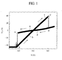
- FIG. 1 is a graph showing the current-voltage characteristics of the resistance memory element using a bipolar resistance memory material.
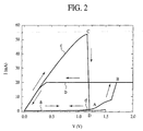
- FIG. 2 is a graph showing the current-voltage characteristics of the resistance memory element using a unipolar resistance memory material.
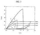
- FIG. 3 is a graph showing the current-voltage characteristics of the unipolar resistance memory material with changing the set value of the current limiter.
- FIG. 4 is a graph showing the current-voltage characteristics of the resistance memory element using the unipolar resistance memory material, which explains the forming process thereof.
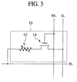
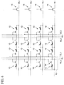
- FIGs. 5 and 6 are circuit diagrams showing the structure of the nonvolatile semiconductor memory device according to the present embodiment.
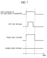
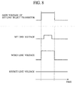
- FIGs. 7 and 8 are time charts showing the method of writing into the nonvolatile semiconductor memory device according to the present embodiment.
- FIG. 9 is a time chart showing the method of reading the nonvolatile semiconductor memory device according to the present embodiment.
- the resistance memory element includes the resistance memory material sandwiched between a pair of electrodes.
- Many of the resistance memory material are oxide materials containing transition metals, and the resistance memory material is divided largely in two, depending on differences in the electric characteristics.
- One of them uses voltages of different polarities so as to change the resistance states between the high resistance state and the low resistance state and includes SrTiO 3 and SrZrO 3 doped with a trace of an impurity, such as chrome (Cr) or others, and Pr 1-x Ca x MnO 3 and La 1-x Ca x MnO 3 , etc., which exhibit CMR (Colossal Magneto-Resistance).
- an impurity such as chrome (Cr) or others
- Pr 1-x Ca x MnO 3 and La 1-x Ca x MnO 3 , etc. which exhibit CMR (Colossal Magneto-Resistance).
- Such resistance memory material which requires voltages of different polarities so as to rewrite the resistance state will be hereinafter called the bipolar resistance memory material.
- the other of them is materials which require voltages of the same polarity so as to change the resistance states between the high resistance state and the low resistance state and includes oxides, etc., containing a single transition metal, such as NiO x and TiO x .
- Such resistance memory materials which require voltages of the same polarity for rewriting the resistance states will be hereinafter called the unipolar resistance memory material.
- FIG. 1 is a graph of the current-voltage characteristics of the resistance memory element using the bipolar resistance memory material and is disclosed in Non-Patent Reference 1. This graph is of the resistance memory element using Cr-doped SrZrO 3 , which is the typical bipolar resistance memory material.
- the resistance memory element is in the high resistance state.
- the current flowing at this time changes along the curve "a" in the arrowed direction, and its absolute value gradually increases.
- the applied negative voltage is further increased and exceed about -0.5 V, the resistance memory element switches from the high resistance state to the low resistance state.
- the absolute value of the current abruptly increases, and the current-voltage characteristics transits from the point A to the point B.
- the operation of changing the resistance memory element from the high resistance state to the low resistance state is called "set".
- the current value changes along the curve "c" in the arrowed direction, and its absolute values gradually increases.
- the applied positive voltage further increases and exceeds about 0.5 V, the resistance memory element switches from the low resistance state to the high resistance state.
- the absolute value of the current abruptly decreases, and the current-voltage characteristics transit from the point C to the point D.
- the operation of changing the resistance memory element from the low resistance state to the high resistance state is called "reset".
- the respective resistance states are stable in the range of about ⁇ 0.5 V and can be retained even when the electric power source is turned off. That is, in the high resistance state, when an applied voltage is lower than the absolute value of the voltage at the point A, the current-voltage characteristics changes linearly along the curves "a” and “d”, and the high resistance state is retained. Similarly, in the low resistance state, when an applied voltage is lower than the absolute value of the voltage at the point C, the current-voltage characteristics changes linearly along the curves "b" and "c”, and the low resistance state is retained.
- FIG. 2 is a graph of the current-voltage characteristics of the resistance memory element using the unipolar resistance memory material. This graph is of the resistance memory element using TiO x , which is the typical unipolar resistance memory material.
- the resistance memory element is in the high resistance state.
- the current value at the point B is constantly about 20 mA because of the current limiter for preventing the element from breaking due to abrupt current increases.
- the respective resistance states are stable not more than about 1.0 V and are retained when the electric power is turned off. That is, in the high resistance state, when the applied voltage is below the voltage at the point A, the current-voltage characteristics linearly change along the curve "a", and the high resistance state is retained. Similarly, in the low resistance state, when the applied voltage is below the voltage at the point C, the current-voltage characteristics change along the curve "c", and the low resistance state is retained.
- a current limiter for prohibiting the current of above a prescribed value to the element when the resistance memory element is set at the low resistance state.
- the current limiter can be realized simply by connecting serially to the resistance memory element a resistor having a resistance value which cannot be ignored with respect to a resistance value of the resistance memory element in the low resistance state.
- the inventor of the present application made earnest studies of this current limiter, it has been evident for the first time that a resistance value with the resistance memory element set at the low resistance state can be controlled by a set value of the current limiter.
- a resistance value with the resistance memory element set at the low resistance state can be controlled by a set value of the current limiter.
- FIG. 3 is a graph of the current-voltage characteristics of the resistance memory element with the set value of the current limiter changed to 10 mA, 15 mA and 20 mA.
- the dot line is for the 10 mA
- the one dot chain line is for the 15 mA
- the solid line is for the 20 mA.
- the current-voltage characteristics of the resistance memory element change.
- the set value of the current limiter being 10 mA
- the current value goes on decrease along the curve "a” and returns to the origin.
- the set value of the current limiter being 15 mA
- the current value goes on decrease along the curve "b" steeper than the curve "a” and returns to the origin.
- the set value of the current limiter being 20 mA
- the current value goes on decrease along the curve "c" steeper than the curve "b” and returns to the origin.
- the current value goes on increase along the curve "a"
- the set value of the current limiter being 15 mA
- the current value goes on increase along the curve "b”
- the current value goes on increase along the curve "c"
- the resistance memory element is set at a smaller resistance value as the set value of the current limiter is larger.
- the current value As the applied voltage is further increased, the current value abruptly decreases, and the resistance memory element is reset at the high resistance state. Then, as the applied voltage is decreased, the current value goes on decrease along the curve "d" and returns to the origin.
- the voltage necessary for the reset is, as shown in FIG. 3 , higher as the set value of the current limiter for the setting is higher.
- the set value of the current limiter in setting the resistance memory element at the low resistance state is changed, whereby the resistance value of the resistance memory element in the low resistance state can be controlled.
- the resistance value at this time can be preserved unless the resistance memory element is reset.
- the set value of the current limiter is changed to thereby set the resistance memory element, whereby the resistance memory element can be used a multiple-valued memory.
- the resistance memory element formed of the above-described material cannot have the characteristics shown in FIGs. 1 and 2 in the initial state immediately after the element formation.
- the processing called "forming" is necessary.
- FIG. 4 shows the current-voltage characteristics explaining the forming process of the resistance memory element using the same unipolar resistance memory material as in FIGs. 2 and 3 .
- the element In the initial state immediately after the element has been formed, as shown in FIG. 4 , the element is highly resistive and has a breakdown voltage of about 8 V which is very high. This breakdown voltage is very high in comparison with voltages necessary for the setting and resetting. In the initial state, changes of the resistance state, such as the setting and resetting, do not take place.
- the resistance memory element When a voltage higher than the breakdown voltage is applied in the initial state, as shown in FIG. 4 , the value of the current flowing through the element abruptly increases, that is, the forming of the resistance memory element is made. Such forming is made, whereby the resistance memory element exhibits the current-voltage characteristics shown in FIG. 2 and can switch reversibly between the low resistance state and the high resistance state. Once subjected to the forming, the resistance memory element does not return to the initial state.
- the resistance memory element in the initial state before subjected to the forming has a high resistance value, and this high resistance state might be misunderstood to be the high resistance state after the forming.
- the high resistance state means the high resistance state of the resistance memory element after subjected to the forming
- the low resistance state means the low resistance state of the resistance memory element after subjected to the forming
- the initial state is the state of the resistance memory element before subjected to the forming.
- FIGs. 5 and 6 are circuit diagrams showing the structure of the nonvolatile semiconductor memory device according to the present embodiment.
- a memory cell 10 of the nonvolatile semiconductor memory device includes a resistance memory element 12 and a cell select transistor 14.
- the resistance memory element 12 has one end connected to a bit line BL and the other end connected to the drain terminal of the cell select transistor 14.
- the cell select transistor 14 has the source terminal connected to a source line SL and the gate terminal connected to a word line WL.
- the resistance memory element 12 includes a resistance memory material sandwiched between a pair of electrodes.
- the resistance memory material may be a bipolar resistance memory material or a unipolar resistance memory material.
- the resistance memory material is a unipolar resistance material of, e.g. TiO x .
- FIG. 6 is a circuit diagram of a memory cell array of the memory cells 10 shown in FIG. 5 arranged in a matrix.
- a plurality of memory cells 10 are formed adjacent to each other in the column direction (vertically in the drawing) and in the row direction (horizontally in the drawing).
- a plurality of word lines WL1, /WL1, WL2, /WL2 ... are arranged, forming signal lines common among the memory cells 10 arranged in the column direction.
- source lines SL1, SL2 ... are arranged, forming signal lines common among the memory cells 10 arranged column direction.
- the source lines SL are provided each for two word lines WL.
- bit lines BL1, BL2, BL3, BL4 ... are arranged, forming signal lines common among the memory cells 10 arranged in the row direction.
- bit line select transistor 16 As a variable resistor is connected to each bit line BL.
- a memory cell 10 to be rewritten is a memory cell 10 connected to the word line WL1 and the bit line BL1.
- a prescribed voltage is applied to the gate terminal of the bit line select transistor 16 connected to the bit line BL1 to turn on the bit line select transistor 16 (refer to FIG. 7 ).
- the voltage to be applied to the gate terminal is controlled so that a channel resistance R BS of the bit line select transistor 16 has a value which is sufficiently smaller than a resistance value R H of the resistance memory element 12 in the high resistance state and is not negligible in comparison with a resistance value R L of the resistance memory element 12 in the low resistance state.
- a prescribed voltage is applied to the word line WL1 to turn on the cell select transistor 14 (refer to FIG. 7 ).
- the voltage to be applied to the word line WL1 is controlled so that a channel resistance R CS of the cell select transistor 14 has a value which is negligibly small in comparison with the resistance value R L of the resistance memory element 12 in the low resistance state.
- the source line SL is connected to a reference voltage, e.g., 0 V, which is the ground potential (refer to FIG. 7 ).
- a bias voltage which is the same as a voltage required to set the resistance memory element 12 or a little larger than the voltage is applied (refer to FIG. 7 ).
- a current passage to the source line SL1 via the bit line select transistor 16, the bit line BL1, the resistance memory element 12 and the cell select transistor 14 is formed, and the applied bias voltage is divided to the bit line select transistor 16 and the cell select transistor 14 corresponding to the channel resistance R BS of the bit line select transistor 16 and the channel resistance R cs of the cell select transistor 14.
- the resistance value R H of the resistance memory element 12 is sufficiently large in comparison with the channel resistance R BS of the bit line select transistor 16 and the channel resistance R CS of the cell select transistor, and most of the bias voltage is applied to the resistance memory element 12.
- the resistance memory element 12 is changed from the high resistance state to the low resistance state.
- the channel resistance R BS of the bit line select transistor 16 can be set at an arbitrary value as far as the performance of the bit line select transistor 16 permits, which permits the voltage to be applied to the resistance memory element 12, i.e., the current flowing through the resistance memory element 12 to be set at an arbitrary value by the gate voltage of the bit line select transistor 16.
- the current flowing in the resistance memory element 12 can be limited to a prescribed value by the gate voltage of the bit line select transistor 16, and by this current limitation, the resistance value of the resistance memory element 12 can be controlled.
- the value of the current flowing in the resistance memory element 12 is limited to not more than 10 mA, whereby the resistance memory element 12 has the resistance characteristics indicated by the curve "a”, and the value of the current flowing in the resistance memory element 12 is limited to not more than 15 mA, whereby the resistance memory element 12 has the resistance characteristics indicated by the curve "b", and the value of the current flowing in the resistance memory element 12 is limited to not more than 15 mA, whereby the resistance memory element has the resistance characteristics indicated by the curve "c''.
- the resistance memory element 12 is set anew at the low resistance state of the second resistance value.
- a memory cell 10 to be rewritten is the memory cell 10 connected to the word line WL1 and the bit line BL1.
- a prescribed voltage is applied to the gate terminal of the bit line select transistor 16 connected to the bit line BL1 to turn on the bit line select transistor 16 (refer to FIG. 8 ).
- the voltage to be applied to the gate terminal is controlled so that the channel resistance R BS of the bit line select transistor 16 becomes sufficiently smaller than the resistance value R L of the resistance memory element 12 in the low resistance state.
- a prescribed voltage is applied o the word line WL1 to turn on the cell select transistor 14 (refer to FIG. 8 ).
- the voltage to be applied to the word line WL1 is controlled so that the channel resistance R cs of the cell select transistor 14 becomes sufficiently smaller than the resistance value R L of the resistance memory element 12 in the low resistance state.
- the source line SL1 is connected to a reference potential, e.g., 0 V, which is the ground potential (refer to FIG. 8 ).
- a bias voltage which is the same as or a little larger than the voltage necessary to reset the resistance memory element 12 is applied (refer to FIG. 8 ).
- a current passage to the source line SL1 via the bit line BL1, the resistance memory element 12 and the cell select transistor 14 is formed, and the applied bias voltage is divided to the resistance memory element 12, the bit line select transistor 16 and the cell select transistor 14, corresponding to the resistance value R L of the resistance memory element 12, the channel resistance R BS of the bit line select transistor 16 and the channel resistance R cs of the cell select transistor 14.
- the channel resistance R BS of the bit line select transistor 16, and channel resistance R CS of the cell select transistor 14 are sufficiently smaller than the resistance value R L of the resistance memory element 12, and most of the applied bias voltage is applied to the resistance memory element 12.
- the resistance memory element 12 is changed from the low resistance state to the high resistance state.
- the bias voltage to be applied to the bit line BL must be smaller than a voltage necessary for the setting.
- the gate voltages of these transistors are adjusted so that the channel resistance R BS of the bit line select transistor 16 and the channel resistance R CS of the cell select transistor 14 are sufficiently smaller than the resistance value R L of the resistance memory element 12 while the bias voltage to be applied to the bit line BL is set to be not less than the voltage necessary for the resetting and less than the voltage necessary for the setting.
- the word lines WL and the source lines SL are arranged column direction, and the memory cells 10 connected to one word line (e.g., WL1) are connected to the same source line SL (e.g., SL1).
- a plurality of bit lines BL e.g., BL1 - BL4 are simultaneously driven, whereby a plurality of the memory cells 10 connected to a select word line (e.g., WL1) can be reset at once.
- the memory cell to be read is a memory cell 10 connected to the word line WL1 and the bit line BL1.
- a prescribed voltage is applied to the gate terminal of the bit line select transistor 16 to turn on the bit line select transistor 16 (refer to FIG. 9 ).
- the voltage to be applied to the gate terminal is controlled so that the channel resistance R BS of the bit line select transistor 16 is sufficiently smaller than the resistance value R L of the resistance memory element 12.
- a prescribed voltage is applied to the word line WL1 to turn on the cell select transistor 14 (refer to FIG. 9 ).
- the voltage to be applied to the word line WL is controlled so that the channel resistance R cs of the cell select transistor 14 is sufficiently smaller than the resistance value R L of the resistance memory element 12 in the low resistance state.
- the source line SL1 is connected to a reference potential, e.g., 0 V, which is the ground potential (refer to FIG. 9 ).
- bias voltage is applied to the drain terminal of the bit line select transistor 16 (refer to FIG. 9 ).
- This bias voltage is set in accordance with the memory characteristics given by the lowest current limitation value. That is, the value of the bias voltage is set so that even with the resistance memory element in any resistance state, neither the setting nor the resetting is caused by the applied voltage.
- the bias voltage for reading is set at a voltage which ensures a sufficient margin at a voltage of not more than 0.6 V (e.g., 0.5 V).
- the resistor when the resistance memory element is switched from the high resistance state to the low resistance state, the resistor is serially connected to the resistance memory element to thereby prevent the flow of large current to the resistance memory element, whereby the breakage and degradation of the resistance memory element due to the flow of the large current can be prevented.
- the resistance value of the resistor By the resistance value of the resistor, the resistance value of the resistance memory element in the low resistance state can be controlled.
- the multiple-valued memory can be easily realized.
- the nonvolatile semiconductor memory device and the method of writing into the same according to a second embodiment of the present invention will be explained.
- the same members of the present embodiment as those of the nonvolatile semiconductor memory device, the method of writing into the same and the method of reading the same according to the first embodiment shown in FIGs. 1 to 9 are represented by the same reference numbers not to repeat or to simplify their explanation.
- the nonvolatile semiconductor memory device according to the present embodiment is the same as the nonvolatile semiconductor memory device according to the first embodiment shown in FIGs. 5 and 6 except that in the former, the resistance memory element 12 is formed of a bipolar resistance memory material.
- the bipolar resistance memory material can be, e.g., Cr-doped SrZrO 3 or others.
- a negative bias voltage is applied upon the setting, and a positive bias voltage is applied upon the resetting.
- the method of writing into the nonvolatile semiconductor memory device according to the present embodiment is basically the same as the method of writing into the nonvolatile semiconductor memory device according to the first embodiment except the polarity of the bias voltage.
- the memory cell 10 to be rewritten is a memory cell 10 connected to a word line WL1 and to a bit line BL1.
- a prescribed voltage is applied to the gate terminal of the bit line select transistor 16 connected to the bit line BL1 to turn on the bit line select transistor 16.
- the voltage to be applied to the gate terminal is controlled so that the channel resistance R BS of the bit line select transistor 16 is sufficiently smaller than the resistance value R H of the resistance memory element 12 in the high resistance state and has a value which cannot be ignored in comparison with the resistance value R L of the resistance memory element 12 in the low resistance state.
- a prescribed voltage is applied to the word line WL1 to turn on the cell select transistor 14.
- the voltage to be applied to the word line WL1 is controlled so that the channel resistance R CS of the cell select transistor 14 has a small value which can be ignored in comparison with the resistance value R L of the resistance memory element 12 in the low resistance state.
- the source line SL is connected to a reference potential, e.g., 0 V, which is the ground potential.
- a negative bias voltage which is the same as the voltage necessary to set the resistance memory element 12 or whose absolute value is a little larger than the voltage is applied.
- a current passage from the source line SL1 via the cell select transistor 14, the resistance memory element 12, the bit line BL1 and the bit line select transistor 16 is formed, and the applied bias voltage is divided to the resistance memory element 12, the bit line select transistor 16 and the cell select transistor 14, corresponding to the resistance value R H of the resistance memory element 12, the channel resistance R BS of the bit line select transistor 16 and the channel resistance R CS of the cell select transistor 14.
- the resistance value R H of the resistance memory element 12 is sufficiently large in comparison with the channel resistance R BS of the bit line select transistor 16 and the channel resistance R CS of the cell select transistor, and most of the bias voltage is applied to the resistance memory element 12.
- the resistance memory element 12 is changed from the high resistance state to the low resistance state.
- the channel resistance R BS of the bit line select transistor 16 can be set at an arbitrary value as far as the performance of the bit line select transistor 16 permits, which permits the voltage to be applied to the resistance memory element 12, i.e., the current flowing through the resistance memory element 12 to be set at an arbitrary value by the gate voltage of the bit line select transistor 16.
- the current to flow in the resistance memory element 12 can be limited to a prescribed value by the gate voltage of the bit line select transistor 16, and by this current limitation, the resistance value of the resistance memory element 12 can be controlled.
- the memory cell to be rewritten is a memory cell 10 connected to the word line WL1 and the bit line BL1.
- a prescribed voltage is applied to the gate terminal of the bit line select transistor 16 connected to the bit line BL1 to turn on the bit line select transistor 16.
- the voltage to be applied to the gate terminal is controlled so that the channel resistance R BS of the bit line select transistor 16 becomes sufficiently smaller than the resistance value R L of the resistance memory element 12 in the low resistance state.
- a prescribed voltage is applied to the word line WL1 to turn on the cell select transistor 14.
- the voltage to be applied to the word line WL1 is controlled so that the channel resistance R CS of the cell select transistor 14 becomes sufficiently smaller than the resistance value R L of the resistance memory element 12 in the low resistance state.
- the source line SL1 is connected to a reference potential, e.g., 0 V, which is the ground potential.
- a positive bias voltage which is the same as the voltage necessary to reset the resistance memory element 12 or has an absolute value which is a little large than the voltage is applied.
- a current passage from the source line SL1 via the cell select transistor 14, the resistance memory element 12, the bit line BL1 and the bit line select transistor 16 is formed, and the applied bias voltage is divided to the resistance memory element 12, the bit line select transistor 16 and the cell select transistor 14, corresponding to the resistance value R L of the resistance memory element 12, the channel resistance R BS of the bit line select transistor 16 and the channel resistance R CS of the cell select transistor 14.
- the channel resistance R BS of the bit line select transistor 16 and the channel resistance R CS of the cell select transistor 14 are sufficiently smaller than the resistance value R L of the resistance memory element 12, whereby most of the applied bias voltage is applied to the resistance memory element 12.
- the resistance memory element 12 changes from the low resistance state to the high resistance state.
- the word lines WL and the source lines SL are arranged column direction, and the memory cells 10 connected to one word line (e.g., WL1) are connected to the same source line SL (e.g., SL1).
- a plurality of bit lines BL e.g., BL1 - BL4 are simultaneously driven, whereby a plurality of the memory cells 10 connected to a select word line (e.g., WL1) can be reset at once.
- the memory cell 10 to be read is the memory cell 10 connected to the word line WL1 and the bit line BL1.
- a prescribed voltage is applied to the gate terminal of the bit line select transistor 16 to run on the bit line select transistor 16. At this time, the voltage to be applied to the gate terminal is controlled so that the channel resistance R BS of the bit line select transistor 16 becomes sufficiently smaller than the resistance value R L of the resistance memory element 12.
- a prescribed voltage is applied to the word line WL1 to turn on the cell select transistor 14.
- the voltage to be applied to the word line WL1 is controlled so that the channel resistance R CS of the cell select transistor 14 is sufficiently smaller than the resistance value R L of the resistance memory element 12 in the low resistance state.
- the source line SL1 is connected to a reference potential, e.g., 0 V, which is the ground potential.
- bias voltage is set in accordance with memory characteristics given by the lowest current limitation value. That is, the value of the bias voltage is set so that even with the resistance memory element 12 in any resistance state, neither the setting nor the resetting is caused by the applied voltage.
- the resistor when the resistance memory element is switched from the high resistance state to the low resistance state, the resistor is serially connected to the resistance memory element to thereby prevent the flow of large current to the resistance memory element, whereby the breakage and degradation of the resistance memory element due to the flow of the large current can be prevented.
- the resistance value of the resistor By the resistance value of the resistor, the resistance value of the resistance memory element in the low resistance state can be controlled.
- the multiple-valued memory can be easily realized.
- the nonvolatile semiconductor memory device and method of writing into the same according to a third embodiment of the present invention will be explained with reference to FIGs. 10 and 11 .
- the same members of the present embodiment as those of the nonvolatile semiconductor memory device and the method of writing into the same according to the first embodiment shown in FIGs. 1 to 9 are represented by the same reference numbers not to repeat or to simplify their explanation.
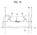
- FIGs. 10 and 11 are circuit diagrams showing the structure of the nonvolatile semiconductor memory device according to the present embodiment.
- the memory cell 10 of the nonvolatile semiconductor memory device includes, as shown in FIG. 10 , a resistance memory element 12, a cell select transistor 14, and a current control transistor 18 as a variable resistor.
- the resistance memory element 12 has one end connected to the drain terminal of the cell select transistor 14 and the other end connected to the source terminal of the current control transistor 18.
- the cell select transistor 14 has the source terminal connected to a source line SL and the gate terminal connected to a word line WL.
- the current control transistor has the drain terminal connected to a bit line BL and the gate terminal connected to a control line CL.
- the resistance memory element 12 has a resistance memory material sandwiched between a pair of electrodes.
- the resistance memory material may be a unipolar resistance memory material or a unipolar resistance memory material.
- the resistance memory material is, e.g., a unipolar resistance material of, e.g., TiO x .
- FIG. 11 is a circuit diagram of the memory cell array of the memory cells 10 arranged in a matrix.
- a plurality of memory cells 10 is formed adjacent to each other in the column direction (vertically in the drawing) and the row direction (horizontally in the drawing).
- a plurality of word lines WL1, /WL1, WL2, /WL2 ..., control lines CL1, /CL1, CL2, /CL2 ..., and source lines SL1, SL2 ... are arranged, forming signal lines common among the memory cells 10 arranged in the column direction.
- the source lines SL are provided each for two word lines WL.
- bit lines BL1, BL2, BL3, BL4 ... are arranged, forming signal lines common among the memory cells 10 arranged row direction.
- the voltage of the control lines CL in the present embodiment corresponds to the gate voltage of the bit line select transistor in FIGs. 7 and 8 .
- the memory cell 10 to be rewritten is a memory cell 10 connected to the word line WL1 and the bit line BL1.
- a prescribed voltage is applied to the control line CL1 to turn on the current control transistor 16 (refer to FIG. 7 ).
- the voltage to be applied to the control line CL1 is controlled so that the channel resistance R CL of the current control transistor 18 is sufficiently smaller than the resistance value R H of the resistance memory element 12 in the high resistance state and has a value which cannot be ignored in comparison with the resistance value R L of the resistance memory element 12 in the low resistance state.
- a prescribed voltage is applied to the word line WL1 to turn on the cell select transistor 14 (refer to FIG. 7 ).
- the voltage to be applied to the word line WL1 is controlled so that the channel resistance R CS of the cell select transistor 14 has a value which is ignorably small in comparison with the resistance value R L of the resistance memory element 12 in the low resistance state.
- the source line SL1 is connected to a reference potential, e.g., 0 V, which is the ground potential (refer to FIG. 7 ).
- a bias voltage which is the same as the voltage necessary to set the resistance memory element 12 or a little larger than the voltage is applied (refer to FIG. 7 ).
- a current passage to the source line SL1 via the bit line BL1, the current control transistor 18, the resistance memory element 12 and the cell select transistor 14 is formed, and the applied bias voltage is divided to the resistance memory element 12, the current control transistor 16 and the cell select transistor 14, corresponding to the resistance value R H of the resistance memory element 12, the channel resistance R CL of the current control transistor 16 and the channel resistance R CS of the cell select transistor 14.
- the resistance value R H of the resistance memory element 12 is sufficiently large in comparison with the channel resistance R CL of the current control transistor 18 and the channel resistance R CS of the cell select transistor, and most the bias voltage is applied to the resistance memory element 12.
- the resistance memory element 12 changes from the high resistance state to the low resistance state.
- the channel resistance R CL of the current control transistor 18 can be set at an arbitrary value as far as the performance of the current control transistor 18 permits, and the voltage to be applied to the resistance memory element 12, i.e., the current to flow in the resistance memory element 12 can be set at an arbitrary value by the gate voltage of the current control transistor 18, i.e., the applied voltage to the control line CL1.
- the current to flow in the resistance memory element 12 can be limited to a prescribed value, and by this current limitation, the resistance value of the resistance memory element 12 can controlled.
- the value of the current to flow in the resistance memory element 12 is limited to not more than 10 mA, whereby the resistance memory element 12 has the resistance characteristics indicated by the curve "a”, and the value of the current to flow in the resistance memory element 12 is limited to not more than 15 mA, whereby the resistance memory element 12 has the resistance characteristics indicated by the curve "b”, and the value of the current flowing in the resistance memory element 12 is limited to not more than 20 mA, whereby the resistance memory element 12 has the resistance characteristics indicated by the curve "c".
- the memory cell 10 to be rewritten is a memory cell 10 connected to the word line WL1 and the bit line BL1.
- a prescribed voltage is applied to the control line CL1 to turn on the current control transistor 18 (refer to FIG. 8 ).
- the voltage to be applied to the control line CL1 is controlled so that the channel resistance R CL of the current control transistor 18 is sufficiently smaller than the resistance value R L of the resistance memory element 12 in the low resistance state.
- a prescribed voltage is applied to the word line WL1 to turn on the cell select transistor 14 (refer to FIG. 8 ).
- the voltage to be applied to the word line WL1 is controlled so that the channel resistance R CS of the cell select transistor 14 is sufficiently smaller than the resistance value R L of the resistance memory element 12 in the low resistance state.
- the source line SL1 is connected to a reference potential, e.g., 0 V, which is the ground potential (refer to FIG. 8 ).
- a bias voltage which is the same as or a little larger than the voltage necessary to reset the resistance memory element 12 is applied (refer to FIG. 8 ).
- a current passage to the source line SL1 via the bit line BL1 the current control transistor 18, the resistance memory element 12 and the cell select transistor 14 is formed, and the applied bias voltage is divided to the resistance memory element 12, the current control transistor 18 and the cell select transistor 14, corresponding to the resistance value R L of the resistance memory element 12, the channel resistance R CL of the current control transistor 18 and the channel resistance R CS of the cell select transistor 14.
- the channel resistance R CL of the current control transistor 18 and the channel resistance R CS of the cell select transistor 14 are sufficiently smaller than the resistance value R L of the resistance memory element 12, and most of the applied bias voltage is applied to the resistance memory element 12.
- the resistance memory element 12 changes from the low resistance state to the high resistance state.
- the bias voltage to be applied to the bit line BL must be smaller than the voltage necessary for the setting.
- the gate voltages of these transistors are adjusted so that the channel resistance R CL of the current control transistor 18 and the channel resistance R CS of the cell select transistor 14 are sufficiently smaller than the resistance value R L of the resistance memory element 12 while the bias voltage to be applied to the bit line BL is set to be not less than the voltage necessary for the resetting and less than the voltage necessary for the setting.
- the word lines WL and the source lines SL are arranged in column direction, and the memory cells 10 connected to one word line (e.g., WL1) are connected to the same source line SL (e.g., SL1).
- a plurality of bit lines BL e.g., BL1 - BL4 are simultaneously driven, whereby a plurality of memory cells 10 connected to a select word line (e.g., WL1) can be reset at once.
- the memory cell to be read is a memory cell 10 connected to the word line WL1 and the bit line BL1.
- a prescribed voltage is applied to the control line CL1 to turn on the current control transistor 18 (refer to FIG. 9 ).
- the voltage to be applied to the control line CL1 is controlled so that the channel resistance R CL of the current control transistor 18 is sufficiently smaller than the resistance value R L of the resistance memory element 12.
- a prescribed voltage is applied to the word line WL1 to turn on the cell select transistor 14 (refer to FIG. 9 ).
- the voltage to be applied to the word line WL1 is controlled so that the channel resistance R cs of the cell select transistor 14 is sufficiently smaller than the resistance value R L of the resistance memory element 12 in the low resistance state.
- the source line SL1 is connected to a reference potential, e.g., 0 V, which is the ground potential (refer to FIG. 9 ).
- a prescribed bias voltage is applied to the bit line BL1 (refer to FIG. 9 ).
- This bias voltage is set in accordance with the memory characteristics given by the lowest current limitation value. That is, the value of the bias voltage is set so that even with the resistance memory element 12 having any resistance state, neither the setting nor the resetting is caused by the applied voltage.
- the bias voltage for reading is set at a voltage of less than 0.6 V (e.g., 0.5 V) which sufficiently ensures a margin.
- the resistor when the resistance memory element is switched from the high resistance state to the low resistance state, the resistor is serially connected to the resistance memory element to thereby prevent the flow of large current to the resistance memory element, whereby the breakage and degradation of the resistance memory element due to the flow of the large current can be prevented.
- the resistance value of the resistor By the resistance value of the resistor, the resistance value of the resistance memory element in the low resistance state can be controlled.
- the multiple-valued memory can be easily realized.
- the nonvolatile semiconductor memory device and the method of writing into the same according to a fourth embodiment of the present invention will be explained.
- the same members of the present embodiment as those of the nonvolatile semiconductor memory device, the method of writing into the same and the method of reading the same according to the third embodiment shown in FIGs. 10 and 11 are represented by the same reference numbers not to repeat or to simplify their explanation.
- the nonvolatile semiconductor memory device according to the present embodiment is the same as the nonvolatile semiconductor memory device according to the third embodiment shown in FIGS. 10 and 11 except that in the former, the resistance memory element 12 is formed of a bipolar resistance memory material.
- the bipolar resistance memory material can be, e.g., Cr-doped SrZrO 3 or others.
- a negative bias voltage is applied for the setting, and for the resetting, a positive bias voltage is applied.
- the method of writing into the nonvolatile semiconductor memory device according to the present embodiment is the same as the method of writing into the nonvolatile semiconductor memory device according to the third embodiment except the polarity of the bias voltage.
- the memory cell 10 to be rewritten is a memory cell 10 connected to the word line WL1 and to the bit line BL1.
- a prescribed voltage is applied to the control line CL1 to turn on the current control transistor 18.
- the voltage to be applied to the control line CL1 is controlled so that the channel resistance R CL of the current control transistor 18 is sufficiently smaller than the resistance value R H of the resistance memory element 12 in the high resistance state and has a value which is cannot be ignored in comparison with the resistance value R L of the resistance memory element 12 in the low resistance state.
- a prescribed voltage is applied to the word line WL1 to turn on the cell select transistor 14.
- the voltage to be applied to the word line WL1 is controlled so that the channel resistance R CS of the cell select transistor 14 has a value which is ignorably small in comparison with the resistance value R L of the resistance memory element 12 in the low resistance state.
- the source line SL1 is connected to a reference potential, e.g., 0 V, which is the ground potential.
- a negative bias voltage which is the same as the voltage necessary to setting the resistance memory element 12 or has an absolute value a little larger than the voltage is applied.
- the applied voltage is divided to the resistance memory element 12, the current control transistor 18 and the cell select transistor 14, corresponding to the resistance value R H of the resistance memory element 12, the channel resistance R CL of the current control transistor 18 and the channel resistance R CS of the cell select transistor 14.
- the resistance value R H of the resistance memory element 12 is sufficiently large in comparison with the channel resistance R CL of the current control transistor 18 and the channel resistance R CS of the cell select transistor 14, and most of the bias voltage is applied to the resistance memory element 12.
- the resistance memory element 12 changes from the high resistance state to the low resistance state.
- the channel resistance R CL of the current control transistor 18 can be set at an arbitrary value as far as the performance of the current control transistor 18 permits, and the voltage to be applied to the resistance memory element 12, i.e., current to flow in the resistance memory element 12 can be set at an arbitrary value by the gate voltage of the current control transistor 18, i.e., the applied voltage to the control line CL1.
- the current to flow in the resistance memory element 12 can be limited to a prescribed value. By this current limitation, the resistance value of the resistance memory element 12 can be controlled.
- the memory cell 10 to be rewritten is a memory cell 10 connected to the word line WL1 and the bit line BL1.
- a prescribed voltage is applied to the control line CL1 to turn on the current control transistor 18.
- the voltage to be applied to the control line CL1 is controlled so that the channel resistance R CL of the current control transistor 18 becomes sufficiently smaller than the resistance value R L of the resistance memory element 12 in the low resistance state.
- a prescribed voltage is applied to the word line WL1 to turn on the cell select transistor 14.
- the voltage to be applied to the word line WL1 is controlled so that the channel resistance R CS of the cell select transistor 14 becomes sufficiently smaller than the resistance value R L of the resistance memory element 12 in the low resistance state.
- the source line SL1 is connected to a reference potential, e.g., 0 V, which is the ground potential.
- a positive bias voltage which is the same as or has an absolute value larger than the voltage necessary to reset the resistance memory element 12 is applied.
- a current passage from the source line SL1 via the cell select transistor 14, the resistance memory element 12, the current control transistor 18 and the bit line BL1 is formed, and the applied bias voltage is divided to the resistance memory element 12, the current control transistor 18 and the cell select transistor 14, corresponding to the resistance value R L of the resistance memory element 12, the channel resistance R CL of the current control transistor 18 and the channel resistance R CS of the cell select transistor 14.
- the channel resistance R BS of the current control transistor 18 and channel resistance R CS of the cell select transistor 14 are sufficiently smaller than the resistance value R L of the resistance memory element 12, which permits almost all the applied bias voltage is applied to the resistance memory element 12.
- the resistance memory element 12 changes from the low resistance state to the high resistance state.
- the word lines WL and the source lines SL are arranged in column direction, and the memory cells 10 connected to one word line (e.g., WL1) are connected to the same source line SL (e.g., SL1).
- a plurality of bit lines BL e.g., BL1 - BL4 are simultaneously driven, whereby a plurality of memory cells 10 connected to a select word line (e.g., WL1) can be reset at once.
- the memory cell 10 to be read is a memory cell 10 connected to the word line WL1 and the bit line BL1.
- a prescribed voltage is applied to the control line CL1 to turn on the current control transistor 18.
- the voltage to be applied to the control line CL1 is controlled so that the channel resistance R CL of the current control transistor 18 is sufficiently smaller than the resistance value R L of the resistance memory element 12.
- a prescribed voltage is applied to the word line WL1 to turn on the cell select transistor 14.
- the voltage to be applied to the word line WL is controlled so that the channel resistance R cs of the cell select transistor 14 becomes sufficiently smaller than the resistance value R L of the resistance memory element 12 in the low resistance state.
- the source line SL1 is connected to a reference potential, e.g., 0 V, which is the ground potential.
- bias voltage is set in accordance with the memory characteristics given by the lowest current limitation value. That is, the value of the bias voltage is set so that even with the resistance memory element 12 in any resistance state, neither the setting nor the resetting is caused by the applied voltage.
- the resistor when the resistance memory element is switched from the high resistance state to the low resistance state, the resistor is serially connected to the resistance memory element to thereby prevent the flow of large current to the resistance memory element, whereby the breakage and degradation of the resistance memory element due to the flow of the large current can be prevented.
- the resistance value of the resistor By the resistance value of the resistor, the resistance value of the resistance memory element in the low resistance state can be controlled.
- the multiple-valued memory can be easily realized.
- the nonvolatile semiconductor memory device and the method of writing into the same according to a fifth embodiment of the present invention will be explained with reference to FIG. 12 .
- the same members of the present embodiment as those of the nonvolatile semiconductor memory device, the method of writing into the same and the method of reading the same according to first to the fourth embodiments shown in FIGs. 1 to 11 are represented by the same reference numbers not to repeat or to simplify their explanation.
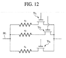
- FiG. 12 is a circuit diagram showing the structure of the nonvolatile semiconductor memory device according to the present embodiment.
- the channel resistance R BS of the bit line select transistor 16 is controlled to thereby control the current to flow in the bit line BL, but the method for controlling the current to flow in the bit line BL is not limited to this.
- the variable resistance circuit shown in FIG. 12 can be provided in place of the bit line select transistor 16 shown in FIG. 6 .
- the circuit shown in FIG. 12 is formed by parallelly connecting a plurality of series connection of the resistor r and the select transistor Tr.
- the resistance value of the resistor r 1 , r 2 , ..., r n are set suitably corresponding to the write/read characteristics of the nonvolatile semiconductor memory device.
- At least one of the select transistors Tr 1 , Tr 2 , ... , or Tr n is turned on, whereby the resistor r 1 , r 2 , ... , or r n are serially connected to the bit line BL. Accordingly, by the resistance value of the resistor r 1 , r 2 , ..., r n , the limitation value of the current to flow in the resistance memory element 12 in the setting can be suitably controlled. This current limitation value can be changed only by switching the select transistors Tr 1 , Tr 2 , ..., Tr n to be turned on, which makes the control easy in comparison with controlling the channel resistance R BS of the bit line select transistor 16.
- the resistor having a sufficiently smaller resistance value than the resistance value R L of the resistance memory element in the low resistance state (e.g., r n ) may be connected, which also makes the control easy in comparison with controlling the channel resistance R BS of the bit line select transistor 16.
- Two or more of the select transistors Tr may be turned on at once.
- the resistance value with the select transistor Tr 1 turned on is r 1
- the resistance value with the select transistor Tr 2 turned on is r 2
- the resistance value with the select transistors Tr 1 , Tr 2 simultaneously turned on is r 1 r 2 /(r 1 +r 2 ). Accordingly, by suitably combining the select transistors Tr to be turned on, more resistance states can be realized, which allows the circuit structure to be simplified.
- the resistance value of the resistor serially connected to the resistance memory elements can be easily controlled.
- a multiple-valued memory can be realized.
- the nonvolatile semiconductor memory device and the method of manufacturing the same according to a sixth embodiment of the present invention will be explained with reference to FIGs 13 to 16 .
- FIG. 13 is a plan view showing the structure of the nonvolatile semiconductor memory device according to the present embodiment.
- FIG. 14 is a diagrammatic sectional view showing the structure of the nonvolatile semiconductor memory device according to the present embodiment.
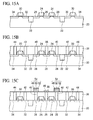
- FIGs. 15 and 16 are sectional views showing the method of manufacturing the nonvolatile semiconductor memory device according to the present embodiment.
- a device isolation film 22 for defining device regions is formed in a silicon substrate 10.
- cell select transistors each including a gate electrode 24 and source/drain regions 26, 28 and current control transistors each including a gate electrode 30 and source/drain regions 32, 34 are formed.
- the gate electrodes 24 function also as word lines WL commonly connecting the gate electrodes 24 of the cell select transistors adjacent in the column direction (vertically in the drawing), and the gate electrodes 30 function also as control lines CL commonly connecting the gate electrodes 30 of the current control transistors adjacent in the column direction.
- an inter-layer insulating film 36 with contact plugs 38 electrically connected to the source/drain regions 26, contact plugs 40 electrically connected to the source/drain regions 28, contact plugs 42 electrically connected to the source/drain regions 32 and contact plugs 44 electrically connected to the source/drain regions 34 buried in is formed.
- the source lines 46 electrically connected to the source/drain regions 28 via the contact plugs 38, and resistance memory elements 54 electrically connected to the source/drain regions 30 via the contact plugs 40 are formed.
- an inter-layer insulating film 56 with contact plugs 58 electrically connected to the resistance memory elements 54 and contact plugs 60 electrically connected to the contact plugs 42 buried in is formed.
- an interconnection layer 62 connecting between the contact plugs 58, 60 is formed.
- an inter-layer insulating film 64 is formed over the inter-layer insulating film 56 with the interconnection layer 62 formed on.
- bit lines 68 electrically connected to the source drain regions 34 via the contact plugs 66 buried in the inter-layer insulating films 64, 56 and the contact plugs 44 are formed.
- the nonvolatile semiconductor memory device according to the third embodiment shown in FIG. 11 is constituted.
- the device isolation film 22 for defining the device regions is formed by, e.g., STI (Shallow Trench Isolation) method.
- the cell select transistors each including the gate electrode 24 and the source/drain regions 26, 28 and the current control transistors each including the gate electrode 30 and the source/drain regions 32, 34 are formed in the same way as in the usual MOS transistor manufacturing method ( FIG. 15A ).
- a silicon oxide film is deposited by, e.g., CVD method to form the inter-layer insulating film 36 of the silicon oxide film.
- the contact holes reaching down to the source/drain regions 26, 28, 32, 34 are formed in the inter-layer insulating film 36.
- a barrier metal and a tungsten film are deposited, and then these conductive films are etched back to form the contact plugs 38, 40, 42, 44 electrically connected to the source/drain regions 26, 28, 32, 34 in the inter-layer insulating film 36 ( FIG. 15B ).
- the source lines 46 electrically connected to the source/drain regions 26 via the contact plugs 38 and the resistance memory elements 54 electrically connected to the source/drain regions 28 via the contact plugs 40 are formed ( FIG. 15C ).
- the resistance memory elements 54 each includes a lower electrode 40 connected to the contact plug 40, a resistance memory material layer 50 formed on the lower electrode 48 and an upper electrode 52 formed on the resistance memory material layer 50.
- the resistance memory material layer 46 is formed of the bipolar resistance memory material, for example, Pr 1-x Ca x MnO 3 (x ⁇ 1), La 1-x Ca x MnO 3 (x ⁇ 1), SrTiO 3 doped with Cr, Nb or others, SrZrO 3 doped with Cr, Nb or others or others is formed by laser ablation, sol-gel method, sputtering method, MOCVD method or others.
- the resistance memory material layer 46 is formed of the unipolar resistance memory material, for example, a film of NiO y (y ⁇ 1), TiO z (z ⁇ 2), HfO z (z ⁇ 2) or others is formed by sol-gel method, sputtering method, MOCVD method or others.
- a silicon oxide film is deposited by, e.g., CVD method to form the inter-layer insulating film 56 of the silicon oxide film.
- a barrier metal and a tungsten film are deposited by, e.g., CVD method, and then these conductive films are etched back to form the contact plugs 58 electrically connected to the upper electrodes 52 of the resistance memory elements 54 and the contact plugs 60 electrically connected to the contact plugs 42 in the inter-layer insulating film 56 ( FIG. 16A ).
- a conductive film is deposited, and then the conductive film is patterned by photolithography and dry etching to form the interconnection layer 62 electrically connected to the contact plugs 58 and the contact plugs 60 ( FIG. 16B ).
- a silicon oxide film is deposited by, e.g., CVD method to form the inter-layer insulating film 64 of the silicon oxide film.
- contact holes reaching down to the contact plugs 44 are formed in the inter-layer insulating films 64, 56.
- a barrier metal and a tungsten film are deposited, and then these conductive films are etched back to form the contact plugs 66 electrically connected to the contact plugs 44 in the inter-layer insulating films 64, 56.
- bit lines 68 electrically connected to the source/drain regions 34 via the contact plugs 66, 44 ( FIG. 16C ).
- TiO x is used as the unipolar resistance memory material, and as the bipolar resistance memory material, Cr-doped SrZrO 3 is used.
- the material forming the resistance memory element is not limited to them.
- the unipolar resistance memory material NiO x , etc. can be used, and as the bipolar resistance memory material, Pr 1-x Ca x MnO 3 or La 1-x Ca x MnO 3 exhibiting CMR (Colossal Magneto-Resistance), etc. can be used.
- the applied voltage and the current limitation value for the setting and the resetting are set suitably depending on kinds of the resistance memory material, structures of the resistance memory elements, etc.
- the source lines SL are arranged in parallel with the word lines WL but may be arranged in parallel with the bit lines BL.
- the source lines SL1, SL2 ... may be extended in row direction between the memory cells adjacent in column direction.
- the source lines SL1, SL2 ... may be extended in row direction between the memory cells adjacent in column direction.
- one memory cell comprises one cell select transistor and one resistance memory element but may not have essentially this constitution.
- one memory cell may comprise one cell select transistor and two resistance memory elements or two cell select transistors and two resistance memory elements.
- the nonvolatile semiconductor memory device and the method of writing into the same according to the present invention can prevent the degradation of the elements when the resistance state is switched and can realize two or more resistance states with good reproducibility.
- the nonvolatile semiconductor memory device and the method of writing into the same according to the present invention are very useful to improve the reliability and memory capacity of the nonvolatile semiconductor memory devices.
Landscapes
- Engineering & Computer Science (AREA)
- Chemical & Material Sciences (AREA)
- Materials Engineering (AREA)
- Computer Hardware Design (AREA)
- Semiconductor Memories (AREA)
- Read Only Memory (AREA)
Applications Claiming Priority (1)
| Application Number | Priority Date | Filing Date | Title |
|---|---|---|---|
| PCT/JP2005/011249 WO2006137111A1 (fr) | 2005-06-20 | 2005-06-20 | Memoire a semi-conducteurs non volatile et procede d'ecriture pour une telle memoire |
Publications (2)
| Publication Number | Publication Date |
|---|---|
| EP1895540A1 true EP1895540A1 (fr) | 2008-03-05 |
| EP1895540A4 EP1895540A4 (fr) | 2008-07-09 |
Family
ID=37570164
Family Applications (1)
| Application Number | Title | Priority Date | Filing Date |
|---|---|---|---|
| EP05750964A Withdrawn EP1895540A4 (fr) | 2005-06-20 | 2005-06-20 | Memoire a semi-conducteurs non volatile et procede d'ecriture pour une telle memoire |
Country Status (4)
| Country | Link |
|---|---|
| US (1) | US20080123393A1 (fr) |
| EP (1) | EP1895540A4 (fr) |
| JP (1) | JPWO2006137111A1 (fr) |
| WO (1) | WO2006137111A1 (fr) |
Cited By (1)
| Publication number | Priority date | Publication date | Assignee | Title |
|---|---|---|---|---|
| WO2010080334A1 (fr) * | 2008-12-19 | 2010-07-15 | Sandisk 3D Llc | Programmation d'une cellule de mémoire au moyen d'une diode en série par application d'une polarisation inverse |
Families Citing this family (34)
| Publication number | Priority date | Publication date | Assignee | Title |
|---|---|---|---|---|
| JP4203506B2 (ja) * | 2006-01-13 | 2009-01-07 | シャープ株式会社 | 不揮発性半導体記憶装置及びその書き換え方法 |
| WO2007145295A1 (fr) * | 2006-06-16 | 2007-12-21 | Panasonic Corporation | Dispositif mémoire non volatile |
| US7920402B2 (en) | 2006-11-17 | 2011-04-05 | Panasonic Corporation | Resistance variable memory apparatus |
| JP4221031B2 (ja) * | 2007-02-09 | 2009-02-12 | シャープ株式会社 | 不揮発性半導体記憶装置及びその書き換え方法 |
| WO2008105155A1 (fr) * | 2007-02-23 | 2008-09-04 | Panasonic Corporation | Périphérique de mémoire non volatile et procédé pour écrire des données dans un périphérique de mémoire non volatile |
| US8094481B2 (en) | 2007-03-13 | 2012-01-10 | Panasonic Corporation | Resistance variable memory apparatus |
| JP4157582B1 (ja) * | 2007-03-26 | 2008-10-01 | シャープ株式会社 | 半導体記憶装置 |
| JP2009037703A (ja) * | 2007-08-02 | 2009-02-19 | Toshiba Corp | 抵抗変化メモリ |
| CN101802921B (zh) | 2007-09-10 | 2013-08-28 | 松下电器产业株式会社 | 非易失性存储装置和向非易失性存储装置的数据写入方法 |
| JP5159224B2 (ja) | 2007-09-21 | 2013-03-06 | 株式会社東芝 | 抵抗変化メモリ装置 |
| JP5121439B2 (ja) | 2007-12-26 | 2013-01-16 | 株式会社東芝 | 不揮発性半導体記憶装置 |
| US8094485B2 (en) * | 2008-05-22 | 2012-01-10 | Panasonic Corporation | Variable resistance nonvolatile storage device with oxygen-deficient oxide layer and asymmetric substrate bias effect |
| US8270199B2 (en) * | 2009-04-03 | 2012-09-18 | Sandisk 3D Llc | Cross point non-volatile memory cell |
| US8139391B2 (en) | 2009-04-03 | 2012-03-20 | Sandisk 3D Llc | Multi-bit resistance-switching memory cell |
| US7978498B2 (en) * | 2009-04-03 | 2011-07-12 | Sandisk 3D, Llc | Programming non-volatile storage element using current from other element |
| CN102077297A (zh) | 2009-05-14 | 2011-05-25 | 松下电器产业株式会社 | 非易失性存储装置和向非易失性存储装置写入数据的方法 |
| KR20110015256A (ko) | 2009-08-07 | 2011-02-15 | 삼성전자주식회사 | 가변 저항 메모리 장치 및 그것의 프로그램 방법 |
| JP5462027B2 (ja) * | 2010-02-22 | 2014-04-02 | 株式会社東芝 | 不揮発性半導体記憶装置 |
| US8441839B2 (en) | 2010-06-03 | 2013-05-14 | Panasonic Corporation | Cross point variable resistance nonvolatile memory device |
| JP5527729B2 (ja) | 2010-08-26 | 2014-06-25 | 独立行政法人産業技術総合研究所 | メモリ素子の駆動方法及びメモリ素子を備える記憶装置 |
| JP5499364B2 (ja) | 2010-08-26 | 2014-05-21 | 独立行政法人産業技術総合研究所 | メモリ素子の駆動方法及びメモリ素子を備える記憶装置 |
| WO2012098897A1 (fr) * | 2011-01-20 | 2012-07-26 | パナソニック株式会社 | Circuit de verrouillage non volatil et circuit eccles-jordan non volatil |
| WO2012108185A1 (fr) | 2011-02-10 | 2012-08-16 | パナソニック株式会社 | Procédé d'attaque et procédé d'initialisation d'un élément de stockage non volatile, ainsi que dispositif de stockage non volatile |
| JP2012204399A (ja) * | 2011-03-23 | 2012-10-22 | Toshiba Corp | 抵抗変化メモリ |
| US9305644B2 (en) | 2011-06-24 | 2016-04-05 | Rambus Inc. | Resistance memory cell |
| JP5226158B1 (ja) | 2011-11-22 | 2013-07-03 | パナソニック株式会社 | 不揮発性ラッチ回路、不揮発性フリップフロップ回路および不揮発性信号処理装置 |
| US8885387B2 (en) | 2011-12-02 | 2014-11-11 | Panasonic Corporation | Cross point variable resistance nonvolatile memory device |
| WO2013157261A1 (fr) | 2012-04-20 | 2013-10-24 | パナソニック株式会社 | Procédé de commande d'un élément de mémoire rémanente, et dispositif de mémoire rémanente |
| US8861255B2 (en) | 2012-05-15 | 2014-10-14 | Micron Technology, Inc. | Apparatuses including current compliance circuits and methods |
| US9437291B2 (en) | 2014-02-26 | 2016-09-06 | Rambus Inc. | Distributed cascode current source for RRAM set current limitation |
| US9286976B2 (en) * | 2014-05-29 | 2016-03-15 | Intel Corporation | Apparatuses and methods for detecting write completion for resistive memory |
| US9336881B2 (en) * | 2014-06-16 | 2016-05-10 | Panasonic Intellectual Property Management Co., Ltd. | Variable resistance nonvolatile memory device including a variable resistance layer that changes reversibly between a low resistance state and a high resistance state according to an applied electrical signal |
| US12548620B2 (en) * | 2024-05-08 | 2026-02-10 | Taiwan Semiconductor Manufacturing Company, Ltd. | Memory device and operating method thereof |
| US20260088084A1 (en) * | 2024-09-25 | 2026-03-26 | Intel Corporation | Compute-in-memory arrays |
Family Cites Families (9)
| Publication number | Priority date | Publication date | Assignee | Title |
|---|---|---|---|---|
| US6473332B1 (en) | 2001-04-04 | 2002-10-29 | The University Of Houston System | Electrically variable multi-state resistance computing |
| WO2002091385A1 (fr) * | 2001-05-07 | 2002-11-14 | Advanced Micro Devices, Inc. | Cellule de memoire moleculaire |
| JP2004185755A (ja) * | 2002-12-05 | 2004-07-02 | Sharp Corp | 不揮発性半導体記憶装置 |
| JP4113493B2 (ja) | 2003-06-12 | 2008-07-09 | シャープ株式会社 | 不揮発性半導体記憶装置及びその制御方法 |
| JP4567963B2 (ja) | 2003-12-05 | 2010-10-27 | ルネサスエレクトロニクス株式会社 | 半導体集積回路装置 |
| JP4670252B2 (ja) * | 2004-01-20 | 2011-04-13 | ソニー株式会社 | 記憶装置 |
| JP4475174B2 (ja) * | 2005-06-09 | 2010-06-09 | ソニー株式会社 | 記憶装置 |
| US7362604B2 (en) * | 2005-07-11 | 2008-04-22 | Sandisk 3D Llc | Apparatus and method for programming an array of nonvolatile memory cells including switchable resistor memory elements |
| JP2007080311A (ja) * | 2005-09-12 | 2007-03-29 | Sony Corp | 記憶装置及び半導体装置 |
-
2005
- 2005-06-20 JP JP2007522135A patent/JPWO2006137111A1/ja not_active Withdrawn
- 2005-06-20 WO PCT/JP2005/011249 patent/WO2006137111A1/fr not_active Ceased
- 2005-06-20 EP EP05750964A patent/EP1895540A4/fr not_active Withdrawn
-
2007
- 2007-12-19 US US11/959,781 patent/US20080123393A1/en not_active Abandoned
Cited By (2)
| Publication number | Priority date | Publication date | Assignee | Title |
|---|---|---|---|---|
| WO2010080334A1 (fr) * | 2008-12-19 | 2010-07-15 | Sandisk 3D Llc | Programmation d'une cellule de mémoire au moyen d'une diode en série par application d'une polarisation inverse |
| US7944728B2 (en) | 2008-12-19 | 2011-05-17 | Sandisk 3D Llc | Programming a memory cell with a diode in series by applying reverse bias |
Also Published As
| Publication number | Publication date |
|---|---|
| WO2006137111A1 (fr) | 2006-12-28 |
| JPWO2006137111A1 (ja) | 2009-01-08 |
| EP1895540A4 (fr) | 2008-07-09 |
| US20080123393A1 (en) | 2008-05-29 |
Similar Documents
| Publication | Publication Date | Title |
|---|---|---|
| EP1895540A1 (fr) | Memoire a semi-conducteurs non volatile et procede d'ecriture pour une telle memoire | |
| US7532497B2 (en) | Nonvolatile semiconductor memory device and method of writing into the same | |
| US7643328B2 (en) | Method of writing into semiconductor memory device | |
| US7898839B2 (en) | Semiconductor memory device and method of writing into semiconductor memory device | |
| US7668002B2 (en) | Resistance memory element and nonvolatile semiconductor memory | |
| KR101002612B1 (ko) | 불휘발성 반도체 기억 장치 및 그 기입 방법, 판독 방법 및 소거 방법 | |
| US8411484B2 (en) | Semiconductor memory device and method of writing into the same | |
| US9792985B2 (en) | Resistive volatile/non-volatile floating electrode logic/memory cell | |
| JP5551769B2 (ja) | メモリ素子、積層体、メモリマトリックス及びそれらの動作方法 | |
| US20080170428A1 (en) | Nonvolatile semiconductor memory device and method of writing into the same | |
| EP1914806A1 (fr) | Element de resistance variable et procede de fabrication idoine et dispositif de stockage pourvu dudit element | |
| US20080232154A1 (en) | Resistance memory element and method of manufacturing the same, and semiconductor memory device | |
| KR20050085533A (ko) | 메모리 및 액세스 디바이스 | |
| KR20030003025A (ko) | 전기적으로 프로그램가능한 저 누화 저항 교점 메모리 | |
| JP2008065953A (ja) | 不揮発性半導体記憶装置及びその読み出し方法 | |
| JP2014063549A (ja) | 半導体記憶装置 | |
| KR20080009315A (ko) | 불휘발성 반도체 기억 장치 및 그 기입 방법 | |
| KR20080040734A (ko) | 불휘발성 반도체 기억 장치 및 그 기입 방법 |
Legal Events
| Date | Code | Title | Description |
|---|---|---|---|
| PUAI | Public reference made under article 153(3) epc to a published international application that has entered the european phase |
Free format text: ORIGINAL CODE: 0009012 |
|
| 17P | Request for examination filed |
Effective date: 20080116 |
|
| AK | Designated contracting states |
Kind code of ref document: A1 Designated state(s): DE FR GB |
|
| A4 | Supplementary search report drawn up and despatched |
Effective date: 20080610 |
|
| DAX | Request for extension of the european patent (deleted) | ||
| RBV | Designated contracting states (corrected) |
Designated state(s): DE FR GB |
|
| 17Q | First examination report despatched |
Effective date: 20080929 |
|
| STAA | Information on the status of an ep patent application or granted ep patent |
Free format text: STATUS: THE APPLICATION IS DEEMED TO BE WITHDRAWN |
|
| 18D | Application deemed to be withdrawn |
Effective date: 20090708 |