EP1895542A2 - Dispositif de mémoire flash doté de fonctionnalités de réintroductions multi-page et procédés de remplacement de blocs correspondants - Google Patents
Dispositif de mémoire flash doté de fonctionnalités de réintroductions multi-page et procédés de remplacement de blocs correspondants Download PDFInfo
- Publication number
- EP1895542A2 EP1895542A2 EP07016257A EP07016257A EP1895542A2 EP 1895542 A2 EP1895542 A2 EP 1895542A2 EP 07016257 A EP07016257 A EP 07016257A EP 07016257 A EP07016257 A EP 07016257A EP 1895542 A2 EP1895542 A2 EP 1895542A2
- Authority
- EP
- European Patent Office
- Prior art keywords
- page
- address
- memory
- program
- memory device
- Prior art date
- Legal status (The legal status is an assumption and is not a legal conclusion. Google has not performed a legal analysis and makes no representation as to the accuracy of the status listed.)
- Withdrawn
Links
Images


Classifications
-
- G—PHYSICS
- G06—COMPUTING OR CALCULATING; COUNTING
- G06F—ELECTRIC DIGITAL DATA PROCESSING
- G06F12/00—Accessing, addressing or allocating within memory systems or architectures
- G06F12/02—Addressing or allocation; Relocation
-
- G—PHYSICS
- G11—INFORMATION STORAGE
- G11C—STATIC STORES
- G11C16/00—Erasable programmable read-only memories
- G11C16/02—Erasable programmable read-only memories electrically programmable
- G11C16/06—Auxiliary circuits, e.g. for writing into memory
- G11C16/10—Programming or data input circuits
- G11C16/102—External programming circuits, e.g. EPROM programmers; In-circuit programming or reprogramming; EPROM emulators
-
- G—PHYSICS
- G06—COMPUTING OR CALCULATING; COUNTING
- G06F—ELECTRIC DIGITAL DATA PROCESSING
- G06F12/00—Accessing, addressing or allocating within memory systems or architectures
-
- G—PHYSICS
- G11—INFORMATION STORAGE
- G11C—STATIC STORES
- G11C11/00—Digital stores characterised by the use of particular electric or magnetic storage elements; Storage elements therefor
- G11C11/56—Digital stores characterised by the use of particular electric or magnetic storage elements; Storage elements therefor using storage elements with more than two stable states represented by steps, e.g. of voltage, current, phase, frequency
- G11C11/5621—Digital stores characterised by the use of particular electric or magnetic storage elements; Storage elements therefor using storage elements with more than two stable states represented by steps, e.g. of voltage, current, phase, frequency using charge storage in a floating gate
- G11C11/5628—Programming or writing circuits; Data input circuits
-
- G—PHYSICS
- G11—INFORMATION STORAGE
- G11C—STATIC STORES
- G11C16/00—Erasable programmable read-only memories
- G11C16/02—Erasable programmable read-only memories electrically programmable
- G11C16/06—Auxiliary circuits, e.g. for writing into memory
- G11C16/34—Determination of programming status, e.g. threshold voltage, overprogramming or underprogramming, retention
- G11C16/3418—Disturbance prevention or evaluation; Refreshing of disturbed memory data
Definitions
- the present invention relates to a method of executing a multi-page copyback program in a non-volatile memory device, a method of programming data in and/or reading data from a non-volatile memory device, a method of replacing a memory block in a non-volatile memory device, a non-volatile memory device and a system.
- Semiconductor memory devices for storing data can typically be categorized as either volatile memory devices or nonvolatile memory devices. Volatile memory devices lose their stored data when their power supplies are interrupted. Nonvolatile memory devices, on the other hand, retain their stored data even when their power supplies are interrupted. Thus, nonvolatile memory devices are widely used in applications where the possibility of power supply interruption is present.
- Flash EEPROM devices typically include a semiconductor substrate of first conductivity type, for example, p-type, spaced source and drain regions of second conductivity type, for example, n-type, in the substrate, a channel region at a face of the substrate, between the spaced source and drain regions, a floating gate for storing charge carriers when the device is programmed and a control gate which overlies the floating gate, opposite the channel region.
- Conventional flash EEPROM integrated circuit memory devices may contain column-by-column arrays of NAND EEPROM cells having the general construction illustrated in cross-section and schematically by Figures 11.58 and 11.59 from a handbook by B. Prince et al. entitled Semiconductor Memories, John Wiley & Sons Ltd., pp. 603-604 (1991 ); and in an article by M. Momodomi et al. entitled An Experimental 4-Mbit CMOS EEPROM with a NAND Structured Cell, IEEE Journal of Solid State Circuits, Vol. 24, No. 5, p. 1238 October (1989) .
- Typical schematic and cross-sectional layouts of arrays containing NAND EEPROM cells are also more fully described in commonly assigned United States Patent No. 5,546,341 to Suh et al . entitled Nonvolatile Semiconductor Memory.
- Operation of a flash EEPROM device is typically divided into three modes including programming, erasing and reading.
- Programming of a flash EEPROM device is typically achieved by biasing the drain region to a first positive bias, relative to the source region, and biasing the control gate to a second positive bias, which is greater than the first positive bias.
- these biases cause the formation of an inversion-layer channel of electrons at the face of the substrate, between the source and drain regions.
- the drain-to-source voltage accelerates these electrons through the channel to the drain region where they acquire sufficiently large kinetic energy and are typically referred to as "hot" electrons.
- the larger positive bias on the control gate also establishes an electrical field in a tunneling oxide layer, which separates the floating gate from the channel region.
- This electric field attracts the hot electrons and accelerates them toward the floating gate, which is disposed between the control gate and the channel region, by a process known as tunneling.
- the floating gate then accumulates and traps the accumulated charge. Fortunately, the process of charging the floating gate is self-limiting.
- the negative charge that accumulates on the floating gate reduces the strength of the electric field in the tunneling oxide layer to the point where it is no longer capable of accelerating "hot" electrons from the drain side of the channel region.
- the accumulation of a large quantity of trapped charge (electrons) on the floating gate may cause the effective threshold voltage (V th ) of the field effect transistor including the source region, drain region, channel region and control gate to increase. If this increase is sufficiently large, the field effect transistor will remain in a nonconductive "off' state when a predetermined "read" voltage is applied to the control gate during a read operation (i.e ., V th >V read ). In this state, known as the programmed state, the EEPROM device may be said to be storing a logic 0. Once programmed, the EEPROM device retains its higher threshold voltage even when its power supply is interrupted or turned off for long periods of time.
- Erasing of the EEPROM device may also be achieved by removing the stored charge from the floating gate.
- the erasure process can be achieved, for example, by grounding the control gate and applying a positive bias to the substrate, for example, 10-20 Volts. Accordingly, flash EEPROM devices typically require bulk erasure of large portions of an array of cells since the effects of applying a large substrate bias typically cannot be confined to a single EEPROM cell.
- Reading of the EEPROM device is achieved by applying a predetermined read voltage (Vread) to the control gate, typically via a word line connecting a row ( i.e ., page) of identical EEPROM devices or "cells", and applying a positive bias to the drain region, typically via a bit line connecting a column of identical EEPROM cells. If the EEPROM device is programmed, it will not conduct drain current (I ds ) and the bit line will remain at the positive bias. However, if the EEPROM device has not been programmed, or has been erased, it will heavily conduct and pull the bit lie down to ground potential (GND). In this state, the EEPROM device may be said to be storing a logic 1. Thus, by monitoring the bit line current and voltage, the programmed state (i.e ., 1 or 0) of the EEPROM device can be determined.
- Vread read voltage
- a conventional page copy operation typically includes reading data from a first page of memory cells in an array to a page buffer and then to a storage device external to the page buffer. Then, the data in the storage device is returned to the page buffer and then reprogrammed into the second page of memory cells using conventional programming operations.
- conventional page copy operations may require external storage and typically require that such external storage be loaded serially from the page buffer and downloaded serially to the page buffer, which can very time consuming.
- United States Patent No. 5,996,041 to Kim discusses a method of determining if the copy is the inverted or true copy.
- integrated circuit memory devices with page copy flag cells are provided. These integrated circuit memory devices include an array of memory cells and a plurality of flag cells coupled thereto which retain a flag to indicate whether a respective page of memory cells contains data copied in an inverted format from another page of memory cells.
- the flag may constitute a logic 1 (or logic 0) signal stored in the flag EEPROM cell to indicate whether the data in the corresponding page of memory is a true or an inverted copy of a page of data copied from another page at a different address.
- a page buffer is also provided to retain data read from a page of memory and read from a corresponding flag cell, and an exclusive OR gate for inverting the data output by the page buffer if the flag has been set and passing the output data unchanged if the flag has not been set.
- the invention solves this problem by providing a method of executing a multi-page copyback program in a non-volatile memory device having the features of claim 1, a method of programming data in and/or reading data from a non-volatile memory device having the features of claim 7, a method of replacing a memory block in a non-volatile memory device having the features of claim 8, a non-volatile memory device having the features of claim 11 and a system having the features of claim 20.
- Some embodiments of the present invention provide methods of executing a multi-page copyback program in a non-volatile memory device, where the non-volatile memory device includes a memory having a plurality of memory blocks.
- a page of data of the memory block having a first address is replaced responsive to a generated multi-page copyback program command. It is determined if the first address of the page of data is the same as a stored address of the page at which the failure was detected. The first address is incremented if it is determined that the first address and the stored address are not the same.
- the pages of data are replaced, the addressed are compared and the addresses are incremented until it is determined that the incremented address and the stored address are the same.
- a status of the replaced page may be determined. In certain embodiments of the present invention, a status of all of the replaced pages may be determined.
- the multi-page copyback program may be suspended and/or resumed.
- generating the multi-page copyback program command may include receiving a multi-page copyback command from a host and generating at least one single-page copyback command responsive to the multi-page copyback command received from the host.
- Some embodiments of the present invention provide methods of programming data in and/or reading data from a non-volatile memory device, where the non-volatile memory device includes a memory having a plurality of memory blocks.
- a program/read failure is detected during a programming/reading operation of the non-volatile memory device.
- An address of a page of one of the memory blocks at which the failure was detected is stored.
- a multi-page copyback program command is received.
- the multi-page copyback program is executed.
- the multi-page copyback program includes replacing a page of data of the memory block having a first address responsive to the generated multi-page copyback program command; determining if the first address of the page of data is the same as the stored address of the page at which the failure was detected; incrementing the first address if it is determined that the first address and the stored address are not the same; and repeating the replacing and determining steps with the incremented address until it is determined that the incremented address and the stored address are the same.
- FIG. 1 A block is a block that is accessed using the non-volatile memory device.
- FIG. 1 A block is a block that is accessed using the non-volatile memory device.
- FIG. 1 A block is a block that is accessed data.
- FIG. 1 For purposes of the present invention.
- FIG. 1 A block is a page is detected during a program/read operation of the non-volatile memory device.
- FIG. 1 A page address of one of the plurality of pages of data of the memory block at which the program/read failure was detected is stored.
- a multi-page copyback command is received responsive to the program or read failure. Pages of data are replaced in the memory block responsive to the multi-page copyback command until the stored page address of the failed page is reached.
- Non-volatile memory devices including a memory and a control unit.
- the memory includes at least one memory block and the memory block includes a plurality of pages of data.
- the control unit is coupled to the memory and configured to execute a multi-page copyback command received from a host responsive to a program/read failure of a page of data in one of the at least one memory blocks.
- the failed page has an associated failed page address and the multi-page copyback command is configured to initiate a replacement process for at least one of the plurality of pages of data until the failed page address is reached.
- control unit may further include a memory controller and an address generator coupled to the memory controller.
- the memory controller may be configured to set the failed page address in the address generator.
- the address generator may be configured to increment a page address until the incremented page address is the same as the failed page address set by the memory controller and provide a flag signal to the memory controller indicating the failed memory address has been reached.
- control unit may further include a program/read controller coupled to the address generator and the memory controller.
- the program/read controller may be configured to receive at least one single-page copyback command from the memory controller and initiate a single-page copyback operation responsive to the at least one single-page copy-back command.
- the memory controller may be further configured to provide the at least one single-page copyback command to the program/read controller.
- the address generator may include a counter, a register and a comparator.
- the counter may be configured to receive a command from the program/read controller indicating a start of the single-page copyback operation and increment a page address responsive thereto.
- the register may be configured to store the failed page address set by the memory controller.
- the comparator may be configured to compare the incremented page address and the failed page address until the incremented page address and the failed page address are the same and provide the flag signal to the memory controller indicating the failed memory address has been reached.
- the memory may further include a program/read circuit coupled to the control unit and configured to program/read data into the pages of the memory block until the failed page address is the same as the incremented page address.
- the control unit may further include a verification circuit coupled to the program/read circuit. The verification circuit may be configured to perform a status check after each page is replaced and provide the status to a program/read controller.
- control unit may further include a suspend and resume circuit coupled to the memory controller that is configured to suspend and/or resume replacement operations.
- Some embodiments of the present invention provide a system including a microprocessor, a user interface and a modem and non-volatile memory device all electrically coupled.
- the non-volatile memory device includes a memory and a control unit.
- the memory includes at least one memory block including a plurality of pages of data.
- the control unit is configured to execute a multi-page copyback command received from a host responsive to a program or read failure of a page of data in one of the at least one memory blocks.
- the failed page has an associated failed page address and the multi-page copyback command is configured to initiate a replacement process for at least one of the plurality of pages of data until the failed page address is reached.
- the system may further include a battery that is electrically coupled to the microprocessor, the user interface, the modem and the memory device and wherein the system is included in a portable electronic device.
- Still further embodiments of the present invention provide a system including a microprocessor, a user interface, a modem, a non-volatile memory and a control unit all electrically coupled.
- the non-volatile memory includes at least one memory block including a plurality of pages of data.
- the control unit is coupled to the non-volatile memory and is configured to execute a multi-page copyback command received from a host responsive to a program or read failure of a page of data in one of the at least one memory blocks.
- the failed page has an associated failed page address and the multi-page copyback command is configured to initiate a replacement process for at least one of the plurality of pages of data until the failed page address is reached.
- Figure 1 is a block diagram illustrating a flash memory according to some embodiments of the present invention.
- FIG. 2 is a more detailed block diagram illustrating a flash memory according to some embodiments of the present invention.
- Figure 3 is a block diagram illustrating an address generator according to some embodiments of the present invention.
- Figure 4 is a flowchart illustrating operations of a multi-page copyback operation according to some embodiments of the present invention.
- Figure 5 is a timing diagram illustrating copyback operations according to some embodiments of the present invention.
- Figure 6 is a timing diagram illustrating a status read operation according to some embodiments of the present invention.
- Figure 7 is a timing diagram illustrating a status read operation according to some embodiments of the present invention.
- Figure 8 is a timing diagram illustrating a status read operation according to some embodiments of the present invention.
- Figure 9 is a block diagram illustrating a memory controller according to some embodiments of the present invention.
- Figure 10 is a block diagram illustrating a flash memory device according to some embodiments of the present invention.
- Figure 11 is a block diagram illustrating a flash memory device according to some embodiments of the present invention.
- Figure 12 is a block diagram illustrating a flash memory device according to some embodiments of the present invention.
- Figure 13 is a schematic block diagram illustrating systems according to some embodiments of the present invention.
- Figure 14 is a schematic block diagram illustrating systems according to some embodiments of the present invention.
- Multi-page copyback operations may be performed automatically responsive to a command from a control unit.
- a page of data of a memory block having a first address is replaced responsive to an automatically generated multi-page copyback program command. It is determined if the first address of the page of data is the same as a stored address of the page at which the failure was detected. The first address is incremented if it is determined that the first address and the stored address are not the same.
- the flash memory device 100 may be a OneNAND TM flash memory device provided by Samsung Electronics Co., Ltd. of the Republic of Korea.
- the flash memory includes a memory core 110 and a control unit 120.
- the memory core 110 includes one or more memory blocks MB0, MB1 ...MB(n-1).
- Each of the memory blocks MB0, MB 1... MB(n-1) includes a plurality of pages of data.
- the memory blocks MB0, MB1...MB(n-1) may include flash memory cells.
- the control unit 120 is coupled to the memory core 110 and includes an address generator 130.
- the control unit 120 is configured to execute a multi-page copyback command according to some embodiments of the present invention.
- the multi-page copyback command may be received from a host (not shown) responsive to a program/read failure (140) of a page of data in one of the memory blocks MB0, MB1...MB(n-1).
- the failed page 140 has an associated failed page address.
- the failed page address associated with the failed page 140 is stored in the address generator 130.
- the multi-page copyback command according to some embodiments of the present invention provided from, for example, the host, initiates a replacement process for at least one of the plurality of pages of data until the failed page address of the failed page is reached.
- the flash memory 200 communicates with a host 290 and includes the memory core 210 and the control unit 220 as discussed with respect to Figure 1.
- the host 290 may provide the multi-page copyback command to the control unit 220.
- the control unit includes a memory controller 250, an address generator 230, a program/read controller 255, a status module 260 and a verification circuit 265.
- control unit 220 the memory controller 250, the address generator 230, the program/read controller 255, the status module 260 and the pass/fail module 265 of the control unit 220 are illustrated in Figure 2 as separate elements, embodiments of the present invention are not limited to this configuration. For example, one or more of the elements in the control unit 220 can be combined without departing from the scope of the present invention.
- the address generator 230 is coupled to the memory controller 250.
- the memory controller 250 is configured to set the failed page address in the address generator 230.
- the address generator 230 is configured to increment a page address until the incremented page address is the same as the failed page address set by the memory controller 250.
- the address generator 230 provides a flag signal to the memory controller 250 indicating the failed memory address has been reached. It will be understood that address generator 230 can communicate that the failed memory address set therein by the memory controller 250 has been reached using any method known to those having skill in the art without departing from the scope of the present invention.
- the program/read controller 255 of the control unit 220 is also coupled to the address generator 230 and the memory controller 250 as illustrated in Figure 2.
- the program/read controller 255 is configured to receive at least one single-page copyback command from the memory controller 250 and initiate a single-page copyback operation responsive to the at least one single-page copy-back command.
- the memory controller 250 is configured to provide the at least one single-page copyback command to the program/read controller 255 responsive to the multi-page copyback command received from the host 290.
- the memory core 210 includes one or more memory blocks 270 (MB0, MB1..MB(n-2), MB(n-1)) and a program/read circuit 280.
- the program/read circuit 280 is coupled to the control unit 220 and is configured to program/read data into the pages of the memory block 270 until the failed page address is the same as the incremented page address.
- the program/read circuit 280 of the memory core 210 may include a row selection circuit, a column selection circuit, a page buffer circuit and a high voltage generator, which are known to those having skill in the art.
- control unit 230 further comprises a verification circuit 265 coupled to the program/read circuit 280 of the memory core 210 that is configured to perform a status check after each page is replaced and provide the status to the program/read controller 255 of the control unit 220.
- the address generator 330 includes a counter 315, a register 325 and a comparator 335.
- the counter 315 is configured to receive a command from the program/read controller 255 and indicate a start of the single-page copyback operation and increment a page address responsive thereto.
- the register 325 is configured to store the failed page address set by the memory controller 250.
- the comparator 335 is configured to compare the incremented page address and the failed page address until the incremented page address and the failed page address are the same and provide the flag signal to the memory controller 250 indicating the failed memory address has been reached.
- address generator 330 provided in Figure 3 is provided for exemplary purposes only and, therefore, embodiments of the present invention are not limited to this configuration. Any configuration of an address generator that would support embodiments of the present invention may be used without departing from the scope of the present invention.
- the non-volatile memory device includes a memory having a plurality of memory blocks.
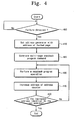
- operations begin at block 400 by determining if a program/read failure has been detected during a programming/reading operation of the non-volatile memory device. If a program/read failure has not be detected (block 400), operations remain at block 400 until a program/read failure has been detected. If, on the other hand, a program/read failure has been detected (block 400), operation proceed to block 410 where an address of a page of one of the memory blocks at which the failure was detected is stored (or set).
- the memory controller 250 may be configured to set the address of the failed page in the register 325 of the address generator 330.
- a multi-page copyback program command may be generated (block 420). As discussed above, the multi-page copyback command may be received from a host 290 at the memory controller 250. The memory controller 250 may provide the command to the program/read controller 255 of the control unit 220. The multi-page copyback program may be executed responsive to the multi-page copyback command.
- the multi-page copyback program includes blocks 430-450 of the flowchart of Figure 4.
- a page of data of the memory block having a first address may be replaced responsive to the generated multi-page copyback program command (block 430).
- the address in the counter of the address generator is incremented (block 440) and it is determined if the increased address of the page of data is the same as the stored address of the page at which the failure was detected (block 450). If it is determined that the addresses are the same (block 450), operations cease. If, on the other hand, it is determined that the addresses are not the same, operations of block 430 through 450 are repeated until it is determined at block 450 that the addresses are the same.
- operations of replacing may include determining a status of the replaced page as illustrated by the timing diagram of Figure 8. Furthermore, in some embodiments, before the operation of blocks 430-450 are repeated, a status of all of the replaced pages may be determined as illustrated by the timing diagram of Figure 6. In still further embodiments of the present invention, the step of incrementing (block 440) may be followed by suspending the multi-page copyback program and/or resuming the suspended multi-page copyback program which can be performed by the suspend and resume circuit 1187 of Figure 11 as will be discussed further below.
- a status read operation may be performed over the whole block. Furthermore, as illustrated in the timing diagram of Figure 8, a status read operation may be performed after each page. Finally, as illustrated by the timing diagram of Figure 7, a status read operation may be performed when program/read failure is detected.
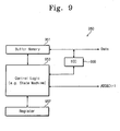
- the memory controller 950 may include control logic 953, a memory buffer 951, an error correction circuit (ECC) 959 and a register 957.
- the control logic 953 may be provided by, for example, a state machine without departing from the scope of the present invention.
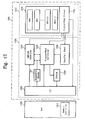
- Figures 10 through 12 are block diagrams illustrating flash memory devices in accordance with various embodiments of the present invention. It will be understood that the block diagrams of Figures 10 through 12 are similar to the block diagram discussed above with respect to Figure 2, thus like references numerals refer to like elements therein. In the interest of brevity only the differences will be discussed with respect to Figure 10 through 12.
- the memory controller 1050 may be provided at the host 1090 and replaced with an interface 1095 in the control unit 1020.
- the interface can be any interface known to those of skill in the art that can operate in accordance with embodiments of the present invention.
- a suspend and resume circuit 1187 may be provided in the control unit 1120.
- the suspend and resume circuit 1187 may be coupled to the memory controller 1150 and be configured to suspend and/or resume replacement operations as discussed above with respect to the flowchart of Figure 4.
- Figures 10 and 11 may also be combined to provide a memory controller 1250 in the host 1290 and a control unit 1220 including a suspend and resume circuit 1287.
- a system 1300 may include a microprocessor 1310, a user interface 1320, a modem 1350, a non-volatile memory device 1340 and an optional batter 1330 electrically coupled by a bus 1375.
- the user interface 1320 may include any man machine interface known to those having skill in the art. For example, a keypad, a touch screen, a voice activated circuit or the like. Furthermore, according to some embodiments of the present invention, the system 1300 may be included in a portable electronic device.
- the term "portable electronic device” or “mobile terminal” may include: a cellular radiotelephone with or without a multi-line display; a Personal Communications System (PCS) terminal that may combine a cellular radiotelephone with data processing, facsimile and data communications capabilities; a Personal Data Assistant (PDA) that can include a radiotelephone, pager, Internet/intranet access, Web browser, organizer, calendar and/or a global positioning system (GPS) receiver; a gaming device, an audio video player, and a conventional laptop and/or palmtop portable computer that may include a radiotelephone transceiver.
- PCS Personal Communications System
- PDA Personal Data Assistant
- gaming device an audio video player
- a conventional laptop and/or palmtop portable computer may include a radiotelephone transceiver.
- the non-volatile memory device may include a memory and a control unit as discussed above with respect to Figure 3.
- the memory may include one or more memory blocks including a plurality of pages of data.
- the control unit may be configured to execute a multi-page copyback command received from a host responsive to a program/read failure of a page of data in the one or more memory blocks.
- the failed page may have an associated failed page address and the multi-page copyback command is configured to initiate a replacement process for at least one of the plurality of pages of data until the failed page address is reached.
- FIG 14 a schematic block diagram illustrating systems according to some embodiments of the present invention will be discussed.
- the system 1400 is similar to the system of Figure 13 except the non-volatile memory 1465 and the control unit 1460 are separate.
Landscapes
- Engineering & Computer Science (AREA)
- Theoretical Computer Science (AREA)
- Computer Hardware Design (AREA)
- Physics & Mathematics (AREA)
- General Engineering & Computer Science (AREA)
- General Physics & Mathematics (AREA)
- Techniques For Improving Reliability Of Storages (AREA)
- Read Only Memory (AREA)
Priority Applications (1)
| Application Number | Priority Date | Filing Date | Title |
|---|---|---|---|
| US11/843,902 US7684241B2 (en) | 2006-08-28 | 2007-08-23 | Flash memory devices having multi-page copyback functionality and related block replacement methods |
Applications Claiming Priority (1)
| Application Number | Priority Date | Filing Date | Title |
|---|---|---|---|
| KR1020060081740A KR100837274B1 (ko) | 2006-08-28 | 2006-08-28 | 오토 멀티-페이지 카피백 기능을 갖는 플래시 메모리 장치및 그것의 블록 대체 방법 |
Publications (2)
| Publication Number | Publication Date |
|---|---|
| EP1895542A2 true EP1895542A2 (fr) | 2008-03-05 |
| EP1895542A3 EP1895542A3 (fr) | 2008-10-22 |
Family
ID=38780067
Family Applications (1)
| Application Number | Title | Priority Date | Filing Date |
|---|---|---|---|
| EP07016257A Withdrawn EP1895542A3 (fr) | 2006-08-28 | 2007-08-20 | Dispositif de mémoire flash doté de fonctionnalités de réintroductions multi-page et procédés de remplacement de blocs correspondants |
Country Status (4)
| Country | Link |
|---|---|
| US (1) | US7684241B2 (fr) |
| EP (1) | EP1895542A3 (fr) |
| KR (1) | KR100837274B1 (fr) |
| CN (1) | CN101221812B (fr) |
Cited By (1)
| Publication number | Priority date | Publication date | Assignee | Title |
|---|---|---|---|---|
| EP2636040A4 (fr) * | 2010-11-02 | 2015-03-18 | Micron Technology Inc | Opérations de réécriture |
Families Citing this family (13)
| Publication number | Priority date | Publication date | Assignee | Title |
|---|---|---|---|---|
| JP2009080884A (ja) * | 2007-09-26 | 2009-04-16 | Panasonic Corp | 不揮発性半導体記憶装置 |
| US8271515B2 (en) * | 2008-01-29 | 2012-09-18 | Cadence Design Systems, Inc. | System and method for providing copyback data integrity in a non-volatile memory system |
| KR101044533B1 (ko) * | 2009-06-29 | 2011-06-27 | 주식회사 하이닉스반도체 | 불휘발성 메모리 장치 및 이것의 카피백 프로그램 방법 |
| US8443263B2 (en) * | 2009-12-30 | 2013-05-14 | Sandisk Technologies Inc. | Method and controller for performing a copy-back operation |
| US8726104B2 (en) * | 2011-07-28 | 2014-05-13 | Sandisk Technologies Inc. | Non-volatile memory and method with accelerated post-write read using combined verification of multiple pages |
| US9158621B2 (en) * | 2011-08-29 | 2015-10-13 | Sandisk Technologies Inc. | System and method of copying data |
| CN104246694B (zh) * | 2011-12-29 | 2019-01-01 | 英特尔公司 | 聚集页错误信令和处理 |
| KR102072449B1 (ko) | 2012-06-01 | 2020-02-04 | 삼성전자주식회사 | 불휘발성 메모리 장치를 포함하는 저장 장치 및 그것의 리페어 방법 |
| KR102025088B1 (ko) | 2012-09-03 | 2019-09-25 | 삼성전자 주식회사 | 메모리 컨트롤러 및 상기 메모리 컨트롤러를 포함하는 전자장치 |
| KR20160061703A (ko) | 2014-11-24 | 2016-06-01 | 삼성전자주식회사 | 내부 카피 동작을 수행하는 메모리 장치 |
| CN107977282B (zh) * | 2017-12-20 | 2021-01-26 | 北京兆易创新科技股份有限公司 | 一种SPI-Nand读取数据页的方法及装置 |
| CN112131222B (zh) * | 2020-09-22 | 2024-04-02 | 深圳赛安特技术服务有限公司 | 消息读取状态数据的存储方法、装置、介质及电子设备 |
| US12072762B2 (en) * | 2022-08-09 | 2024-08-27 | Micron Technology, Inc. | Error-handling management during copyback operations in memory devices |
Citations (1)
| Publication number | Priority date | Publication date | Assignee | Title |
|---|---|---|---|---|
| US6813184B2 (en) | 2002-01-12 | 2004-11-02 | Samsung Electronics Co., Ltd. | NAND flash memory and method of erasing, programming, and copy-back programming thereof |
Family Cites Families (13)
| Publication number | Priority date | Publication date | Assignee | Title |
|---|---|---|---|---|
| US4520441A (en) * | 1980-12-15 | 1985-05-28 | Hitachi, Ltd. | Data processing system |
| JP3323869B2 (ja) * | 1992-03-31 | 2002-09-09 | 株式会社東芝 | 不揮発性半導体メモリ装置 |
| KR0172366B1 (ko) * | 1995-11-10 | 1999-03-30 | 김광호 | 불휘발성 반도체 메모리 장치의 독출 및 프로그램 방법과 그 회로 |
| JP2003030993A (ja) * | 2001-07-17 | 2003-01-31 | Toshiba Corp | 半導体記憶装置 |
| US6671204B2 (en) | 2001-07-23 | 2003-12-30 | Samsung Electronics Co., Ltd. | Nonvolatile memory device with page buffer having dual registers and methods of using the same |
| KR100447224B1 (ko) * | 2001-09-20 | 2004-09-04 | 주식회사 하이닉스반도체 | 비휘발성 강유전체 메모리 장치의 칼럼 리페어 회로 |
| JP3802411B2 (ja) | 2001-12-20 | 2006-07-26 | 株式会社東芝 | 不揮発性半導体記憶装置のデータコピー方法 |
| KR20040008717A (ko) * | 2002-07-19 | 2004-01-31 | 주식회사 하이닉스반도체 | 플래시 메모리 장치 |
| JP2004227723A (ja) | 2003-01-27 | 2004-08-12 | Renesas Technology Corp | 不揮発性半導体記憶装置 |
| JP4563715B2 (ja) * | 2003-04-29 | 2010-10-13 | 三星電子株式会社 | パーシャルコピーバック動作モードを有するフラッシュメモリ装置 |
| US20050005058A1 (en) * | 2003-07-01 | 2005-01-06 | Wee-Kuan Gan | Interleaving management method for upgrading data processing speed |
| KR100572328B1 (ko) * | 2004-07-16 | 2006-04-18 | 삼성전자주식회사 | 배드 블록 관리부를 포함하는 플래시 메모리 시스템 |
| US7187583B2 (en) * | 2005-01-25 | 2007-03-06 | Phison Electronics Corp. | Method for reducing data error when flash memory storage device using copy back command |
-
2006
- 2006-08-28 KR KR1020060081740A patent/KR100837274B1/ko active Active
-
2007
- 2007-08-20 EP EP07016257A patent/EP1895542A3/fr not_active Withdrawn
- 2007-08-23 US US11/843,902 patent/US7684241B2/en active Active
- 2007-08-28 CN CN2007103051503A patent/CN101221812B/zh active Active
Patent Citations (1)
| Publication number | Priority date | Publication date | Assignee | Title |
|---|---|---|---|---|
| US6813184B2 (en) | 2002-01-12 | 2004-11-02 | Samsung Electronics Co., Ltd. | NAND flash memory and method of erasing, programming, and copy-back programming thereof |
Cited By (1)
| Publication number | Priority date | Publication date | Assignee | Title |
|---|---|---|---|---|
| EP2636040A4 (fr) * | 2010-11-02 | 2015-03-18 | Micron Technology Inc | Opérations de réécriture |
Also Published As
| Publication number | Publication date |
|---|---|
| US20080068886A1 (en) | 2008-03-20 |
| CN101221812B (zh) | 2012-04-18 |
| CN101221812A (zh) | 2008-07-16 |
| KR100837274B1 (ko) | 2008-06-11 |
| EP1895542A3 (fr) | 2008-10-22 |
| KR20080019421A (ko) | 2008-03-04 |
| US7684241B2 (en) | 2010-03-23 |
Similar Documents
| Publication | Publication Date | Title |
|---|---|---|
| US7684241B2 (en) | Flash memory devices having multi-page copyback functionality and related block replacement methods | |
| US11756627B2 (en) | Semiconductor memory device | |
| CN107402832B (zh) | 存储器刷新方法及设备 | |
| CN101496109B (zh) | 具有多块擦除模式的非易失性存储器及其方法 | |
| US7889592B2 (en) | Non-volatile memory device and a method of programming the same | |
| KR101359765B1 (ko) | 메모리 소거 방법들과 디바이스들 | |
| CN101800078B (zh) | 一种非易失存储器的擦除方法及装置 | |
| US20090185421A1 (en) | Charge-Trap Flash Memory Device with Reduced Erasure Stress and Related Programming and Erasing Methods Thereof | |
| KR20030009288A (ko) | 누설 셀의 검출 및 복구를 외부에서 트리거하는 플래시메모리 | |
| CN101162610A (zh) | 对非易失性存储器件生成编程电压的电路和方法 | |
| WO2008136568A1 (fr) | Dispositif de programmation multibits et procédé de programmation associé | |
| CN101923900A (zh) | 一种非易失存储器的擦除方法及装置 | |
| CN101421793B (zh) | Nand存储器装置列充电 | |
| KR100845530B1 (ko) | 플래시 메모리 장치 및 그것의 동작 방법 | |
| US20080094927A1 (en) | Flash memory device with word line discharge unit and data read method thereof | |
| CN121483340A (zh) | 存储器的操作方法、存储器、存储器系统及电子设备 | |
| JP5378664B2 (ja) | マルチ−ページコピーバック機能を有するフラッシュメモリー装置及びそのブロック置換方法 | |
| KR100572333B1 (ko) | 데이터 라인을 간단하게 디스차지할 수 있는 노어 플래시메모리 장치 | |
| KR100842752B1 (ko) | 리드 디스터브가 억제되는 낸드 플래시 메모리소자의리드방법 | |
| US6233178B1 (en) | Method and apparatus for pre-conditioning flash memory devices | |
| US20100332736A1 (en) | Method of operating nonvolatile memory device | |
| KR20100076692A (ko) | 낸드 플래시 메모리소자 및 쓰기 방법 | |
| CN110908825A (zh) | 一种数据读取方法、装置、存储设备及存储介质 | |
| CN119479716A (zh) | 存储器装置和存储器装置的操作方法 | |
| KR20080062720A (ko) | 낸드 플래시 메모리소자의 프로그램 방법 |
Legal Events
| Date | Code | Title | Description |
|---|---|---|---|
| PUAI | Public reference made under article 153(3) epc to a published international application that has entered the european phase |
Free format text: ORIGINAL CODE: 0009012 |
|
| AK | Designated contracting states |
Kind code of ref document: A2 Designated state(s): AT BE BG CH CY CZ DE DK EE ES FI FR GB GR HU IE IS IT LI LT LU LV MC MT NL PL PT RO SE SI SK TR |
|
| AX | Request for extension of the european patent |
Extension state: AL BA HR MK YU |
|
| PUAL | Search report despatched |
Free format text: ORIGINAL CODE: 0009013 |
|
| AK | Designated contracting states |
Kind code of ref document: A3 Designated state(s): AT BE BG CH CY CZ DE DK EE ES FI FR GB GR HU IE IS IT LI LT LU LV MC MT NL PL PT RO SE SI SK TR |
|
| AX | Request for extension of the european patent |
Extension state: AL BA HR MK RS |
|
| RIC1 | Information provided on ipc code assigned before grant |
Ipc: G11C 16/34 20060101ALI20080917BHEP Ipc: G11C 11/56 20060101ALI20080917BHEP Ipc: G11C 16/10 20060101AFI20071211BHEP |
|
| 17P | Request for examination filed |
Effective date: 20090326 |
|
| 17Q | First examination report despatched |
Effective date: 20090427 |
|
| AKX | Designation fees paid |
Designated state(s): DE |
|
| GRAP | Despatch of communication of intention to grant a patent |
Free format text: ORIGINAL CODE: EPIDOSNIGR1 |
|
| STAA | Information on the status of an ep patent application or granted ep patent |
Free format text: STATUS: THE APPLICATION IS DEEMED TO BE WITHDRAWN |
|
| 18D | Application deemed to be withdrawn |
Effective date: 20100427 |