EP1895593B1 - Affichage électroluminescent organique - Google Patents
Affichage électroluminescent organique Download PDFInfo
- Publication number
- EP1895593B1 EP1895593B1 EP07253445.6A EP07253445A EP1895593B1 EP 1895593 B1 EP1895593 B1 EP 1895593B1 EP 07253445 A EP07253445 A EP 07253445A EP 1895593 B1 EP1895593 B1 EP 1895593B1
- Authority
- EP
- European Patent Office
- Prior art keywords
- conductive lines
- light emitting
- organic light
- insulation layer
- region
- Prior art date
- Legal status (The legal status is an assumption and is not a legal conclusion. Google has not performed a legal analysis and makes no representation as to the accuracy of the status listed.)
- Active
Links
Images
Classifications
-
- H—ELECTRICITY
- H10—SEMICONDUCTOR DEVICES; ELECTRIC SOLID-STATE DEVICES NOT OTHERWISE PROVIDED FOR
- H10K—ORGANIC ELECTRIC SOLID-STATE DEVICES
- H10K59/00—Integrated devices, or assemblies of multiple devices, comprising at least one organic light-emitting element covered by group H10K50/00
- H10K59/10—OLED displays
- H10K59/12—Active-matrix OLED [AMOLED] displays
- H10K59/131—Interconnections, e.g. wiring lines or terminals
-
- H—ELECTRICITY
- H05—ELECTRIC TECHNIQUES NOT OTHERWISE PROVIDED FOR
- H05B—ELECTRIC HEATING; ELECTRIC LIGHT SOURCES NOT OTHERWISE PROVIDED FOR; CIRCUIT ARRANGEMENTS FOR ELECTRIC LIGHT SOURCES, IN GENERAL
- H05B33/00—Electroluminescent light sources
- H05B33/12—Light sources with substantially two-dimensional [2D] radiating surfaces
- H05B33/26—Light sources with substantially two-dimensional [2D] radiating surfaces characterised by the composition or arrangement of the conductive material used as an electrode
-
- H—ELECTRICITY
- H10—SEMICONDUCTOR DEVICES; ELECTRIC SOLID-STATE DEVICES NOT OTHERWISE PROVIDED FOR
- H10K—ORGANIC ELECTRIC SOLID-STATE DEVICES
- H10K50/00—Organic light-emitting devices
- H10K50/80—Constructional details
- H10K50/84—Passivation; Containers; Encapsulations
- H10K50/841—Self-supporting sealing arrangements
-
- H—ELECTRICITY
- H10—SEMICONDUCTOR DEVICES; ELECTRIC SOLID-STATE DEVICES NOT OTHERWISE PROVIDED FOR
- H10K—ORGANIC ELECTRIC SOLID-STATE DEVICES
- H10K59/00—Integrated devices, or assemblies of multiple devices, comprising at least one organic light-emitting element covered by group H10K50/00
- H10K59/80—Constructional details
- H10K59/87—Passivation; Containers; Encapsulations
- H10K59/871—Self-supporting sealing arrangements
Definitions
- the present invention relates to an organic light emitting display, and more particularly, to an organic light emitting display in which signal lines disposed under a non-display region located out of a display region where an image is displayed, more specifically, a chip on glass (COG) region are prevented from being shorted.
- COG chip on glass
- CTR cathode ray tube
- a flat display device typically includes a liquid crystal display (LCD), a field emission display (FED), a plasma display panel (PDP), an organic light emitting display (OLED), and the like.
- LCD liquid crystal display
- FED field emission display
- PDP plasma display panel
- OLED organic light emitting display
- An organic light emitting display displays an image by driving N x M organic light emitting devices, which are emissive display elements for electrically exciting an organic compound to emit light, by using a voltage or current.
- an organic light emitting device may also be referred to as an organic light emitting diode.
- An organic light emitting device includes an anode electrode that is a hole injection electrode, an organic thin film that is a light emitting layer, and a cathode electrode that is an electron injection electrode.
- OLEDs including an organic light emitting device having the aforementioned structure can be classified into a passive matrix type OLED and an active matrix type OLED depending upon the driving type.
- An active matrix type OLED includes a first substrate provided with organic light emitting devices.
- the first substrate may be a driving circuit substrate including a driving circuit unit provided with TFTs.
- the first substrate may be a display substrate not provided with the driving circuit unit, hereinafter, it is assumed that the first substrate is the driving circuit substrate.
- the first substrate includes a display region, which is provided with organic light emitting devices, for displaying a predetermined image and a non-display region located outside the display region.
- the display region is provided with a lower structure.
- a flattening layer is formed on the lower structure.
- the lower structure includes a plurality of thin film transistors and an interlayer insulation film for insulating the gate electrodes of the thin film transistors from the source and drain electrodes thereof.
- an anode electrode electrically connected to the source and/or drain electrodes is formed on the flattening layer.
- the light emitting layer and a cathode electrode are sequentially formed on the anode electrode.
- the organic light emitting device including the anode electrode, the light emitting layer, and the cathode electrode is separated from a neighboring sub-pixel by using a pixel defining layer.
- the sub-pixel generally includes the light emitting layer for emitting red, green, or blue light.
- a single pixel includes three sub-pixels for emitting light of each color of R, G and B. Full colors can be displayed by using a plurality of pixel.
- the aforementioned organic light emitting display includes one or more driving ICs.
- the driving ICs may be generally mounted by a tape automated bonding (TAB) or by a chip on glass (COG) method.
- TAB tape automated bonding
- COG chip on glass
- the TAB method is a technique of mounting a tape carrier package (TCP) in which the driving IC is mounted, on the substrate
- the COG method is a technique of directly mounting the driving IC on the substrate.
- a driving IC having a finer pitch can be mounted as compared with a pitch used for the TAB method. Accordingly, recently, the COG method has been widely used.
- the COG region on which the driving IC is mounted has to be included on the substrate.
- a part of the non-display region disposed outside of the display region was used as the COG region.
- a plurality of organic light emitting displays are formed on a mother glass, all the organic light emitting displays are enclosed by using encapsulation glass, and the encapsulation glass and the mother glass are cut in units of displays to provide a plurality of displays.
- the COG type organic light emitting display is manufactured in the multi-panel process, a part of the encapsulation glass is scribed and removed to expose the COG region, and the driving IC is mounted on the exposed COG region.
- the present invention sets out to provide an organic light emitting display capable of preventing wires disposed on a non-display region from being shorted.
- an organic light emitting display device as set out in claim 1.
- Preferred features are set out in claims 2 to 10. Different signals may be transmitted through the first and second signal lines, respectively.
- the same signals may be transmitted through the first signal lines, and similarly, the same signals may be transmitted through the second signal lines.
- the signal lines are prevented from being shorted. Accordingly, serious errors are prevented from occurring in driving the organic light emitting devices.
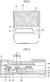
- the organic light emitting display includes first and second substrates 10 and 20 facing each other.
- the first substrate 10 may be made of transparent glass, opaque resin, or metal foil.
- the second substrate 20 enclosed in the first substrate 10 by using a sealant may be made of transparent glass or metal cap.
- the aforementioned structure may be sealed by coating the structure of the first substrate 10 with a thin film.
- the first substrate 10 includes a display region A1 and a non-display region A2.
- the display region A1 is provided with a plurality of organic light emitting devices 18 for displaying a predetermined image.
- FIG. 2 is a cross-sectional view illustrating an active matrix type organic light emitting display serving as a bottom emission type device.
- a buffer film 12 is formed on the first substrate 10, and thin film transistors 14 constituting a driving circuit unit are formed on the buffer film 12.
- a semiconductor layer 14a is formed on the buffer layer 12, and a gate insulation film 14b is formed on the semiconductor layer 14a and the buffer layer 12.
- the semiconductor 14a is formed by patterning a polycrystalline silicon film into a predetermined shape and injecting impurities into the polycrystalline silicon film to form source and drain regions and a channel region interposed therebetween.
- a gate electrode 14c is formed on the gate insulation film 14b, an interlayer insulation film 14d is formed on the gate electrode 14c and the gate insulation film 14b, and source and drain electrodes 14e and 14f are formed on the interlayer insulation film 14d.
- the source and drain electrodes 14e and 14f are electrically connected to the source and drain regions of the semiconductor layer 14a, respectively, through a connection hole of the interlayer insulation film 14d.
- a flattening layer 16 is formed on the thin film transistor 14 and the interlayer insulation film 14d, and an organic light emitting device 18 is formed on the flattening layer 16.
- an anode electrode 18a is formed on the flattening layer 16.
- the anode electrode 18a is electrically connected to the drain electrode 14f through a connection hole of the flattening layer 16.
- a light emitting layer 18b and a cathode electrode 18c are sequentially formed on the anode electrode 18a.
- the anode electrode 18a may be made of a transparent conductive material such as ITO or IZO to display light emitted from the light emitting layer 18b to the outside of the organic light emitting devices 18 through the anode electrode 18a and the first substrate 10.
- the organic light emitting devices 18 including the anode and cathode electrodes 18a and 18c and the light emitting layer 18b are separated from neighboring elements by a pixel defining layer 18d.
- the light emitting layer 18b may be constructed as a multilayer structure including a hole injection layer, a hole transport layer, and an electron transport layer to display one color of red, green, and blue.
- an electron injection layer may be further formed between the electron transport layer and the cathode electrode 18c.
- the organic light emitting devices 18 having the aforementioned structure display a predetermined image by allowing the light emitted from the light emitting layer 18b to pass through the anode electrode 18a and the first substrate 10 and to be emitted to the outside of the organic light emitting devices 18.
- a detailed structure of the aforementioned organic light emitting device and the thin film transistor may be changed according to a product specification.
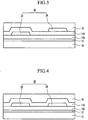
- the non-display region A2 disposed outside of the display region A1 includes a wiring section 30 for supplying a driving signal to the thin film transistor 14 or organic light emitting device 18.
- the wiring section 30 includes a plurality of signal lines 32 and 34.
- the driving signal is transmitted through the signal lines 32 and 34.
- the signal lines 32 and 34 which are made of the same material as the source and drain electrodes 14e and 14f, have been formed on the interlayer insulation film 16.
- the wiring section 30 includes a first signal line 32 formed on the gate insulation film 14b and a second signal line 34 formed on the interlayer insulation film 14d.
- first signal line 32 and one second signal line 34 are shown in FIG. 3 , a plurality of first signal lines 32 and a plurality of second signal lines 34 are formed under the COG region A3 in the same pattern as FIG. 3 , in practice.
- the first signal line 32 may be made of the same material as the gate electrode 14c.
- the second signal line 34 may be made of the same material as the source and drain electrodes 14e and 14f.
- the wiring section 30 having the aforementioned structure is constructed so that different signals are transmitted through the first and second signal lines 32 and 34, respectively.
- the same signals or different signals may be transmitted through the aforementioned first signal lines 32, and the same signals may be transmitted through the second signal lines 34.
- the first and second signal lines 32 and 34 need not be alternately formed one by one.
- two or more first signal lines 32 protected by the interlayer insulation film 14d may be formed between the second signal lines 34.
- all the signal lines constituting the wiring section 30, that is, the first and second signal lines 32 and 34 are made of the same material as the gate electrode 14c and formed on the gate insulation film 14b.
- two or more different voltages are transmitted through the signal lines 32 and 34.
Landscapes
- Engineering & Computer Science (AREA)
- Microelectronics & Electronic Packaging (AREA)
- Electroluminescent Light Sources (AREA)
- Devices For Indicating Variable Information By Combining Individual Elements (AREA)
Claims (12)
- Dispositif d'affichage électroluminescent organique comprenant :un premier substrat (10) comprenant une surface supérieure ;un deuxième substrat (20) ;un réseau de pixels électroluminescents organiques (18) interposés entre le premier substrat et le deuxième substrat ;un transistor à couche mince (14) interposé entre le premier substrat et le réseau de pixels électroluminescents organiques, le transistor à couche mince comprenant une couche semi-conductrice (14a), une électrode de grille (14c), une électrode de source (14e) et une électrode de drain (14f), une couche d'isolation de grille (14b) agencée entre la couche semi-conductrice et l'électrode de grille, et une couche d'isolation intermédiaire (14d) agencée entre l'électrode de grille et les électrodes de source et de drain ;une pluralité de lignes conductrices (32 et 34) comprenant des premières lignes conductrices et des deuxièmes lignes conductrices, dans lequel les premières lignes conductrices sont formées directement sur la couche d'isolation de grille et les deuxièmes lignes conductrices sont formées sur la couche d'isolation intermédiaire ; etune région de puce sur verre (COG) qui ne se chevauche pas avec le réseau de pixels électroluminescents organiques, où les premières et deuxièmes lignes conductrices sont disposées dans la région de COG,
caractérisé en ce quela couche d'isolation de grille comprend un premier prolongement, etdans lequel les premières lignes conductrices sont interposées entre le premier prolongement de la couche d'isolation de grille et la couche d'isolation intermédiaire, où la couche d'isolation intermédiaire comprend un deuxième prolongement, et où les deuxièmes lignes conductrices sont interposées entre le deuxième prolongement de la couche d'isolation intermédiaire et le réseau de pixels électroluminescents organiques et les premières et deuxièmes lignes conductrices sont essentiellement parallèles entre elles et ne se chevauchent pas lorsqu'elles sont vues dans une direction essentiellement perpendiculaire à la surface supérieure. - Dispositif selon la revendication 1, dans lequel les premières lignes conductrices (32) sont réalisées en un même matériau que l'électrode de grille.
- Dispositif selon l'une quelconque des revendications précédentes, dans lequel les deuxièmes lignes conductrices (34) sont réalisées en un même matériau que les électrodes de source et de drain (14e et 14f).
- Dispositif selon l'une des revendications précédentes, dans lequel les premières lignes conductrices (32) et les deuxièmes lignes conductrices (34) sont disposées dans un ordre alternatif le long d'une direction essentiellement parallèle à la surface supérieure.
- Dispositif selon l'une des revendications précédentes, dans lequel les signaux transmis à travers les premières lignes conductrices (32) sont différents des signaux transmis à travers les deuxièmes lignes conductrices (34).
- Dispositif selon l'une des revendications précédentes, dans lequel le réseau de pixels électroluminescents organiques définit une région d'affichage confinée par les premier et deuxième substrats (10 et 20) le long d'une première direction essentiellement perpendiculaire à la surface supérieure et par une surface périmétrique le long d'une deuxième direction essentiellement parallèle à la surface supérieure, dans lequel la surface périmétrique s'étend entre les premier et deuxième substrats et est perpendiculaire à la surface supérieure.
- Dispositif selon la revendication 6, dans lequel le réseau de pixels électroluminescents organiques est prévu dans la région d'affichage, et dans lequel le transistor à couche mince (14) est prévu dans la région d'affichage.
- Dispositif selon la revendication 6 ou 7, dans lequel la pluralité de lignes conductrices sont prévues dans une région de non-affichage, dans lequel la région de non-affichage comprend une région entre les premier et deuxième substrats (10 et 20), et dans lequel la région de non-affichage renferme la surface périmétrique de la région d'affichage.
- Dispositif de la revendication 8, dans lequel la région de non-affichage comprend en outre une région de puce sur verre (COG), où la pluralité de lignes conductrices est formée dans la région de COG.
- Dispositif selon l'une des revendications précédentes, dans lequel les premières et deuxièmes lignes conductrices (32 et 34) sont destinées à transmettre des signaux au transistor à couche mince (14).
- Procédé de fabrication d'un dispositif d'affichage électroluminescent organique, le procédé comprenant le fait :de former une couche semi-conductrice (14a) sur un premier substrat (10) ;de former une couche d'isolation de grille (14b) qui comprend un premier prolongement sur la couche semi-conductrice ;de former une électrode de grille (14c) et des premières lignes conductrices (32) directement sur la couche d'isolation de grille ;de former une couche d'isolation intermédiaire (14d) qui comprend un deuxième prolongement sur l'électrode de grille et les premières lignes conductrices, où les premières lignes conductrices sont interposées entre le premier prolongement de la couche d'isolation de grille et la couche d'isolation intermédiaire ;de former des deuxièmes lignes conductrices (34) sur la couche d'isolation intermédiaire, où les premières et deuxièmes lignes conductrices sont essentiellement parallèles entre elles et ne se chevauchent pas lorsqu'elles sont vues dans une direction essentiellement perpendiculaire à la surface supérieure ;de former des électrodes de source et de drain (14e et 14f) sur la couche d'isolation intermédiaire ;de former une couche d'aplatissement (16) sur les électrodes de source et de drain ;de former un réseau de pixels électroluminescents organiques sur la couche d'aplatissement, où les deuxièmes lignes conductrices sont interposées entre le deuxième prolongement de la couche d'isolation intermédiaire et le réseau de pixels électroluminescents organiques ; etde former une région de puce sur verre (COG) qui ne se chevauche pas avec le réseau de pixels électroluminescents organiques, où les premières et deuxièmes lignes conductrices sont disposées dans la région de COG.
- Procédé selon la revendication 11, comprenant en outre le fait de former la couche d'aplatissement (16) sur les deuxièmes lignes conductrices (34).
Applications Claiming Priority (1)
| Application Number | Priority Date | Filing Date | Title |
|---|---|---|---|
| KR1020060083527A KR100814820B1 (ko) | 2006-08-31 | 2006-08-31 | 유기 발광 표시장치 |
Publications (3)
| Publication Number | Publication Date |
|---|---|
| EP1895593A2 EP1895593A2 (fr) | 2008-03-05 |
| EP1895593A3 EP1895593A3 (fr) | 2011-04-13 |
| EP1895593B1 true EP1895593B1 (fr) | 2017-05-10 |
Family
ID=38754549
Family Applications (1)
| Application Number | Title | Priority Date | Filing Date |
|---|---|---|---|
| EP07253445.6A Active EP1895593B1 (fr) | 2006-08-31 | 2007-08-31 | Affichage électroluminescent organique |
Country Status (5)
| Country | Link |
|---|---|
| US (1) | US8415676B2 (fr) |
| EP (1) | EP1895593B1 (fr) |
| JP (1) | JP2008058928A (fr) |
| KR (1) | KR100814820B1 (fr) |
| CN (1) | CN101136427B (fr) |
Families Citing this family (13)
| Publication number | Priority date | Publication date | Assignee | Title |
|---|---|---|---|---|
| TWI443629B (zh) | 2008-12-11 | 2014-07-01 | Sony Corp | 顯示裝置、其驅動方法及電子設備 |
| JP5309946B2 (ja) * | 2008-12-12 | 2013-10-09 | ソニー株式会社 | 表示装置および電子機器 |
| KR101885806B1 (ko) * | 2012-05-01 | 2018-08-06 | 엘지디스플레이 주식회사 | 액정표시장치 및 그 제조방법 |
| CN105334994A (zh) * | 2014-08-06 | 2016-02-17 | 上海和辉光电有限公司 | 一种oled触控显示面板 |
| JP6469427B2 (ja) * | 2014-12-03 | 2019-02-13 | 株式会社ジャパンディスプレイ | 表示装置 |
| KR102490881B1 (ko) * | 2014-12-26 | 2023-01-25 | 삼성디스플레이 주식회사 | 유기 발광 표시 장치 및 그 제조 방법 |
| CN104617106B (zh) | 2015-01-09 | 2017-12-08 | 京东方科技集团股份有限公司 | 一种阵列基板及显示装置 |
| CN105068349A (zh) * | 2015-09-16 | 2015-11-18 | 京东方科技集团股份有限公司 | 阵列基板、显示面板、显示装置以及阵列基板的制作方法 |
| KR102447828B1 (ko) * | 2015-12-22 | 2022-09-28 | 삼성디스플레이 주식회사 | 유기 발광 표시 장치 |
| KR102572719B1 (ko) * | 2018-04-03 | 2023-08-31 | 삼성디스플레이 주식회사 | 표시 장치 |
| KR102586042B1 (ko) * | 2018-04-06 | 2023-10-10 | 삼성디스플레이 주식회사 | 디스플레이 장치 |
| JP6707156B2 (ja) * | 2019-01-16 | 2020-06-10 | 株式会社ジャパンディスプレイ | 表示装置 |
| KR20220170385A (ko) * | 2021-06-22 | 2022-12-30 | 삼성디스플레이 주식회사 | 표시 장치 |
Family Cites Families (13)
| Publication number | Priority date | Publication date | Assignee | Title |
|---|---|---|---|---|
| JP2002258315A (ja) * | 2001-03-01 | 2002-09-11 | Display Technologies Inc | アレイ基板、及びこれを用いる液晶表示装置 |
| KR100461634B1 (ko) | 2002-04-15 | 2004-12-14 | 엘지.필립스 엘시디 주식회사 | 유기전계 발광소자와 그 제조방법 |
| JP2004140267A (ja) * | 2002-10-18 | 2004-05-13 | Semiconductor Energy Lab Co Ltd | 半導体装置およびその作製方法 |
| JP4572510B2 (ja) * | 2003-06-17 | 2010-11-04 | セイコーエプソン株式会社 | エレクトロルミネッセンス表示装置及び電子機器 |
| JP2005109223A (ja) * | 2003-09-30 | 2005-04-21 | Sanyo Electric Co Ltd | 半導体装置および表示装置 |
| KR100579184B1 (ko) * | 2003-11-24 | 2006-05-11 | 삼성에스디아이 주식회사 | 유기전계발광표시장치 |
| KR100659532B1 (ko) | 2003-11-28 | 2006-12-19 | 삼성에스디아이 주식회사 | 평판표시장치 및 그의 제조방법 |
| KR100557731B1 (ko) | 2003-12-27 | 2006-03-06 | 엘지.필립스 엘시디 주식회사 | 유기전계 발광소자와 그 제조방법 |
| KR100626009B1 (ko) * | 2004-06-30 | 2006-09-20 | 삼성에스디아이 주식회사 | 박막 트랜지스터 구조체 및 이를 구비하는 평판디스플레이 장치 |
| JP2006071861A (ja) * | 2004-09-01 | 2006-03-16 | Seiko Epson Corp | 電気光学装置及び電子機器 |
| KR101014172B1 (ko) * | 2004-09-13 | 2011-02-14 | 삼성전자주식회사 | 구동유닛 및 이를 갖는 표시장치 |
| JP2006208903A (ja) * | 2005-01-31 | 2006-08-10 | Seiko Epson Corp | 電気光学装置および電子機器 |
| KR20070003178A (ko) * | 2005-06-30 | 2007-01-05 | 엘지.필립스 엘시디 주식회사 | 액정표시소자 |
-
2006
- 2006-08-31 KR KR1020060083527A patent/KR100814820B1/ko not_active Expired - Fee Related
-
2007
- 2007-01-10 JP JP2007002394A patent/JP2008058928A/ja active Pending
- 2007-04-02 US US11/731,966 patent/US8415676B2/en active Active
- 2007-04-23 CN CN2007101044740A patent/CN101136427B/zh not_active Expired - Fee Related
- 2007-08-31 EP EP07253445.6A patent/EP1895593B1/fr active Active
Also Published As
| Publication number | Publication date |
|---|---|
| CN101136427A (zh) | 2008-03-05 |
| CN101136427B (zh) | 2010-06-09 |
| KR20080020261A (ko) | 2008-03-05 |
| US20080055212A1 (en) | 2008-03-06 |
| US8415676B2 (en) | 2013-04-09 |
| JP2008058928A (ja) | 2008-03-13 |
| EP1895593A2 (fr) | 2008-03-05 |
| EP1895593A3 (fr) | 2011-04-13 |
| KR100814820B1 (ko) | 2008-03-20 |
Similar Documents
| Publication | Publication Date | Title |
|---|---|---|
| US8415676B2 (en) | Organic light emitting display | |
| US12185605B2 (en) | Display device | |
| US8410682B2 (en) | Organic light emitting display and method of fabricating the same | |
| CN1658713B (zh) | 平板显示器 | |
| US7211938B2 (en) | Double-sided display device and method of fabricating the same | |
| CN105609529A (zh) | 窄边框大面积有机发光二极管显示器 | |
| EP3255674A1 (fr) | Afficheur | |
| CN1638540B (zh) | 有机电致发光显示器件 | |
| KR102938368B1 (ko) | 표시 장치 | |
| CN116940175A (zh) | 显示基板 | |
| US20240397777A1 (en) | Display Substrate and Manufacturing Method therefor, and Display Apparatus | |
| KR101274699B1 (ko) | 유기 발광 소자 | |
| KR101212700B1 (ko) | 유기전계발광소자 및 그 제조방법 | |
| KR100739649B1 (ko) | 유기 전계 발광 표시장치 및 이의 제조 방법 | |
| KR101641363B1 (ko) | 유기전계발광 표시장치 | |
| CN219999921U (zh) | 显示基板 | |
| KR100766933B1 (ko) | 평판 표시장치 | |
| KR100752377B1 (ko) | 유기 전계발광 표시장치 | |
| KR100726994B1 (ko) | 유기 전계발광 표시장치 및 그 제조방법 | |
| KR20250067379A (ko) | 표시 장치 | |
| KR20050104100A (ko) | 유기전계발광 소자 및 그 제조방법 | |
| CN119546126A (zh) | 显示面板及其制备方法、显示装置 | |
| KR100667357B1 (ko) | 유기 전계발광 표시소자 및 그 제조방법 | |
| JP2007065298A (ja) | 表示装置、アレイ基板、及びアレイ基板の製造方法 |
Legal Events
| Date | Code | Title | Description |
|---|---|---|---|
| PUAI | Public reference made under article 153(3) epc to a published international application that has entered the european phase |
Free format text: ORIGINAL CODE: 0009012 |
|
| 17P | Request for examination filed |
Effective date: 20070906 |
|
| AK | Designated contracting states |
Kind code of ref document: A2 Designated state(s): AT BE BG CH CY CZ DE DK EE ES FI FR GB GR HU IE IS IT LI LT LU LV MC MT NL PL PT RO SE SI SK TR |
|
| AX | Request for extension of the european patent |
Extension state: AL BA HR MK YU |
|
| RAP1 | Party data changed (applicant data changed or rights of an application transferred) |
Owner name: SAMSUNG MOBILE DISPLAY CO., LTD. |
|
| PUAL | Search report despatched |
Free format text: ORIGINAL CODE: 0009013 |
|
| AK | Designated contracting states |
Kind code of ref document: A3 Designated state(s): AT BE BG CH CY CZ DE DK EE ES FI FR GB GR HU IE IS IT LI LT LU LV MC MT NL PL PT RO SE SI SK TR |
|
| AX | Request for extension of the european patent |
Extension state: AL BA HR MK RS |
|
| AKX | Designation fees paid |
Designated state(s): DE FR GB |
|
| RAP1 | Party data changed (applicant data changed or rights of an application transferred) |
Owner name: SAMSUNG DISPLAY CO., LTD. |
|
| 17Q | First examination report despatched |
Effective date: 20131101 |
|
| RAP1 | Party data changed (applicant data changed or rights of an application transferred) |
Owner name: SAMSUNG DISPLAY CO., LTD. |
|
| GRAP | Despatch of communication of intention to grant a patent |
Free format text: ORIGINAL CODE: EPIDOSNIGR1 |
|
| INTG | Intention to grant announced |
Effective date: 20161123 |
|
| GRAS | Grant fee paid |
Free format text: ORIGINAL CODE: EPIDOSNIGR3 |
|
| GRAA | (expected) grant |
Free format text: ORIGINAL CODE: 0009210 |
|
| AK | Designated contracting states |
Kind code of ref document: B1 Designated state(s): DE FR GB |
|
| REG | Reference to a national code |
Ref country code: GB Ref legal event code: FG4D |
|
| REG | Reference to a national code |
Ref country code: DE Ref legal event code: R096 Ref document number: 602007050921 Country of ref document: DE |
|
| REG | Reference to a national code |
Ref country code: FR Ref legal event code: PLFP Year of fee payment: 11 |
|
| REG | Reference to a national code |
Ref country code: DE Ref legal event code: R097 Ref document number: 602007050921 Country of ref document: DE |
|
| PLBE | No opposition filed within time limit |
Free format text: ORIGINAL CODE: 0009261 |
|
| STAA | Information on the status of an ep patent application or granted ep patent |
Free format text: STATUS: NO OPPOSITION FILED WITHIN TIME LIMIT |
|
| 26N | No opposition filed |
Effective date: 20180213 |
|
| REG | Reference to a national code |
Ref country code: FR Ref legal event code: PLFP Year of fee payment: 12 |
|
| REG | Reference to a national code |
Ref country code: DE Ref legal event code: R079 Ref document number: 602007050921 Country of ref document: DE Free format text: PREVIOUS MAIN CLASS: H01L0027320000 Ipc: H10K0059000000 |
|
| P01 | Opt-out of the competence of the unified patent court (upc) registered |
Effective date: 20230515 |
|
| PGFP | Annual fee paid to national office [announced via postgrant information from national office to epo] |
Ref country code: DE Payment date: 20240722 Year of fee payment: 18 |
|
| PGFP | Annual fee paid to national office [announced via postgrant information from national office to epo] |
Ref country code: GB Payment date: 20240723 Year of fee payment: 18 |
|
| PGFP | Annual fee paid to national office [announced via postgrant information from national office to epo] |
Ref country code: FR Payment date: 20240723 Year of fee payment: 18 |
|
| REG | Reference to a national code |
Ref country code: DE Ref legal event code: R119 Ref document number: 602007050921 Country of ref document: DE |
|
| GBPC | Gb: european patent ceased through non-payment of renewal fee |
Effective date: 20250831 |