EP1895656A2 - Hochgeschwindigkeitskomparator mit hoher Verstärkung der mit niedrigem Strom arbeitet - Google Patents
Hochgeschwindigkeitskomparator mit hoher Verstärkung der mit niedrigem Strom arbeitet Download PDFInfo
- Publication number
- EP1895656A2 EP1895656A2 EP07114707A EP07114707A EP1895656A2 EP 1895656 A2 EP1895656 A2 EP 1895656A2 EP 07114707 A EP07114707 A EP 07114707A EP 07114707 A EP07114707 A EP 07114707A EP 1895656 A2 EP1895656 A2 EP 1895656A2
- Authority
- EP
- European Patent Office
- Prior art keywords
- transistor
- current
- transistors
- output
- comparator
- Prior art date
- Legal status (The legal status is an assumption and is not a legal conclusion. Google has not performed a legal analysis and makes no representation as to the accuracy of the status listed.)
- Withdrawn
Links
Images




Classifications
-
- H—ELECTRICITY
- H03—ELECTRONIC CIRCUITRY
- H03F—AMPLIFIERS
- H03F3/00—Amplifiers with only discharge tubes or only semiconductor devices as amplifying elements
- H03F3/45—Differential amplifiers
- H03F3/45071—Differential amplifiers with semiconductor devices only
- H03F3/45076—Differential amplifiers with semiconductor devices only characterised by the way of implementation of the active amplifying circuit in the differential amplifier
- H03F3/45179—Differential amplifiers with semiconductor devices only characterised by the way of implementation of the active amplifying circuit in the differential amplifier using MOSFET transistors as the active amplifying circuit
- H03F3/45183—Long tailed pairs
-
- H—ELECTRICITY
- H03—ELECTRONIC CIRCUITRY
- H03K—PULSE TECHNIQUE
- H03K5/00—Manipulating of pulses not covered by one of the other main groups of this subclass
- H03K5/22—Circuits having more than one input and one output for comparing pulses or pulse trains with each other according to input signal characteristics, e.g. slope, integral
- H03K5/24—Circuits having more than one input and one output for comparing pulses or pulse trains with each other according to input signal characteristics, e.g. slope, integral the characteristic being amplitude
- H03K5/2472—Circuits having more than one input and one output for comparing pulses or pulse trains with each other according to input signal characteristics, e.g. slope, integral the characteristic being amplitude using field effect transistors
- H03K5/2481—Circuits having more than one input and one output for comparing pulses or pulse trains with each other according to input signal characteristics, e.g. slope, integral the characteristic being amplitude using field effect transistors with at least one differential stage
-
- H—ELECTRICITY
- H03—ELECTRONIC CIRCUITRY
- H03F—AMPLIFIERS
- H03F2203/00—Indexing scheme relating to amplifiers with only discharge tubes or only semiconductor devices as amplifying elements covered by H03F3/00
- H03F2203/45—Indexing scheme relating to differential amplifiers
- H03F2203/45466—Indexing scheme relating to differential amplifiers the CSC being controlled, e.g. by a signal derived from a non specified place in the dif amp circuit
-
- H—ELECTRICITY
- H03—ELECTRONIC CIRCUITRY
- H03F—AMPLIFIERS
- H03F2203/00—Indexing scheme relating to amplifiers with only discharge tubes or only semiconductor devices as amplifying elements covered by H03F3/00
- H03F2203/45—Indexing scheme relating to differential amplifiers
- H03F2203/45648—Indexing scheme relating to differential amplifiers the LC comprising two current sources, which are not cascode current sources
-
- H—ELECTRICITY
- H03—ELECTRONIC CIRCUITRY
- H03F—AMPLIFIERS
- H03F2203/00—Indexing scheme relating to amplifiers with only discharge tubes or only semiconductor devices as amplifying elements covered by H03F3/00
- H03F2203/45—Indexing scheme relating to differential amplifiers
- H03F2203/45664—Indexing scheme relating to differential amplifiers the LC comprising one or more cascaded inverter stages as output stage at one output of the dif amp circuit
Definitions
- the present invention relates, in general, to a comparator. More specifically, the present invention relates to a high gain, high speed comparator that is operable with low current.
- a comparator may be implemented with an operational amplifier that compares two input voltages and provides an output signal to indicate which input voltage is larger.
- a comparator has an inverting input terminal and a non-inverting input terminal. When the non-inverting input terminal is at a higher voltage than the inverting input terminal, the gain of the operational amplifier causes the output signal to become positive. When the voltage of the non-inverting input terminal drops below the voltage of the inverting input terminal, the operational amplifier causes the output signal to drop towards a ground potential.
- a comparator is useful for a variety of functions, such as polarity identification, 1-bit analog-to-digital conversion, driving a switch, square/triangular-wave generation, and pulse-edge generation.
- a comparator In order to compare small voltage differences at the input terminals, a comparator requires a high gain. The comparator must also have a high gain to provide a fast transition at the output terminal. This is because the output signal of the comparator does not change instantaneously but experiences a propagation delay from the time of arrival of the two input signals at the input terminals. In order to increase the gain, however, amplification stages are typically added to conventional comparators, thereby increasing current draw and propagation delay. A conventional comparator disadvantageously draws a higher current, when the input voltages are near the switching threshold of the comparator, i.e. when the difference between the input voltages is small.
- the present invention provides a comparator including a differential pair of transistors for (a) providing a first stage of amplification and (b) receiving inverting and non-inverting input signals. Also included is an output transistor having a grounded node. The output transistor is coupled to the differential pair of transistors for (a) providing a second stage of amplification and (b) transitioning the output signal from one state to another state when the non-inverting input signal is larger than the inverting input signal.
- the output node of one of the differential pair of transistors is connected to the input node of a current-tail transistor.
- the output node of the other differential transistor is connected to an input node of the output transistor.
- the input nodes of the differential pair of transistors receive the inverting and non-inverting input signals to the comparator.
- the other nodes of the differential pair of transistors are connected to each other and are coupled to an output node of the current-tail transistor.
- the output nodes of the differential pair of transistors and an output node of the output transistor are each coupled to a separate current generator that includes a complex impedance element.
- These current generators may be implemented as a field effect transistor (FET), a bipolar transistor (BJT) or as passive complex impedance elements.
- FET field effect transistor
- BJT bipolar transistor
- the current generators may be biased by an externally supplied current or by a current flowing in an internal feedback transistor.
- the current generators provide currents of i1 and i2 to the output nodes, respectively, of the differential pair of transistors, thus providing a current of i3 to the output node of the current-tail transistor.
- the current i3 is substantially equal to the sum of currents i1 and i2.
- the current generators also provide a current of i5 to the output node of the output transistor, and the current of i5 mirrors the current of i3.
- each current generator includes a field effect transistor (FET) coupled to each respective output node, and the FET is biased by the current flowing in the feedback transistor.
- FET field effect transistor
- BJT bipolar transistor
- Yet another preferred embodiment of the present invention is the differential pair of transistors including two similar FETs or two similar bipolar transistors, with the output transistor and the current-tail transistor including proportionally sized FETs or proportionally sized bipolar transistors.
- the current-tail transistor is configured to have a current flow that is substantially equal to the sum of the currents flowing in each of the differential pair of transistors.
- the output transistor is configured to have a current flow that is proportional to the current flowing in the current-tail transistor.
- the present invention provides a comparator including a differential pair of transistors for (a) providing a first stage of amplification and (b) receiving inverting and non-inverting input signals. Also included is an output transistor having a grounded node. The output transistor is coupled to the differential pair of transistors for (a) providing a second stage of amplification and (b) transitioning the output signal from one state to another state when the non-inverting input signal is larger than the inverting input signal.
- the output nodes of the differential pair of transistors and the output node of the output transistor are each coupled to a separate current generator.
- Each current generator provides a separate current source to feed each of the differential pair of transistors and the output transistor.
- these current sources may be implemented with complex impedance elements which are connected directly to a power supply.
- these current sources may be implemented with field effect transistors (FETs), or with bipolar transistors (BJTs), which are biased by an externally provided current generator.
- FETs or the BJTs are biased by a current generated from an internally provided feedback transistor.
- Comparator 100 includes two voltage input signals, shown as Vin inverting and Vin non-inverting.
- the comparator 100 also includes an output signal shown as Vout.
- the comparator 100 may optionally include a biasing control, shown as I-bias external. This biasing control will be described later.
- comparator 100 includes a VCC power supply input of nominally 1.5 volts (for example) and a ground potential.
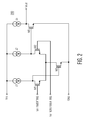
- comparator 200 includes a differential pair of transistors, designated as M1 and M2. Comparator 200 also includes a current-tail transistor, designated as M3, and an output transistor designated as M5. Although these transistors are shown implemented with field effect transistors (FETs), it will be appreciated that comparator 200 may be implemented with bipolar transistors (BJTs). Comparator 200 further includes current sources, designated as 11, 12 and 15. The 11 current source provides current to flow into the drain of transistor M1, the 12 current source provides current to flow into the drain of transistor M2, and the 15 current source provides current to flow into the drain of transistor M5.
- FETs field effect transistors
- BJTs bipolar transistors
- transistors M1 and M2 receive the inverting and non-inverting input signals of comparator 200, respectively. Together, transistors M1 and M2 provide a first stage of amplification for the comparator.
- the input signals, Vin inverting and Vin non-inverting, are coupled to the gates of transistors M1 and M2, respectively.
- the drain of transistor M1 is coupled to current source 11.
- the drain of transistor M2 is coupled to current source 12.
- Current sources 11 and 12 are each coupled to the power supply voltage VCC.
- the sources of differential transistor pair M1 and M2 are connected together, and are also connected to the drain of current-tail transistor M3.
- the gate of current-tail transistor M3 is connected to the drain of transistor M1 and the source of current-tail transistor M3 is grounded.
- the drain of transistor M2 is connected to the gate of output transistor M5.
- the drain of output transistor M5 is connected to current source 15.
- Current source 15 is also coupled to VCC.
- Output transistor M5 is connected in a common-source configuration, with its source connected to ground and with its drain providing the output, Vout, of comparator 200. In this manner, transistor M5 provides the second stage of amplification for comparator 200.
- comparator 300 includes the differential pair of transistors M1 and M2, the current-tail transistor M3, and the output transistor M5. Although these transistors are shown implemented with field effect transistors (FETs), it will be appreciated that comparator 300 may be implemented with bipolar transistors (BJTs).
- FETs field effect transistors
- BJTs bipolar transistors
- the current sources are implemented with complex impedance elements Z1, Z2 and Z5. These complex impedances may include some or all of the following elements: resistors, capacitors and inductors.
- the input signals, Vin inverting and Vin non-inverting are coupled to the gates of transistors M1 and M2, respectively.
- the drain of transistor M1 is coupled to complex impedance element Z1.
- the drain of transistor M2 is coupled to complex impedance element Z2.
- Complex impedance elements Z1 and Z2 are each coupled to the power supply voltage VCC.
- the values of complex impedance elements Z1 and Z2 determine, respectively, current i 1 and current i 2 . If element Z1 is equal to element Z2, current i 1 equals current i 2 .
- the sources of the differential transistor pair M1 and M2 in FIG. 3 are connected together, and are coupled to the drain of current-tail transistor M3.
- the gate of current-tail transistor M3 is coupled to the drain of transistor M1 and the source of current-tail transistor M3 is grounded.
- the drain of transistor M2 is connected to the gate of output transistor M5.
- the drain of output transistor M5 is coupled to complex impedance element Z5.
- Complex impedance element Z5 is also coupled to VCC.
- Output transistor M5 is connected in a common-source configuration, with its source connected to ground and with its drain providing the output, Vout, of comparator 300.
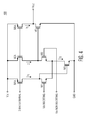
- comparator 400 includes the differential pair of transistors M1 and M2, the current-tail transistor M3, and the output transistor M5. Although these transistors are shown implemented with field effect transistors (FETs), it will be appreciated that comparator 400 may be implemented with bipolar transistors (BJTs). In the exemplary embodiment of FIG. 4, the current sources are implemented with bias transistors M1A, M2A and M5A.
- the input signals, Vin inverting and Vin non-inverting are coupled to the gates of transistors M1 and M2, respectively.
- the drain of transistor M1 is coupled to the drain of bias transistor M1A.
- the drain of M2 is coupled to the drain of bias transistor M2A.
- the drain of M5 is coupled to the drain of bias transistor M5A.
- the source of each bias transistor M1A, M2A and M5A is coupled to the power supply voltage VCC.
- the gates of bias transistors M1A, M2A and M5A are connected together and coupled to an external terminal for providing the I-bias external signal.
- the sources of the differential transistor pair M1 and M2 are connected together, and are coupled to the drain of current-tail transistor M3.
- the gate of current-tail transistor M3 is coupled to the drain of transistor M1 and the source of current-tail transistor M3 is grounded.
- the drain of transistor M2 is connected to the gate of output transistor M5.
- Output transistor M5 is connected in a common-source configuration, with its source connected to ground and with its drain providing the output, Vout, of comparator 400.
- transistors M1, M2, M3 and M5 are shown implemented using NMOS transistors. It will be appreciated that these transistors may also be implemented using NPN bipolar transistors.
- the transistors M1A, M2A and M5A are shown implemented using PMOS transistors. It will be appreciated that these transistors may also be implemented using PNP bipolar transistors.
- bias transistors M1A and M2A respectively, supply the currents i 1 and i 2 which flow, respectively, through differential transistor pair M1 and M2.
- the current i 3 flowing through current-tail transistor M3 is equal to the sum of current i 1 and current i 2 flowing through the differential transistor pair M1 and M2.
- the amount of drain current that bias transistors M1A and M2A can supply is determined by the I-bias external control signal.
- bias transistor M5A supplies the current i 5 and the amount of drain current that bias transistor M5A can supply is determined by the 1-bias external control signal.
- transistor M2 When the Vin non-inverting input signal is at a higher voltage than the Vin inverting input signal, transistor M2 has a higher gate to source voltage (Vgs) than transistor M1. Thus, transistor M2 is more saturated than transistor M1, and as a result, current i 2 is greater than current i 1 . Current i 3 is equal to the sum of currents i 1 and i 2 . Since transistor M1 is less saturated than transistor M2, the drain to source voltage (Vds) of transistor M1 increases, and, therefore, the gate to source voltage (Vgs) of current-tail transistor M3 increases.
- transistor M1 when the Vin inverting input signal is at a higher voltage than the Vin non-inverting input signal, transistor M1 has a higher gate to source voltage (Vgs) than transistor M2. Thus, transistor M1 conducts in a region that is more saturated than the region of conductance of transistor M2. As a result, current i 1 becomes greater than current i 2 . Current i 3 is equal to the sum of currents i 1 and i 2 .
- comparator 500 includes the differential pair of transistors M1 and M2, the current-tail transistor M3, and the output transistor M5. Although these transistors are shown implemented with field effect transistors (FETs), it will be appreciated that these transistors may also be implemented with bipolar transistors (BJTs).
- FETs field effect transistors
- BJTs bipolar transistors
- the current sources are implemented with transistors M1A, M2A and M5A.
- a feedback transistor M4 which has its own bias transistor M4A.
- the connections of the components comprising comparator 500 are similar to the connections of the components comprising comparator 200, 300, or 400. Accordingly, the input signals Vin inverting and Vin non-inverting are coupled to the gates of transistors M1 and M2, respectively.
- the drain of transistor M1 is coupled to the drain of bias transistor M1A.
- the drain of M2 is coupled to the drain of bias transistor M2A.
- the source of each of the bias transistors M1A, M2A and M5A is coupled to the power supply voltage VCC.
- the sources of the differential transistor pair M1 and M2 are connected together, and also coupled to the drain of current-tail transistor M3.
- the gate of current-tail transistor M3 is coupled to the drain of transistor M1 and the source of current-tail transistor M3 is grounded.
- the drain of transistor M2 is connected to the gate of output transistor M5.
- the drain of output transistor M5 is coupled to the drain of bias transistor M5A.
- Output transistor M5 is connected in a common-source configuration, with its source connected to ground and with its drain providing the output, Vout, of comparator 500.
- the gate of each of the bias transistors M1A, M2A and M5A are connected together and coupled for bias control by feedback transistor M4 and its current source transistor M4A.
- the control signal 1-bias external shown in FIG. 4 is replaced in FIG. 5 by the internal feedback loop of feedback transistor M4 and feedback bias transistor M4A.
- the drain of feedback transistor M4 is connected to the drain of bias transistor M4A.
- the source of feedback transistor M4 is grounded.
- the source of bias transistor M4A is connected to the power supply voltage VCC.
- the gate of feedback transistor M4 is coupled to the gate of current-tail transistor M3, and the gate of feedback bias transistor M4A is coupled to the gate of each bias transistor M1A, M2A and M5A.
- the gate and drain of feedback bias transistor M4A are coupled to each other forming a connected node, and permitting feedback transistor M4 to control the gate voltages of each of the bias transistors M1A, M2A, M4A and M5A.
- transistors M1, M2, M3, M4 and M5 are shown implemented using NMOS transistors. It will be appreciated that these transistors may also be implemented using NPN bipolar transistors.
- the transistors M1A, M2A, M4A and M5A are shown implemented using PMOS transistor. It will be appreciated that these transistors may also be implemented using PNP bipolar transistors.
- the current i 3 flowing through the current-tail transistor M3 is substantially equal to the sum of current i 1 and current i 2 flowing through the differential transistor pair M1 and M2.
- Bias transistors M1A and M2A respectively, supply the currents i 1 and i 2 .
- the drain current that bias transistors M1A and M2A can supply is determined by feedback transistor M4 and feedback bias transistor M4A, which will be described later.
- bias transistor M5A supplies the current i 5 , whose level is also determined by feedback transistor M4 and feedback bias transistor M4A.
- transistor M2 When the Vin non-inverting input signal is at a higher voltage than the Vin inverting input signal, transistor M2 has a higher gate to source voltage (Vgs) than transistor M1. Thus, transistor M2 is more saturated than transistor M1, and as a result, current i 2 is greater than current i 1 . Current i 3 is equal to the sum of currents i 1 and i 2 . Since transistor M1 is less saturated than transistor M2, the drain to source voltage (Vds) of transistor M1 increases and, therefore, the gate to source voltages (Vgs) of both current-tail transistor M3 and feedback transistor M4 also increase.
- Vds drain to source voltage
- the gate to source voltage (Vgs) of M4 is substantially equal to the gate to source voltage (Vgs) of current-tail transistor M3. Furthermore, the relationship between currents i 3 and i 4 is based upon the relationship between the physical sizes of transistors M3 and M4 and, accordingly, bias current i 4 substantially mirrors current i 3 . When the size of transistor M3 is N times the size of transistor M4, current i 3 is equal to N times current i 4 . When current-tail transistor M3 and feedback transistor M4 are of the same physical size, current i 4 is substantially equal to current i 3 , which is substantially equal to the sum of current i 1 and current i 2 .
- each bias transistor M1A, M2A, M4A and M5A is also substantially grounded. This creates a highly negative gate to source voltage (Vgs) on each of the bias transistors. Because each bias transistor is a PMOS transistor, as shown in FIG. 5, the highly negative gate to source voltage (Vgs) pushes each bias transistor into saturation, and increases currents i 1 , i 2 , i 4 and i 5 .
- transistor M1 when the Vin inverting input signal is at a higher voltage than the Vin non-inverting input signal, transistor M1 has a higher gate to source voltage (Vgs) than transistor M2. Thus, transistor M1 becomes more conducting than transistor M2, and as a result, current i 1 becomes greater than current i 2 . Current i 3 is equal to the sum of currents i 1 and i 2 . As transistor M1 becomes more saturated, the drain to source voltage (Vds) of transistor M1 decreases, and the gate to source voltages (Vgs) of both current-tail transistor M3 and feedback transistor M4 also decrease.
- Vds drain to source voltage
- Vgs gate to source voltages
- each bias transistor M1A, M2A, M4A and M5A has a positive voltage, which reduces the magnitude of the gate to source voltage (Vgs) on each of the bias transistors. Because each bias transistor is a PMOS transistor, as shown in FIG. 5, the reduction in the magnitude of each gate to source voltage (Vgs) decreases respective currents i 1 , i 2 , i 4 and i 5 .
- comparator 200 achieves a very short propagation delay between the time of the input of the two comparison signals and the time of the output signal toggle. This delay is represented by ⁇ t, and is of very short duration, such as approximately 0.5 ns.
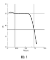
- FIG. 7 shows an exemplary logarithmic plot of gain versus frequency of comparator 200. As shown, comparator 200 achieves a high gain of approximately 50 dB, over a wide frequency range. This high gain is implemented with only two stages of amplification, thereby also achieving a very small propagation delay for the comparison.
Landscapes
- Engineering & Computer Science (AREA)
- Power Engineering (AREA)
- Physics & Mathematics (AREA)
- Nonlinear Science (AREA)
- Manipulation Of Pulses (AREA)
- Amplifiers (AREA)
Applications Claiming Priority (1)
| Application Number | Priority Date | Filing Date | Title |
|---|---|---|---|
| US11/514,121 US7579878B2 (en) | 2006-08-31 | 2006-08-31 | High gain, high speed comparator operable at low current |
Publications (2)
| Publication Number | Publication Date |
|---|---|
| EP1895656A2 true EP1895656A2 (de) | 2008-03-05 |
| EP1895656A3 EP1895656A3 (de) | 2008-12-24 |
Family
ID=38668781
Family Applications (1)
| Application Number | Title | Priority Date | Filing Date |
|---|---|---|---|
| EP20070114707 Withdrawn EP1895656A3 (de) | 2006-08-31 | 2007-08-21 | Hochgeschwindigkeitskomparator mit hoher Verstärkung der mit niedrigem Strom arbeitet |
Country Status (3)
| Country | Link |
|---|---|
| US (1) | US7579878B2 (de) |
| EP (1) | EP1895656A3 (de) |
| AU (1) | AU2007203544B2 (de) |
Families Citing this family (6)
| Publication number | Priority date | Publication date | Assignee | Title |
|---|---|---|---|---|
| US7825723B1 (en) * | 2009-03-09 | 2010-11-02 | Atheros Communications, Inc. | Method and apparatus using an I/O device to eliminate a level shifter in low-voltage CMOS integrated circuits |
| US9134741B2 (en) * | 2009-06-13 | 2015-09-15 | Triune Ip, Llc | Dynamic biasing for regulator circuits |
| JP5917858B2 (ja) * | 2011-08-29 | 2016-05-18 | ルネサスエレクトロニクス株式会社 | 半導体集積回路装置 |
| US9729140B2 (en) * | 2014-03-05 | 2017-08-08 | Analog Devices, Inc. | Circuits with floating bias |
| KR102679071B1 (ko) * | 2016-11-24 | 2024-07-01 | 에스케이하이닉스 주식회사 | 버퍼 회로, 이를 이용하는 반도체 장치 및 시스템 |
| JP7085911B2 (ja) * | 2018-06-15 | 2022-06-17 | エイブリック株式会社 | コンパレータ及び発振回路 |
Family Cites Families (14)
| Publication number | Priority date | Publication date | Assignee | Title |
|---|---|---|---|---|
| US4342004A (en) | 1979-05-15 | 1982-07-27 | Tokyo Shibaura Denki Kabushiki Kaisha | Voltage comparator circuit |
| JP2598074B2 (ja) | 1988-03-19 | 1997-04-09 | 富士通株式会社 | 演算増幅器 |
| GB2222497A (en) * | 1988-09-05 | 1990-03-07 | Philips Electronic Associated | Operational amplifier |
| US5596289A (en) * | 1995-05-15 | 1997-01-21 | National Science Council | Differential-difference current conveyor and applications therefor |
| US5614852A (en) | 1995-08-08 | 1997-03-25 | Harris Corp. | Wide common mode range comparator and method |
| US5990708A (en) * | 1997-02-03 | 1999-11-23 | Texas Instruments Incorporated | Differential input buffer using local reference voltage and method of construction |
| US6118318A (en) * | 1997-05-09 | 2000-09-12 | International Business Machines Corporation | Self biased differential amplifier with hysteresis |
| US5963053A (en) * | 1997-10-09 | 1999-10-05 | Pericom Semiconductor Corp. | Self-biasing CMOS PECL receiver with wide common-mode range and multi-level-transmit to binary decoder |
| US5939904A (en) * | 1998-02-19 | 1999-08-17 | Lucent Technologies, Inc. | Method and apparatus for controlling the common-mode output voltage of a differential buffer |
| US6507239B2 (en) | 2000-07-21 | 2003-01-14 | Ixys Corporation | Low noise and low offset bipolar input amplifiers |
| US6549049B1 (en) * | 2002-04-11 | 2003-04-15 | Texas Instruments Incorporated | Dynamic voltage reference circuit |
| US6864725B2 (en) * | 2002-06-05 | 2005-03-08 | Micron Technology, Inc. | Low current wide VREF range input buffer |
| KR100559406B1 (ko) * | 2004-10-15 | 2006-03-10 | 삼성전자주식회사 | 히스테리시스를 갖는 비교기 및 그것을 사용한 비교 방법 |
| US7595676B2 (en) * | 2007-07-23 | 2009-09-29 | Texas Instruments Incorporated | Comparator and method with controllable threshold and hysteresis |
-
2006
- 2006-08-31 US US11/514,121 patent/US7579878B2/en not_active Expired - Fee Related
-
2007
- 2007-07-30 AU AU2007203544A patent/AU2007203544B2/en not_active Ceased
- 2007-08-21 EP EP20070114707 patent/EP1895656A3/de not_active Withdrawn
Also Published As
| Publication number | Publication date |
|---|---|
| AU2007203544B2 (en) | 2011-07-28 |
| EP1895656A3 (de) | 2008-12-24 |
| US7579878B2 (en) | 2009-08-25 |
| AU2007203544A1 (en) | 2008-03-20 |
| US20080054949A1 (en) | 2008-03-06 |
Similar Documents
| Publication | Publication Date | Title |
|---|---|---|
| US6608526B1 (en) | CMOS assisted output stage | |
| US7397309B2 (en) | Bias circuit for a wideband amplifier driven with low voltage | |
| US7548117B2 (en) | Differential amplifier having an improved slew rate | |
| US6437645B1 (en) | Slew rate boost circuitry and method | |
| US6433637B1 (en) | Single cell rail-to-rail input/output operational amplifier | |
| US20050270077A1 (en) | Method and apparatus for providing a power-on reset signal | |
| US20090146624A1 (en) | Shunt regulator having over-voltage protection circuit and semiconductor device including the same | |
| CN103748786B (zh) | 具有共模反馈的宽带宽c类放大器 | |
| US6236270B1 (en) | Operational amplifier circuit including folded cascode circuit | |
| EP2047593B1 (de) | Stapelpuffer | |
| EP1895656A2 (de) | Hochgeschwindigkeitskomparator mit hoher Verstärkung der mit niedrigem Strom arbeitet | |
| US20050184805A1 (en) | Differential amplifier circuit | |
| TW201821925A (zh) | 穩壓器 | |
| US6545502B1 (en) | High frequency MOS fixed and variable gain amplifiers | |
| JP2019527981A (ja) | 選択可能な電流リミッタ回路 | |
| US7319365B2 (en) | Signal determining apparatus including amplifier circuit with variable response speed | |
| NL1029337A1 (nl) | Zelf ingestelde differentiele versterker. | |
| US20070024367A1 (en) | Operational amplifier and constant-current generation circuit using the same | |
| US6593769B1 (en) | Differential, reduced swing buffer design | |
| JP5974998B2 (ja) | 演算増幅器 | |
| JP2003046347A (ja) | 高出力増幅器 | |
| CN116232242A (zh) | Ab类输出级的偏置电路以及ab类放大器、芯片和电子设备 | |
| JP2004064132A (ja) | 演算増幅器 | |
| US7265621B1 (en) | Fully differential operational amplifier with fast settling time | |
| KR100668455B1 (ko) | 가변 이득 증폭기 |
Legal Events
| Date | Code | Title | Description |
|---|---|---|---|
| PUAI | Public reference made under article 153(3) epc to a published international application that has entered the european phase |
Free format text: ORIGINAL CODE: 0009012 |
|
| AK | Designated contracting states |
Kind code of ref document: A2 Designated state(s): AT BE BG CH CY CZ DE DK EE ES FI FR GB GR HU IE IS IT LI LT LU LV MC MT NL PL PT RO SE SI SK TR |
|
| AX | Request for extension of the european patent |
Extension state: AL BA HR MK YU |
|
| PUAL | Search report despatched |
Free format text: ORIGINAL CODE: 0009013 |
|
| AK | Designated contracting states |
Kind code of ref document: A3 Designated state(s): AT BE BG CH CY CZ DE DK EE ES FI FR GB GR HU IE IS IT LI LT LU LV MC MT NL PL PT RO SE SI SK TR |
|
| AX | Request for extension of the european patent |
Extension state: AL BA HR MK RS |
|
| 17P | Request for examination filed |
Effective date: 20090205 |
|
| AKX | Designation fees paid |
Designated state(s): DE FR GB |
|
| 17Q | First examination report despatched |
Effective date: 20111024 |
|
| RAP1 | Party data changed (applicant data changed or rights of an application transferred) |
Owner name: EXELIS INC. |
|
| RAP1 | Party data changed (applicant data changed or rights of an application transferred) |
Owner name: EXELIS INC. |
|
| STAA | Information on the status of an ep patent application or granted ep patent |
Free format text: STATUS: THE APPLICATION IS DEEMED TO BE WITHDRAWN |
|
| 18D | Application deemed to be withdrawn |
Effective date: 20170301 |