EP1897107B1 - Unterdruck-birne für eine elektrische schutzvorrichtung wie etwa einen schalter oder einen unterbrecherschalter - Google Patents
Unterdruck-birne für eine elektrische schutzvorrichtung wie etwa einen schalter oder einen unterbrecherschalter Download PDFInfo
- Publication number
- EP1897107B1 EP1897107B1 EP06764739A EP06764739A EP1897107B1 EP 1897107 B1 EP1897107 B1 EP 1897107B1 EP 06764739 A EP06764739 A EP 06764739A EP 06764739 A EP06764739 A EP 06764739A EP 1897107 B1 EP1897107 B1 EP 1897107B1
- Authority
- EP
- European Patent Office
- Prior art keywords
- contacts
- screen
- screens
- partial
- contact
- Prior art date
- Legal status (The legal status is an assumption and is not a legal conclusion. Google has not performed a legal analysis and makes no representation as to the accuracy of the status listed.)
- Not-in-force
Links
Images


Classifications
-
- H—ELECTRICITY
- H01—ELECTRIC ELEMENTS
- H01H—ELECTRIC SWITCHES; RELAYS; SELECTORS; EMERGENCY PROTECTIVE DEVICES
- H01H33/00—High-tension or heavy-current switches with arc-extinguishing or arc-preventing means
- H01H33/60—Switches wherein the means for extinguishing or preventing the arc do not include separate means for obtaining or increasing flow of arc-extinguishing fluid
- H01H33/66—Vacuum switches
- H01H33/662—Housings or protective screens
- H01H33/66261—Specific screen details, e.g. mounting, materials, multiple screens or specific electrical field considerations
-
- H—ELECTRICITY
- H01—ELECTRIC ELEMENTS
- H01H—ELECTRIC SWITCHES; RELAYS; SELECTORS; EMERGENCY PROTECTIVE DEVICES
- H01H33/00—High-tension or heavy-current switches with arc-extinguishing or arc-preventing means
- H01H33/60—Switches wherein the means for extinguishing or preventing the arc do not include separate means for obtaining or increasing flow of arc-extinguishing fluid
- H01H33/66—Vacuum switches
- H01H33/662—Housings or protective screens
- H01H33/66261—Specific screen details, e.g. mounting, materials, multiple screens or specific electrical field considerations
- H01H2033/66284—Details relating to the electrical field properties of screens in vacuum switches
-
- H—ELECTRICITY
- H01—ELECTRIC ELEMENTS
- H01H—ELECTRIC SWITCHES; RELAYS; SELECTORS; EMERGENCY PROTECTIVE DEVICES
- H01H33/00—High-tension or heavy-current switches with arc-extinguishing or arc-preventing means
- H01H33/60—Switches wherein the means for extinguishing or preventing the arc do not include separate means for obtaining or increasing flow of arc-extinguishing fluid
- H01H33/66—Vacuum switches
- H01H33/662—Housings or protective screens
- H01H33/66261—Specific screen details, e.g. mounting, materials, multiple screens or specific electrical field considerations
- H01H2033/66292—Details relating to the use of multiple screens in vacuum switches
Definitions
- the present invention relates to a vacuum interrupter for an electrical protection device such as a disconnector, a switch or a circuit breaker, said bulb comprising a casing of substantially cylindrical shape closed by two bottoms, two contacts extending axially inside the housing. envelope, at least one said mobile contact, is connected to a control mechanism and is slidably mounted between a closing position of the contacts allowing the passage of current and a position in which the contacts are separated and hold the voltage between them, and at least one conductive screen disposed around at least one of the contacts.
- the contacts are surrounded by a single screen whose function is to protect the insulating parts of the metal projections and to guide the equipotential lines to avoid dangerous dielectric concentrations.
- This screen surrounds both contacts and is in the middle of the potential of the two contacts.
- the potential is distributed homogeneously between the two contacts both inside and outside the bulb.
- the distance between the screen and the contacts is chosen so that the interaction between the screen and the contacts is less important than the interaction between the contacts. This minimizes the electric field between the contacts and the screen relative to that between the contacts. This avoids the risk of ignition between the contact and the screen.
- the higher the application voltage the greater the distance between the contacts and the length of the ceramics.
- the diameter of the screen must also increase.
- this increase in the diameter of the screen is detrimental in terms of equipment cost and electrical behavior.
- the diameter of ceramics is proportional to the diameter of the screen, which generates an additional cost.
- the diameter of the outer vessel also increases with the diameter of the bulb, which also generates an additional cost.
- the interaction between the phases for a given distance between the phases is even more important than the diameter of the bulbs is large, of where a penalizing electrical compartment.
- the present invention solves these problems and proposes a vacuum bulb of simple design to significantly reduce the size of the bulbs and therefore their cost, and improve their electrical behavior.
- the subject of the present invention is a vacuum interrupter according to claim 1.
- said bulb comprises three screens
- the insulating envelope comprises four ceramic parts placed end to end and the three screens are placed respectively at the three junctions between two joined ceramic parts.
- the half-potential screen is an integral part of the envelope of the bulb.
- the aforementioned distance is substantially 31%.
- the height of the partial screen or partial screens exceeds the height of the contact or the contacts that it surrounds or surrounds, or as the case of the partial screen or partial screens that it surrounds a value between 0 and S / 3, where S is the distance between the contacts.
- the height of the partial screen or partial screens exceeds (s) the height of the contact (s) they surround (s) with a value substantially equal to S / 4 .
- At least one of the screens is cylindrical.
- said bulb comprises at least one other partial screen, interposed between on the one hand at least one of the contacts and respectively one of said partial screens mentioned above, the distance between the screen at mid-potential and the contacts being chosen so that the electric field at the edge of the contacts is directed towards the partial screen (s) surrounding the contacts directly,
- it comprises two partial screens said first and second interposed between the half-potential screen and respectively the two contacts and two other partial screens said third and fourth interposed respectively between the first and second partial screens and the two contact.
- the screens and the contacts have a relative capacitance such that the difference of potential ⁇ U between two screens, one surrounding the other is substantially identical to that between a contact and the screen surrounding it.
- this potential difference ⁇ U is between 15% and 35% of the total voltage.
- this potential difference ⁇ U is substantially 25% of the total voltage.
- this potential difference ⁇ U does not vary more than 40% with respect to the total U ratio / (N +1), U total being the voltage between the contacts, it is up to say in relation to a voltage distributed evenly between the contacts.
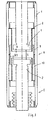
- a vacuum bulb A intended in particular to be integrated with a medium voltage electrical circuit breaker in order to achieve the cut-off of an electric circuit in the event of a fault or during a command of voluntary opening of the electric circuit.
- This vacuum interrupter A comprises, in a manner known per se, a cylindrical envelope E closed by two bottoms inside which are housed two arcing contacts respectively a fixed arcing contact 1 and a movable arcing contact 2.
- movable contact 2 is mechanically connected via an actuating rod to a control device (not shown), said rod being connected to said device by one of its ends and being secured to the movable arcing contact by its opposite end.
- This control device is able to move the aforementioned rod and the movable contact in translation inside the casing between two positions respectively a closed position of the contacts corresponding to a normal operation of the device and an open position. or separation of the contacts after the appearance of a fault in the electrical circuit to be protected or during a command of voluntary opening of the electrical circuit.
- this cylindrical envelope comprises a single ceramic 4 and the bulb comprises three screens 8,9,10 located around the contacts 1,2, the screens 8,9,10 being arranged all inside the bulb. These screens include a half-potential screen 9, or 50% said screen, surrounding the two contacts 1,2. If the contacts 1 and 2 respectively have a voltage of 100% and 0%, the potential of the screen is at 50% in the middle of the two potentials of the contacts.
- these screens also include two so-called partial screens 8, 10 respectively said first screen 8 at 75% and a second screen 10 at 25%.
- these partial screens 8, 10 are interposed between the screen at mid-potential 9 and the contacts 1,2, said partial screens 8,10 being superimposed over part of their length with the screen at mid-potential 9.
- this cylindrical envelope E comprises four cylindrical ceramic portions 4,5,6,7 said first, second, third and fourth arranged end to end.
- the mid-potential screen 9 is fixed between the two central ceramics 5,6, while the two partial screens 8,10, respectively first 8 and second 10, are respectively fixed between the first 4 and second ceramics 5, for the 8, and between the third and fourth ceramics 6,7, for the other 10.
- the first partial screen 8 surrounds the fixed contact 1 while the second partial screen 10 surrounds the movable contact 2.
- the distance between the mid-potential screen 9 and the contacts 1,2 is such that the electric field at the edge of the contacts is directed towards the partial screens 8,10 surrounding said contacts so as to favor priming between contacts and displays 8,10 rather than between contacts.
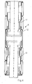
- the bulb according to another embodiment comprises three screens 11,12,13 and four ceramics 4,5,6,7 the mid-potential screen 12 forming part of the envelope of the bulb.
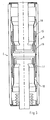
- the bulb according to another embodiment comprises five screens and a single ceramic. It can be seen that two partial screens 14, 15 and 17, 18 are situated between the half-potential screen 16 and each contact 1, 2, the screens 14, 18 partly covering the screens 15, 17.
- the following table shows the distance between the half-potential screen and the contacts_expressed as a function of the contact distance. S is the distance between the contacts.
- the intercalated screen reaches a potential of 100% and the half-potential screen follows this potential change by capacitive coupling and reaches only a potential of 67%.
- the electric field at the end of the contact points towards (or comes from, depending on the polarity of the voltage) the nearest screen that surrounds it.
- the field or end of the screen points (or just, depending on the polarity of the voltage) to the nearest screen around it.
- the screens and the contacts have a capacitance between them such that the potential difference ⁇ U between two surrounding screens or between a contact and the screen surrounding it is almost identical.
- the potential difference ⁇ U must, to be acceptable, be between 15% and 35%, and will advantageously be close to 25% of the total voltage.
- this potential difference ⁇ U does not vary more than 40% with respect to the total U ratio / (N +1), U total being the voltage between the contacts.
- the partial screens 8,10 interspersed exceed the contact they surround with a value H between 0 and S / 3, S being the distance between the contacts and preferably a close height of S / 4.
- the distance SE1 between the half-potential screen 9 and the contact is, to be acceptable, between 25% and 40% of the distance between the contacts S, and preferably equal to 31%.
- ⁇ U deviation of voltage (expressed as a percentage of the total voltage) between two screens that surround each other or between a contact and the screen around it.
- H height of the screens; either in relation to the contact or for two surrounding screens.
- SE1 distance between the contacts and the half-way screen.
- the electric field will be influenced by this approximation and will begin to increase.
- SE the distance between the contact and the screen at 50%
- SE tilting which marks a transition in the direction of the electric field so that for SE> SE (tilting), the field electrical point towards the other contact and that for SE ⁇ SE (tilt) the electric field points towards the screen at 50%.
- SE tilting the distance between the contact and the screen at 50%
- SE tilting the distance between the contact and the screen at 50%
- the figure 2 represents the distance between the contacts and the central screen as a function of the distance between the contacts.
- Curve a represents the distance between the contacts and the screen, recommended by the prior art in particular in the patent DE 10029763 .
- the curve b represents the minimum distance that allows according to the prior art to avoid interaction between the contacts and the screen.
- Curve c represents, in a three-screen configuration according to the invention, the distance between the contacts and the screen which gives an electric field to the edge of the contacts identical to the case of the curve a, and the curve d represents the distance between the contacts and the screen which gives an electric field to the edge of the contacts identical to that of the curve b.
- the distance between the half-potential screen and the contacts is between the curves a and b, while according to the invention, this distance is between the curves c and d.
- a gain of 50 to 70% can be obtained on the distance between the screen and the contacts for a bulb with three screens.
- An additional gain can be obtained with a light bulb according to the invention comprising five screens or seven screens as represented on the figures 4 ,and 5 as shown in the table. Indeed, for a five-screen bulb, the distance between the screen and the contacts is between 0.19 * S and 0.21 * S, where S is the distance between the contacts.
- An even greater gain can be achieved with a cartridge according to the invention having seven screens, for which the distance between the screen and the contact is between 0.14 and 0.16 * S * S.
- the invention is not limited to the given embodiments only. for example.
- the invention covers any embodiment of bulb having an odd number of screens, the potential screens closer to that of the contacts being placed so as to hide over a certain length of the screen at mid-potential. or the other partial screens, in the case where the bulb has more than three screens, with respect to this contact, the electric field at the end of the contact pointing to (or coming from according to the polarity of the voltage) the screen the most surrounding area and the electric field at the end of the partial screen (other than the half-potential screen) pointing to (or coming from, depending on the polarity of the voltage) the nearest partial screen that 'surrounded.
Landscapes
- High-Tension Arc-Extinguishing Switches Without Spraying Means (AREA)
- Vessels And Coating Films For Discharge Lamps (AREA)
Claims (13)
- Vakuumschaltröhre für ein elektrisches Schaltgerät wie zum Beispiel einen Trennschalter, Lastschalter oder Leistungsschalter, welche Schaltröhre ein annähernd zylindrisches und durch zwei Böden verschlossenes Gehäuse, zwei im Inneren des Gehäuses axial angeordnete Kontakte, von denen mindestens einer, der als beweglicher Kontakt bezeichnet wird, mit einem Schaltmechanismus verbunden ist und zwischen einer den Stromfluss ermöglichenden Einschaltstellung der Kontakte und einer Stellung verschoben werden kann, in der die Kontakte voneinander getrennt sind und die zwischen ihnen bestehende Spannung aufrechterhalten, sowie mindestens einen, um mindestens einen der Kontakte geführten leitenden Schirm umfasst, wobei die Vakuumschaltröhre mindestens drei Schirme (8 bis 18) umfasst, zu denen ein zwischen den beiden Kontakten (1, 2) angeordneter, so genannter Halbpotentialschirm (9, 12, 16) sowie ein so genannter erster Teilschirm und ein so genannter zweiter Teilschirm (8, 10, 11, 13, 14, 18) gehören, welche Teilschirme jeweils zwischen dem genannten Halbpotentialschirm (9, 12, 16) und einem der beiden Kontakte (1, 2) angeordnet sind, wobei die genannten Schirme an einem Punkt des Gehäuses ohne elektrische Verbindung zu einem der Kontakte befestigt sind, dadurch gekennzeichnet, dass der Abstand zwischen dem genannten Halbpotentialschirm (9, 12, 16) und den Kontakten (1, 2) zwischen 25 % und 40 % des Abstands zwischen den Kontakten beträgt, derart dass das am Rand des Kontakts (1, 2) vorhandene elektrische Feld vom Kontakt (1, 2) zum Teilschirm (oder in Abhängigkeit von der Polarität der Spannung umgekehrt vom Teilschirm zum Kontakt) gerichtet ist.
- Vakuumschaltröhre nach Anspruch 1, dadurch gekennzeichnet, dass sie drei Schirme (8, 9, 10) bzw. (11, 12, 13) umfasst, dass das Isolierstoffgehäuse vier stoßend aufeinander liegende Keramikabschnitte (4, 5, 6, 7) umfasst und dass die drei Schirme an den drei Stoßstellen zwischen jeweils zwei aneinandergrenzenden Keramikabschnitten angeordnet sind.
- Vakuumschaltröhre nach Anspruch 1 oder 2, dadurch gekennzeichnet, dass der Halbpotentialschirm (9) als Teil des Gehäuses der Schaltröhre ausgebildet ist.
- Vakuumschaltröhre nach irgendeinem der Ansprüche 1 bis 3, dadurch gekennzeichnet, dass der genannte Abstand annähernd 31 % beträgt.
- Vakuumschaltröhre nach irgendeinem der vorhergehenden Ansprüche, dadurch gekennzeichnet, dass die Höhe des Teilschirms bzw. der Teilschirme (8, 10, 11, 13) um ein Maß H zwischen 0 und S/3 größer ist als die Höhe des bzw. der Kontakte (1, 2) oder des bzw. der anderen Teilschirme, die sie umgeben, wobei S dem Abstand zwischen den Kontakten (1, 2) entspricht.
- Vakuumschaltröhre nach Anspruch 5, dadurch gekennzeichnet, dass die Höhe des Teilschirms bzw. der Teilschirme (8, 10, 11, 13) um ein Maß H von etwa S/4 größer ist als die Höhe des Kontakts bzw. der Kontakte (1, 2), um die sie geführt sind.
- Vakuumschaltröhre nach irgendeinem der vorhergehenden Ansprüche, dadurch gekennzeichnet, dass mindestens einer der Schirme zylinderförmig ausgebildet ist.
- Vakuumschaltröhre nach irgendeinem der vorhergehenden Ansprüche, dadurch gekennzeichnet, dass sie mindestens einen weiteren Teilschirm umfasst (14, 18) der zwischen mindestens einem der Kontakte (1, 2) und einem der genannten Teilschirme (15, 17) angeordnet ist, wobei der Abstand zwischen dem Halbpotentialschirm (16) und den Kontakten (1, 2) so gewählt ist, dass das elektrische Feld am Rand der Kontakte (1, 2) zu dem Teilschirm bzw. den Teilschirmen (14, 18) gerichtet ist, welche die Kontakte (1, 2) unmittelbar umgeben.
- Vakuumschaltröhre nach irgendeinem der vorhergehenden Ansprüche, dadurch gekennzeichnet, dass sie zwei Teilschirme, die als erster Teilschirm (15) und zweiter Teilschirm (17) bezeichnet werden und zwischen dem Halbpotentialschirm (16) und den beiden Kontakten (1, 2) angeordnet sind, sowie zwei weitere Teilschirme umfasst, die als dritter Teilschirm (14) und vierter Teilschirm (18) bezeichnet werden und zwischen dem ersten (15) bzw. zweiten Teilschirm (17) einerseits und den beiden Kontakten (1, 2) andererseits angeordnet sind.
- Vakuumschaltröhre nach irgendeinem der vorhergehenden Ansprüche, dadurch gekennzeichnet, dass die relative Kapazität der Schirme und der Kontakte (1, 2) so bemessen ist, dass die Potentialdifferenz δU zwischen den beiden, sich einander umgebenden Schirmen annähernd der Kapazität zwischen einem Kontakt und dem ihn umgebenden Schirm entspricht.
- Vakuumschaltröhre nach irgendeinem der Ansprüche 1 bis 7, dadurch gekennzeichnet, dass die relative Kapazität der Schirme und der Kontakte (1, 2) so bemessen ist, dass die Potentialdifferenz δU zwischen den beiden, sich einander umgebenden Schirmen annähernd der Kapazität zwischen einem Kontakt und dem ihn umgebenden Schirm entspricht, wobei die genannte Potentialdifferenz δU zwischen 15 % und 35 % der Gesamtspannung beträgt.
- Vakuumschaltröhre nach irgendeinem der Ansprüche 1 bis 7, dadurch gekennzeichnet, dass die relative Kapazität der Schirme und der Kontakte (1, 2) so bemessen ist, dass die Potentialdifferenz δU zwischen den beiden, sich einander umgebenden Schirmen annähernd der Kapazität zwischen einem Kontakt und dem ihn umgebenden Schirm entspricht, wobei die genannte Potentialdifferenz δU etwa 25 % der Gesamtspannung beträgt.
- Vakuumschaltröhre nach Anspruch 10 mit N Schirmen, dadurch gekennzeichnet, dass diese Potentialdifferenz δU nicht mehr als 40 % von dem Verhältnis Uges/(N+1) beträgt, wobei Uges der Spannung zwischen den Kontakten entspricht.
Applications Claiming Priority (2)
| Application Number | Priority Date | Filing Date | Title |
|---|---|---|---|
| FR0506550A FR2887683A1 (fr) | 2005-06-28 | 2005-06-28 | Ampoule a vide pour un appareil de protection electrique tel un interrupteur ou un disjoncteur |
| PCT/FR2006/001274 WO2007003727A1 (fr) | 2005-06-28 | 2006-06-06 | Ampoule a vide pour un appareil de protection electrique tel un interrupteur ou un disjoncteur |
Publications (2)
| Publication Number | Publication Date |
|---|---|
| EP1897107A1 EP1897107A1 (de) | 2008-03-12 |
| EP1897107B1 true EP1897107B1 (de) | 2012-04-25 |
Family
ID=35519998
Family Applications (1)
| Application Number | Title | Priority Date | Filing Date |
|---|---|---|---|
| EP06764739A Not-in-force EP1897107B1 (de) | 2005-06-28 | 2006-06-06 | Unterdruck-birne für eine elektrische schutzvorrichtung wie etwa einen schalter oder einen unterbrecherschalter |
Country Status (8)
| Country | Link |
|---|---|
| US (1) | US8445804B2 (de) |
| EP (1) | EP1897107B1 (de) |
| JP (1) | JP5095614B2 (de) |
| CN (2) | CN101208763A (de) |
| AT (1) | ATE555490T1 (de) |
| CA (1) | CA2612730C (de) |
| FR (1) | FR2887683A1 (de) |
| WO (1) | WO2007003727A1 (de) |
Cited By (1)
| Publication number | Priority date | Publication date | Assignee | Title |
|---|---|---|---|---|
| EP3229254B1 (de) | 2016-04-05 | 2018-12-05 | LSIS Co., Ltd. | Vakuumunterbrecher für einen vakuumschutzschalter |
Families Citing this family (12)
| Publication number | Priority date | Publication date | Assignee | Title |
|---|---|---|---|---|
| DE102007004430B4 (de) * | 2007-01-24 | 2009-02-05 | Siemens Ag | Vakuumschalter |
| DE102009031598B4 (de) | 2009-07-06 | 2011-06-01 | Siemens Aktiengesellschaft | Vakuumschaltröhre |
| ES2523279T3 (es) * | 2010-03-01 | 2014-11-24 | Eaton Industries (Netherlands) B.V. | Una disposición de interrupción para un aparellaje eléctrico |
| KR101100708B1 (ko) | 2010-05-13 | 2011-12-30 | 엘에스산전 주식회사 | 진공 차단기 |
| JP5475601B2 (ja) * | 2010-09-15 | 2014-04-16 | 株式会社東芝 | 真空バルブ |
| EP2469561B1 (de) * | 2010-12-23 | 2017-04-05 | ABB Schweiz AG | Vakuumstromunterbrecheranordnung für einen Schutzschalter |
| CN102254734B (zh) * | 2011-06-30 | 2013-10-16 | 西安交通大学 | 高电压单断口真空灭弧室 |
| US10978256B1 (en) | 2013-03-15 | 2021-04-13 | Innovative Switchgear IP, LLC | Electrical switching device |
| DE102016214750A1 (de) * | 2016-05-19 | 2017-11-23 | Siemens Aktiengesellschaft | Verfahren zur Herstellung eines keramischen Isolators |
| JP7028270B2 (ja) * | 2020-03-23 | 2022-03-02 | 株式会社明電舎 | 真空インタラプタおよび真空遮断器 |
| EP4177924B1 (de) * | 2021-11-04 | 2025-12-31 | Abb Schweiz Ag | Vakuumunterbrecheranordnung, schaltanlage mit vakuumunterbrecheranordnung und verfahren zur konfigurierung einer vakuumunterbrecheranordnung |
| US12362115B2 (en) * | 2021-12-02 | 2025-07-15 | Meidensha Corporation | Vacuum interrupter |
Family Cites Families (12)
| Publication number | Priority date | Publication date | Assignee | Title |
|---|---|---|---|---|
| GB1027786A (en) * | 1965-02-03 | 1966-04-27 | Gen Electric | Improvements in vacuum type electric circuit interrupters |
| GB1441479A (en) * | 1973-02-16 | 1976-06-30 | Meidensha Electric Mfg Co Ltd | Vacuum circuit breaker assembly |
| JPS49105969A (de) * | 1973-02-16 | 1974-10-07 | ||
| JPS53146179A (en) * | 1977-05-25 | 1978-12-19 | Tokyo Shibaura Electric Co | Vacuum valve |
| US4215255A (en) * | 1978-01-05 | 1980-07-29 | Electric Power Research Institute, Inc. | Vacuum arc switching device with internal shielding |
| JPS5626271Y2 (de) * | 1978-08-31 | 1981-06-22 | ||
| JPS5582738U (de) * | 1978-12-04 | 1980-06-07 | ||
| JPS5780625A (en) * | 1980-11-06 | 1982-05-20 | Meidensha Electric Mfg Co Ltd | Vacuum breaker |
| CN1016121B (zh) * | 1987-09-29 | 1992-04-01 | 三菱电机株式会社 | 真空放电装置 |
| JP3664899B2 (ja) * | 1998-11-27 | 2005-06-29 | 株式会社東芝 | 真空開閉装置 |
| DE10029763B4 (de) | 2000-06-16 | 2009-01-15 | Siemens Ag | Vakuumschaltröhre |
| CN2442381Y (zh) * | 2000-09-01 | 2001-08-08 | 山东晨鸿电工有限责任公司 | 改进的高压真空灭弧室 |
-
2005
- 2005-06-28 FR FR0506550A patent/FR2887683A1/fr not_active Withdrawn
-
2006
- 2006-06-06 CN CNA2006800229141A patent/CN101208763A/zh active Pending
- 2006-06-06 WO PCT/FR2006/001274 patent/WO2007003727A1/fr not_active Ceased
- 2006-06-06 CN CN201410520294.0A patent/CN104299838A/zh active Pending
- 2006-06-06 US US11/922,046 patent/US8445804B2/en active Active
- 2006-06-06 CA CA2612730A patent/CA2612730C/en active Active
- 2006-06-06 EP EP06764739A patent/EP1897107B1/de not_active Not-in-force
- 2006-06-06 JP JP2008518894A patent/JP5095614B2/ja active Active
- 2006-06-06 AT AT06764739T patent/ATE555490T1/de active
Cited By (1)
| Publication number | Priority date | Publication date | Assignee | Title |
|---|---|---|---|---|
| EP3229254B1 (de) | 2016-04-05 | 2018-12-05 | LSIS Co., Ltd. | Vakuumunterbrecher für einen vakuumschutzschalter |
Also Published As
| Publication number | Publication date |
|---|---|
| CA2612730A1 (en) | 2007-01-11 |
| EP1897107A1 (de) | 2008-03-12 |
| JP2008544470A (ja) | 2008-12-04 |
| CN104299838A (zh) | 2015-01-21 |
| CN101208763A (zh) | 2008-06-25 |
| US8445804B2 (en) | 2013-05-21 |
| CA2612730C (en) | 2014-04-29 |
| FR2887683A1 (fr) | 2006-12-29 |
| WO2007003727A1 (fr) | 2007-01-11 |
| US20090095718A1 (en) | 2009-04-16 |
| ATE555490T1 (de) | 2012-05-15 |
| JP5095614B2 (ja) | 2012-12-12 |
Similar Documents
| Publication | Publication Date | Title |
|---|---|---|
| EP0538157B1 (de) | Hybridschalter mit Axialblasspule | |
| EP1897107B1 (de) | Unterdruck-birne für eine elektrische schutzvorrichtung wie etwa einen schalter oder einen unterbrecherschalter | |
| EP0298809B1 (de) | Selbstbeblasender elektrischer Lastschalter mit rotierendem Lichtbogen | |
| EP0433184A1 (de) | Hybrid-Mittelspannungsschalter | |
| FR2814588A1 (fr) | Interrupteur de circuit possedant une fonction hybride d'extinction d'arc | |
| EP3493235B1 (de) | Vakuumlampe für elektrisches stromunterbrechungsgerät | |
| EP0821382B1 (de) | Hochspannungsschalter mit Selbstbeblasung | |
| EP1376634B1 (de) | Vakuumröhre für elektrisches Schutzgerät wie z.B. einen Schalter oder einen Lastschalter | |
| FR2476381A1 (fr) | Sectionneur isole par gaz | |
| EP3230997B1 (de) | Elektrische hochspannungsschutzschaltervorrichtung mit optimierter automatischer löschung | |
| FR2812771A1 (fr) | Mecanisme de commutateur a isolation par gaz hybride | |
| EP0536039A1 (de) | Ultra-Hochspannungsschalter | |
| EP1507274B1 (de) | Erdungsschalter | |
| EP4343808A1 (de) | Nichtelektrische vorrichtung zum ersetzen eines stromsensors in einer schaltkammer eines lasttrennschalters sowie lasttrennschalter mit einer solchen nicht-elektrischen vorrichtung | |
| EP0794545B1 (de) | Vakuumschalter oder Lastschalter | |
| EP2201588B1 (de) | Kompakter schutzschalter mit gemeinsamer übertragung und zwei ausgerichteten trennkammern | |
| EP3968350B1 (de) | Vakuumlampe für stromunterbrechungsgerät | |
| FR2966972A1 (fr) | Appareillage electrique sous enveloppe metallique comportant au moins un capot pare-effluve assurant des echanges convectifs | |
| EP0236641B1 (de) | Trennschalter einer metallgekapselten Hochspannungsanlage | |
| EP0788125B1 (de) | Hochspannungslastschalter mit Einschalt-Widerstand | |
| FR2678770A1 (fr) | Disjoncteur hybride haute tension a grande tension d'arc. | |
| FR2745118A1 (fr) | Interrupteur ou disjoncteur a vide | |
| EP1170766A1 (de) | Treibstange für einen Hochspannungsschalter | |
| EP2144263B1 (de) | Elektrogeräte unter einer Metallhülle mit reduziertem Spannungsgradienten | |
| FR2681979A1 (fr) | Appareil de commutation electrique. |
Legal Events
| Date | Code | Title | Description |
|---|---|---|---|
| PUAI | Public reference made under article 153(3) epc to a published international application that has entered the european phase |
Free format text: ORIGINAL CODE: 0009012 |
|
| 17P | Request for examination filed |
Effective date: 20071113 |
|
| AK | Designated contracting states |
Kind code of ref document: A1 Designated state(s): AT BE BG CH CY CZ DE DK EE ES FI FR GB GR HU IE IS IT LI LT LU LV MC NL PL PT RO SE SI SK TR |
|
| DAX | Request for extension of the european patent (deleted) | ||
| RIN1 | Information on inventor provided before grant (corrected) |
Inventor name: YVARS, BERNARD Inventor name: OLIVE, SERGE Inventor name: SCHELLEKENS, HANS Inventor name: CARDOLETTI, OLIVIER |
|
| DAX | Request for extension of the european patent (deleted) | ||
| RAP1 | Party data changed (applicant data changed or rights of an application transferred) |
Owner name: SCHNEIDER ELECTRIC INDUSTRIES SAS |
|
| 17Q | First examination report despatched |
Effective date: 20101108 |
|
| GRAP | Despatch of communication of intention to grant a patent |
Free format text: ORIGINAL CODE: EPIDOSNIGR1 |
|
| GRAS | Grant fee paid |
Free format text: ORIGINAL CODE: EPIDOSNIGR3 |
|
| GRAA | (expected) grant |
Free format text: ORIGINAL CODE: 0009210 |
|
| AK | Designated contracting states |
Kind code of ref document: B1 Designated state(s): AT BE BG CH CY CZ DE DK EE ES FI FR GB GR HU IE IS IT LI LT LU LV MC NL PL PT RO SE SI SK TR |
|
| REG | Reference to a national code |
Ref country code: GB Ref legal event code: FG4D Free format text: NOT ENGLISH |
|
| REG | Reference to a national code |
Ref country code: CH Ref legal event code: EP |
|
| REG | Reference to a national code |
Ref country code: AT Ref legal event code: REF Ref document number: 555490 Country of ref document: AT Kind code of ref document: T Effective date: 20120515 |
|
| REG | Reference to a national code |
Ref country code: IE Ref legal event code: FG4D Free format text: LANGUAGE OF EP DOCUMENT: FRENCH |
|
| REG | Reference to a national code |
Ref country code: DE Ref legal event code: R096 Ref document number: 602006029097 Country of ref document: DE Effective date: 20120628 |
|
| REG | Reference to a national code |
Ref country code: NL Ref legal event code: VDEP Effective date: 20120425 |
|
| REG | Reference to a national code |
Ref country code: AT Ref legal event code: MK05 Ref document number: 555490 Country of ref document: AT Kind code of ref document: T Effective date: 20120425 |
|
| LTIE | Lt: invalidation of european patent or patent extension |
Effective date: 20120425 |
|
| PG25 | Lapsed in a contracting state [announced via postgrant information from national office to epo] |
Ref country code: LT Free format text: LAPSE BECAUSE OF FAILURE TO SUBMIT A TRANSLATION OF THE DESCRIPTION OR TO PAY THE FEE WITHIN THE PRESCRIBED TIME-LIMIT Effective date: 20120425 Ref country code: SE Free format text: LAPSE BECAUSE OF FAILURE TO SUBMIT A TRANSLATION OF THE DESCRIPTION OR TO PAY THE FEE WITHIN THE PRESCRIBED TIME-LIMIT Effective date: 20120425 Ref country code: CY Free format text: LAPSE BECAUSE OF FAILURE TO SUBMIT A TRANSLATION OF THE DESCRIPTION OR TO PAY THE FEE WITHIN THE PRESCRIBED TIME-LIMIT Effective date: 20120425 Ref country code: PL Free format text: LAPSE BECAUSE OF FAILURE TO SUBMIT A TRANSLATION OF THE DESCRIPTION OR TO PAY THE FEE WITHIN THE PRESCRIBED TIME-LIMIT Effective date: 20120425 Ref country code: IS Free format text: LAPSE BECAUSE OF FAILURE TO SUBMIT A TRANSLATION OF THE DESCRIPTION OR TO PAY THE FEE WITHIN THE PRESCRIBED TIME-LIMIT Effective date: 20120825 Ref country code: FI Free format text: LAPSE BECAUSE OF FAILURE TO SUBMIT A TRANSLATION OF THE DESCRIPTION OR TO PAY THE FEE WITHIN THE PRESCRIBED TIME-LIMIT Effective date: 20120425 |
|
| PG25 | Lapsed in a contracting state [announced via postgrant information from national office to epo] |
Ref country code: SI Free format text: LAPSE BECAUSE OF FAILURE TO SUBMIT A TRANSLATION OF THE DESCRIPTION OR TO PAY THE FEE WITHIN THE PRESCRIBED TIME-LIMIT Effective date: 20120425 Ref country code: PT Free format text: LAPSE BECAUSE OF FAILURE TO SUBMIT A TRANSLATION OF THE DESCRIPTION OR TO PAY THE FEE WITHIN THE PRESCRIBED TIME-LIMIT Effective date: 20120827 Ref country code: GR Free format text: LAPSE BECAUSE OF FAILURE TO SUBMIT A TRANSLATION OF THE DESCRIPTION OR TO PAY THE FEE WITHIN THE PRESCRIBED TIME-LIMIT Effective date: 20120726 Ref country code: LV Free format text: LAPSE BECAUSE OF FAILURE TO SUBMIT A TRANSLATION OF THE DESCRIPTION OR TO PAY THE FEE WITHIN THE PRESCRIBED TIME-LIMIT Effective date: 20120425 |
|
| BERE | Be: lapsed |
Owner name: SCHNEIDER ELECTRIC INDUSTRIES SAS Effective date: 20120630 |
|
| PG25 | Lapsed in a contracting state [announced via postgrant information from national office to epo] |
Ref country code: MC Free format text: LAPSE BECAUSE OF NON-PAYMENT OF DUE FEES Effective date: 20120630 Ref country code: NL Free format text: LAPSE BECAUSE OF FAILURE TO SUBMIT A TRANSLATION OF THE DESCRIPTION OR TO PAY THE FEE WITHIN THE PRESCRIBED TIME-LIMIT Effective date: 20120425 Ref country code: CZ Free format text: LAPSE BECAUSE OF FAILURE TO SUBMIT A TRANSLATION OF THE DESCRIPTION OR TO PAY THE FEE WITHIN THE PRESCRIBED TIME-LIMIT Effective date: 20120425 Ref country code: AT Free format text: LAPSE BECAUSE OF FAILURE TO SUBMIT A TRANSLATION OF THE DESCRIPTION OR TO PAY THE FEE WITHIN THE PRESCRIBED TIME-LIMIT Effective date: 20120425 Ref country code: RO Free format text: LAPSE BECAUSE OF FAILURE TO SUBMIT A TRANSLATION OF THE DESCRIPTION OR TO PAY THE FEE WITHIN THE PRESCRIBED TIME-LIMIT Effective date: 20120425 Ref country code: EE Free format text: LAPSE BECAUSE OF FAILURE TO SUBMIT A TRANSLATION OF THE DESCRIPTION OR TO PAY THE FEE WITHIN THE PRESCRIBED TIME-LIMIT Effective date: 20120425 Ref country code: SK Free format text: LAPSE BECAUSE OF FAILURE TO SUBMIT A TRANSLATION OF THE DESCRIPTION OR TO PAY THE FEE WITHIN THE PRESCRIBED TIME-LIMIT Effective date: 20120425 Ref country code: DK Free format text: LAPSE BECAUSE OF FAILURE TO SUBMIT A TRANSLATION OF THE DESCRIPTION OR TO PAY THE FEE WITHIN THE PRESCRIBED TIME-LIMIT Effective date: 20120425 |
|
| REG | Reference to a national code |
Ref country code: CH Ref legal event code: PL |
|
| REG | Reference to a national code |
Ref country code: CH Ref legal event code: PL |
|
| PG25 | Lapsed in a contracting state [announced via postgrant information from national office to epo] |
Ref country code: IT Free format text: LAPSE BECAUSE OF FAILURE TO SUBMIT A TRANSLATION OF THE DESCRIPTION OR TO PAY THE FEE WITHIN THE PRESCRIBED TIME-LIMIT Effective date: 20120425 |
|
| PLBE | No opposition filed within time limit |
Free format text: ORIGINAL CODE: 0009261 |
|
| STAA | Information on the status of an ep patent application or granted ep patent |
Free format text: STATUS: NO OPPOSITION FILED WITHIN TIME LIMIT |
|
| REG | Reference to a national code |
Ref country code: IE Ref legal event code: MM4A |
|
| 26N | No opposition filed |
Effective date: 20130128 |
|
| PG25 | Lapsed in a contracting state [announced via postgrant information from national office to epo] |
Ref country code: ES Free format text: LAPSE BECAUSE OF FAILURE TO SUBMIT A TRANSLATION OF THE DESCRIPTION OR TO PAY THE FEE WITHIN THE PRESCRIBED TIME-LIMIT Effective date: 20120805 Ref country code: CH Free format text: LAPSE BECAUSE OF NON-PAYMENT OF DUE FEES Effective date: 20120630 Ref country code: IE Free format text: LAPSE BECAUSE OF NON-PAYMENT OF DUE FEES Effective date: 20120606 Ref country code: BE Free format text: LAPSE BECAUSE OF NON-PAYMENT OF DUE FEES Effective date: 20120630 Ref country code: LI Free format text: LAPSE BECAUSE OF NON-PAYMENT OF DUE FEES Effective date: 20120630 |
|
| REG | Reference to a national code |
Ref country code: DE Ref legal event code: R097 Ref document number: 602006029097 Country of ref document: DE Effective date: 20130128 |
|
| PG25 | Lapsed in a contracting state [announced via postgrant information from national office to epo] |
Ref country code: BG Free format text: LAPSE BECAUSE OF FAILURE TO SUBMIT A TRANSLATION OF THE DESCRIPTION OR TO PAY THE FEE WITHIN THE PRESCRIBED TIME-LIMIT Effective date: 20120725 |
|
| PG25 | Lapsed in a contracting state [announced via postgrant information from national office to epo] |
Ref country code: TR Free format text: LAPSE BECAUSE OF FAILURE TO SUBMIT A TRANSLATION OF THE DESCRIPTION OR TO PAY THE FEE WITHIN THE PRESCRIBED TIME-LIMIT Effective date: 20120425 |
|
| PG25 | Lapsed in a contracting state [announced via postgrant information from national office to epo] |
Ref country code: LU Free format text: LAPSE BECAUSE OF NON-PAYMENT OF DUE FEES Effective date: 20120606 |
|
| PG25 | Lapsed in a contracting state [announced via postgrant information from national office to epo] |
Ref country code: HU Free format text: LAPSE BECAUSE OF FAILURE TO SUBMIT A TRANSLATION OF THE DESCRIPTION OR TO PAY THE FEE WITHIN THE PRESCRIBED TIME-LIMIT Effective date: 20060606 |
|
| REG | Reference to a national code |
Ref country code: FR Ref legal event code: PLFP Year of fee payment: 10 |
|
| REG | Reference to a national code |
Ref country code: FR Ref legal event code: PLFP Year of fee payment: 11 |
|
| REG | Reference to a national code |
Ref country code: FR Ref legal event code: PLFP Year of fee payment: 12 |
|
| REG | Reference to a national code |
Ref country code: FR Ref legal event code: PLFP Year of fee payment: 13 |
|
| PGFP | Annual fee paid to national office [announced via postgrant information from national office to epo] |
Ref country code: GB Payment date: 20240618 Year of fee payment: 19 |
|
| PGFP | Annual fee paid to national office [announced via postgrant information from national office to epo] |
Ref country code: DE Payment date: 20240627 Year of fee payment: 19 |
|
| PGFP | Annual fee paid to national office [announced via postgrant information from national office to epo] |
Ref country code: FR Payment date: 20240625 Year of fee payment: 19 |
|
| REG | Reference to a national code |
Ref country code: DE Ref legal event code: R119 Ref document number: 602006029097 Country of ref document: DE |
|
| GBPC | Gb: european patent ceased through non-payment of renewal fee |
Effective date: 20250606 |
|
| PG25 | Lapsed in a contracting state [announced via postgrant information from national office to epo] |
Ref country code: GB Free format text: LAPSE BECAUSE OF NON-PAYMENT OF DUE FEES Effective date: 20250606 |
|
| PG25 | Lapsed in a contracting state [announced via postgrant information from national office to epo] |
Ref country code: DE Free format text: LAPSE BECAUSE OF NON-PAYMENT OF DUE FEES Effective date: 20260101 |
|
| PG25 | Lapsed in a contracting state [announced via postgrant information from national office to epo] |
Ref country code: FR Free format text: LAPSE BECAUSE OF NON-PAYMENT OF DUE FEES Effective date: 20250630 |