EP1898522A2 - Système amplificateur de puissance et terminal de téléphone mobile l'utilisant - Google Patents
Système amplificateur de puissance et terminal de téléphone mobile l'utilisant Download PDFInfo
- Publication number
- EP1898522A2 EP1898522A2 EP07253384A EP07253384A EP1898522A2 EP 1898522 A2 EP1898522 A2 EP 1898522A2 EP 07253384 A EP07253384 A EP 07253384A EP 07253384 A EP07253384 A EP 07253384A EP 1898522 A2 EP1898522 A2 EP 1898522A2
- Authority
- EP
- European Patent Office
- Prior art keywords
- power amplifier
- output
- harmonic
- adder
- signal
- Prior art date
- Legal status (The legal status is an assumption and is not a legal conclusion. Google has not performed a legal analysis and makes no representation as to the accuracy of the status listed.)
- Granted
Links
Images



Classifications
-
- H—ELECTRICITY
- H03—ELECTRONIC CIRCUITRY
- H03F—AMPLIFIERS
- H03F3/00—Amplifiers with only discharge tubes or only semiconductor devices as amplifying elements
- H03F3/20—Power amplifiers, e.g. Class B amplifiers, Class C amplifiers
-
- H—ELECTRICITY
- H03—ELECTRONIC CIRCUITRY
- H03F—AMPLIFIERS
- H03F1/00—Details of amplifiers with only discharge tubes, only semiconductor devices or only unspecified devices as amplifying elements
- H03F1/32—Modifications of amplifiers to reduce non-linear distortion
- H03F1/3241—Modifications of amplifiers to reduce non-linear distortion using predistortion circuits
- H03F1/3258—Modifications of amplifiers to reduce non-linear distortion using predistortion circuits based on polynomial terms
-
- H—ELECTRICITY
- H03—ELECTRONIC CIRCUITRY
- H03F—AMPLIFIERS
- H03F1/00—Details of amplifiers with only discharge tubes, only semiconductor devices or only unspecified devices as amplifying elements
- H03F1/32—Modifications of amplifiers to reduce non-linear distortion
- H03F1/3241—Modifications of amplifiers to reduce non-linear distortion using predistortion circuits
- H03F1/3276—Modifications of amplifiers to reduce non-linear distortion using predistortion circuits using the nonlinearity inherent to components, e.g. a diode
-
- H—ELECTRICITY
- H03—ELECTRONIC CIRCUITRY
- H03F—AMPLIFIERS
- H03F3/00—Amplifiers with only discharge tubes or only semiconductor devices as amplifying elements
- H03F3/189—High-frequency amplifiers, e.g. radio frequency amplifiers
-
- H—ELECTRICITY
- H03—ELECTRONIC CIRCUITRY
- H03F—AMPLIFIERS
- H03F3/00—Amplifiers with only discharge tubes or only semiconductor devices as amplifying elements
- H03F3/68—Combinations of amplifiers, e.g. multi-channel amplifiers for stereophonics
-
- H—ELECTRICITY
- H04—ELECTRIC COMMUNICATION TECHNIQUE
- H04B—TRANSMISSION
- H04B1/00—Details of transmission systems, not covered by a single one of groups H04B3/00 - H04B13/00; Details of transmission systems not characterised by the medium used for transmission
- H04B1/02—Transmitters
- H04B1/04—Circuits
- H04B1/0475—Circuits with means for limiting noise, interference or distortion
Definitions
- the present invention relates to a power amplifier system and a mobile phone terminal using the same.
- HSDPA high speed down Link packet access
- DPCCH dedicated packet control channel
- a first related art example is a "digital cross-cancellation (or "DCC") system," such as described in Patent Publication 1 ( Japanese Patent Application Publication No. 2005-45767 ) will be described here.
- DCC digital cross-cancellation
- a digital signal processor or "DSP”
- DSP digital signal processor
- desired compactness cannot be achieved, and power consumption is significantly large because of the DSP being used.
- a second related art example is a "multistage Doherty amplifier," such as described in Patent Publication 2 (PCT Patent Publication No. 2003-536313 ).
- PCT Patent Publication No. 2003-536313 Patent Publication No. 2003-536313
- a large number of power amplifiers are used for drive amplifiers, and signal distortion generated by the respective power amplifier is minimized, thereby to implement distortion reduction.
- problems arise in that it is difficult to set a minimum distortion point of the respective amplifier, further, a distortion component contained in a final output is cannot be reduced lower than a distortion component generated in the respective amplifier.
- a third related art example is a "microwave Doherty amplifier," such as described in Patent Publication 3 ( Japanese Patent Application Publication No. 1995-22952 ).
- a second harmonic short circuit is combined with a Doherty amplifier, thereby to implementing high efficiency and distortion reduction.
- a distortion reduction effect of the technique using the second harmonic short circuit is, at most, 3 dB, which is insufficient as described in Non-Patent Publication 1 (see (*1) below) (*1): S. Kusunoki, et al., "Harmonic-Injected Power Amplifier with 2nd Harmonic Short Circuit for Cellular Phones", IEICE Transaction on Electronics vol. E88-C, No. 4, April 2005, pp. 729-738
- the feature of the signal of high peak factor is the high peak power.
- a power amplifier for use is desired to be capable of implementing high saturation output and low distortion.
- Candidates of such an amplifier include a Doherty amplifier.
- the amplifier is capable of implementing high saturation output and high efficiency.
- the Doherty amplifier is less advantageous in terms of distortion reduction as it uses class C amplifiers.
- a power amplifier system includes a first power amplifier for amplifying a primary input signal; a second harmonic generator for outputting a second harmonic by using a split part (split signal) of the primary input signal as an input; a phase shifter for adjusting a phase of the second harmonic; a first adder for summing together the split signal of the primary input signal and an output of the phase shifter, thereby to produce an output; a second power amplifier that uses the output of the first adder as an input; and a second adder for summing together an output of the first amplifier and an output of the second power amplifier, thereby to produce an output.
- the outputs of the first and second power amplifiers may be summed together and combined thereby. According to the combination of the first and second power amplifiers, a high saturation output and a high efficiency can be obtained.
- the second harmonic generator may use the split part of the primary input signal as the input, and thereby outputs a second harmonic.
- the phase shifter may adjust the phase of the second harmonic.
- An output of the phase shifter may be output after being summed by the first adder to a split signal of the primary input signal.
- the output of the first adder may be input to the second power amplifier.
- a high saturation output can be produced by combining the two power amplifiers, signal distortion can be greatly reduced in the manner that distortion signals are cross-cancelled by reverse phases.
- the invention preferably also relates to an HF (high frequency) power amplifier system usable with a mobile phone terminal and an HF power frequency power amplifier system usable with a mobile phone terminal, and a mobile phone using the HF power amplifier system.
- HF high frequency
- FIG. 1 is a block diagram of a general configuration of a power amplifier system of one embodiment of the present invention.
- the power amplifier system includes a first power amplifier 40 ("PA_1 "), a second harmonic generator 10 ("2nd_gen"), a phase shifter 20 ("ph”), a first adder 30 ("add1 "), a second power amplifier 50 (“PA_2”), and a second adder 60 (“add2”).
- the first power amplifier 40 (“PA_1”) amplifies a primary input signal (“sigin”)
- the second harmonic generator 10 splits the input signal (“sigin”), inputs a split part (signal), and then outputs a second harmonic.
- the phase shifter 20 adjusts the phase of the second harmonic.
- the first adder 30 (“add1") performs addition or summation of the split signal of the primary input signal (“sigin”) and the output of the phase shifter 20, and produces an output as a result of the summation.
- the second power amplifier 50 inputs the output of the first adder 30 ("add1") for amplification.
- the second adder 60 (“add2") performs summation of the respective outputs of the power amplifiers 40 and 50, and in turn outputs an output signal (“sigout”) as a result of the summation.
- the power amplifier 40 is biased to the A or AB class, and the power amplifier 50 is biased to the class C.
- a power value of the input signal (“sigin") is low (in comparison to a predetermined value)
- the power amplifier 40 enters an active mode, and the power amplifier 50 enters a pause mode.
- the power amplifier 50 enters the active mode, and two outputs are summed together. In this event, the respective phases passing through the power amplifiers 40 and 50 are adjusted to the same value, whereby the outputs of the respective power amplifiers 40 and 50 are combined in the same phase.
- the power amplifier 40, 50 produces the output containing nonlinear distortion.
- IM3 third order intermodulation distortion
- a general two-tone signal (frequency w1, w1 + ⁇ ) represents the primary input signal ("sigin").
- H3 is a third order nonlinear transfer function of the power amplifier
- an IM3 component can be represented as: H3 ⁇ exp(j ⁇ (w1 + 2 ⁇ + ⁇ )). In this case, ⁇ is the phase.
- the (w1 - ⁇ ) components are not taken into account for the sake of simplicity of description.
- IM3 occurs in a similar manner from each of the two power amplifiers 40 and 50, and is summed by the second adder 60 ("add2").
- the second adder 60 (“add2") is operated so that the respective components (signal components) of the frequencies W1 and W2 are summed together in the same phase, that is, the output of the signal components is maximized.
- the summation of IM3 components contained in the outputs of the respective power amplifiers is determined by the phases ⁇ of the respective IM3 components. If the phases ⁇ of the IM3 components can be set to be mutually reverse phases while the phases of the signal components are being carried, respective IM3 components contained in the output of the second adder 60 ("add2") are greatly cross-cancelled and hence reduced.
- the above described is implemented in the manner that the second harmonic of the input signal (“sigin”) is input into the second power amplifier 50.
- FIG. 2 is a detailed circuit configuration of the power amplifier system shown in FIG. 1.
- portions corresponding to those shown in FIG. 1 are shown with the same reference characters.
- a FET 12 FET: field effect transistor
- a gate bias voltage vg is applied via a resistor 13 ("r1 ") to the gate terminal of the FET 12.
- a part of the input signal (“sigin") is split by a capacitor 14 ("c1 ") and is input.
- a drain voltage vd is applied to the drain terminal of the FET 12 via a coil 11.
- a second harmonic bandpass filter 15 (“bpf') is coupled to the drain terminal of the FET 12.
- a frequency conversion mixer can be used in lieu of the bandpass filter 15 (“bpf"). In this case, the bandpass filter 15 (“bpf”) is unnecessary.
- the phase shifter 20 for adjusting the phase of the second harmonic is configured using an L-shaped connection circuit including a coil 21 and a capacitor 22. Thereby, only the second harmonic occurring in the Class C amplifier is extracted or drawn, and is into the subsequent second power amplifier 50.
- the first adder 30 (“add1 ”) is configured from a series circuit including a coil 31 and a capacitor 32.
- the first power amplifier 40 has a configuration in which a plurality of FETs, namely an input FET 43 and an output FET 46, which are both of the source-grounded type, are connected.
- a matching circuit 41 is coupled to the gate of the input FET 43, in which the input FET 43 receives the input signal ("sigin") through the matching circuit 41.
- a coil 42 is coupled to the drain terminal of the input FET 43, in which a drain voltage Vdd is applied through the coil 42.
- a matching circuit 44 through which the drain terminal of the input FET 43 is connected to the gate terminal of the output FET 46.
- the drain voltage Vdd is applied to the drain terminal of the output FET 46 via a coil 45.
- the drain terminal of the output FET 46 is connected to one of input ends of the second adder 60 ("add2") via a matching circuit 49 for inputting the drain voltage Vdd thereto.
- the matching circuit 49 is configured from an L-shaped connection circuit including a coil 47 and a capacitor 48.
- the second power amplifier 50 has a configuration similar to that of the first power amplifier 40. More specifically, a plurality of FETs, namely an input FET 53 and an output FET 56, which are both of the source-grounded type, are connected.
- a matching circuit 51 is coupled to the gate of the input FET 53, in which the input FET 53 receives the input signal from the first adder 30 through the matching circuit 51.
- a coil 52 is coupled to the drain terminal of the input FET 53, in which a drain voltage Vdd is applied through the coil 52.
- a matching circuit 54 through which the drain terminal of the input FET 53 is connected to the gate terminal of the output FET 56. The drain voltage Vdd is applied to the drain terminal of the output FET 56 via a coil 55.
- the drain terminal of the output FET 56 is connected to the other input end of the second adder 60 ("add2") via a matching circuit 59 for inputting the drain voltage Vdd thereto.
- the matching circuit 59 is configured from an L-shaped connection circuit including a coil 57 and a capacitor 58.
- the second adder 60 (“add2”) includes two coils 61 and 62 series connected to, in which a summation output (“sigout”) is drawn from a connection point or node between the coils 61 and 62.
- FIG. 3 is a graph showing dependency of the phase (the above-described phase ⁇ ) of IM3 contained in the output of the second power amplifier 50 of FIG. 2 upon the phase of a second harmonic for injection ("injection second harmonic," hereinbelow). It can be known from the graph that IM3 changes about 80 degrees with respect to a 360-degree phase change of the injection second harmonic.
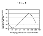
- FIG. 4 is a graph showing variations in the output phase of signal components in the same state as that in FIG. 3. According to the graph, only about 4 degrees is changed with respect to the 360-degree phase change of the injection second harmonic. In other words, it can be known that only the phase of IM3 can be controlled without influencing the phase variations in the signal component. Thereby, the phase can be adjusted to the phase of the second harmonic capable of canceling IM3.
- FIG. 5 is a graph showing input/output characteristics obtained in the circuit configuration of FIG. 2.
- the graph shows the characteristics of signal component outputs 61 and 62 with and without second harmonic injection, a third order intermodulation distortion (IM3) 64 without second harmonic injection, injection second harmonic 63 with second harmonic injection, and a third order intermodulation distortion (IM3) 65 with second harmonic injection corresponding to the level of primary input power.
- the data of the component outputs 61 and 62 substantially overlap one another (the solid line and the broken line) regardless of the second harmonic injection. As such, it can be said that no influence of the second harmonic injection is imposed. This is attributed to the fact that, as shown in FIG. 5, the phase variation due to the second harmonic injection is very small.
- FIG. 5 shows also the level of the second harmonic injection.
- the level of the second harmonic is adjusted at one arbitrary input point, no adjustment has to be done thereafter.
- the level of the second harmonic is increased substantially at a ratio of a tilt "2" ("2" representing the tilt, for example) with respect to an input (that is, at the ratio of a 2-dBm increase with respect to a 1-dBm increase).
- the operation is thus performed so that respective IM3 components similarly occurring from the two power amplifiers 40 and 50 are greatly cross-cancelled.
- the operation will be further described herebelow by using mathematical expressions.
- An input/output characteristic under voltages of the respective power amplifiers is assumed to be as represented by expression (1) below.
- Vo G ⁇ 1 ⁇ Vi + G ⁇ 2 ⁇ Vi 2 + G ⁇ 3 ⁇ Vi 3 + ...
- an input signal into a first power amplifier (lower PA,” hereinbelow) can be represented by expression (2) below.
- Vi sin ⁇ t + sin ⁇ + ⁇ ⁇ t
- the respective amplitude is assumed to be 1 for convenience.
- a phase ⁇ of the respective wave is assumed to be 0.
- IM3L a third order cross modulation distortion component IM3L of the lower PA can be represented by expression (3) below.
- IM ⁇ 3 ⁇ L 3 ⁇ sin ⁇ t ⁇ sin 2 ⁇ ⁇ + ⁇ ⁇ t ⁇ 3 / 2 ⁇ G ⁇ 3 ⁇ sin ⁇ + 2 ⁇ ⁇ ⁇ t
- the input/output characteristic also is assumed to be the same as expression (1) above.
- the output of the upper PA can be obtained by assignment of the expression (4) to expression (1).
- the parameter "-cos( ⁇ +2 ⁇ )t” occurs from the parameter "sin( ⁇ t)-sin ⁇ 2( ⁇ + ⁇ )t ⁇ ” occurring in the second parameter (parameter of G2.
- a third order cross modulation distortion component IM3U can be represented as expression (5) below.
- IM ⁇ 3 ⁇ U sin ⁇ t ⁇ sin ⁇ 2 ⁇ ⁇ + ⁇ ⁇ t - G ⁇ 2 ⁇ cos ⁇ + 2 ⁇ ⁇ ⁇ t
- IM3 components for the combined output of the upper and lower PAs are represented as expressions (6) and (7) below.
- IM ⁇ 3 ⁇ L 3 / 2 ⁇ G ⁇ 3 ⁇ V ⁇ 1 ⁇ sin ⁇ + 2 ⁇ ⁇ ⁇ t + ⁇ ⁇ 1
- IM ⁇ 3 ⁇ U - G ⁇ 2 ⁇ V ⁇ 2 ⁇ cos ⁇ + 2 ⁇ ⁇ ⁇ t + ⁇ ⁇ 2
- the phases ⁇ are significant only for the relative relation between the respective waves.
- the coefficients G of expression (1) representing the input/output characteristics of the amplifiers PA are all complex numbers in practical applications. Further, since the phases have to be taken into account for applying expressions (2) and (4) representing the input signals, the operation becomes even more complex. In particular, specific attention should be paid when handling the phases of the signals. When the frequencies involved or being handled are the same, simple summation (or addition) and subtraction of the phase relations can be performed. However, when, as in the present embodiment, the frequency conversion is involved, the phases of the coefficients G are additionally involved. As such, for implementing a more precise approach, it is preferable that, as described in Non-Patent Publication 1, a method employing the complex Fourier transform be used.
- the power amplifier system of the present embodiment is well suited for adaptation to a mobile phone terminal.
- the terminal includes, for example, a transmit portion, a receive portion, a data processing portion, an operation portion, a display portion, and an audio processing portion.
- the power amplifier system of the present embodiment is used in the transmit portion.
Landscapes
- Engineering & Computer Science (AREA)
- Power Engineering (AREA)
- Physics & Mathematics (AREA)
- Nonlinear Science (AREA)
- Computer Networks & Wireless Communication (AREA)
- Signal Processing (AREA)
- Algebra (AREA)
- General Physics & Mathematics (AREA)
- Mathematical Analysis (AREA)
- Mathematical Optimization (AREA)
- Pure & Applied Mathematics (AREA)
- Amplifiers (AREA)
Applications Claiming Priority (1)
| Application Number | Priority Date | Filing Date | Title |
|---|---|---|---|
| JP2006238113A JP4753255B2 (ja) | 2006-09-01 | 2006-09-01 | 電力増幅装置および携帯電話端末 |
Publications (3)
| Publication Number | Publication Date |
|---|---|
| EP1898522A2 true EP1898522A2 (fr) | 2008-03-12 |
| EP1898522A3 EP1898522A3 (fr) | 2009-04-01 |
| EP1898522B1 EP1898522B1 (fr) | 2010-11-17 |
Family
ID=38739360
Family Applications (1)
| Application Number | Title | Priority Date | Filing Date |
|---|---|---|---|
| EP07253384A Not-in-force EP1898522B1 (fr) | 2006-09-01 | 2007-08-28 | Système amplificateur de puissance et terminal de téléphone mobile l'utilisant |
Country Status (5)
| Country | Link |
|---|---|
| US (1) | US7974597B2 (fr) |
| EP (1) | EP1898522B1 (fr) |
| JP (1) | JP4753255B2 (fr) |
| KR (1) | KR20080020943A (fr) |
| DE (1) | DE602007010557D1 (fr) |
Cited By (1)
| Publication number | Priority date | Publication date | Assignee | Title |
|---|---|---|---|---|
| WO2023180636A1 (fr) * | 2022-03-25 | 2023-09-28 | Institut Polytechnique De Bordeaux | Antenne réseau à commande de phase |
Families Citing this family (6)
| Publication number | Priority date | Publication date | Assignee | Title |
|---|---|---|---|---|
| JP5472119B2 (ja) | 2008-12-25 | 2014-04-16 | 日本電気株式会社 | 電力増幅装置 |
| KR101107628B1 (ko) * | 2010-09-14 | 2012-01-25 | 이형석 | 소송 비용 임치 및 보증을 위한 장치 및 그 방법 및 그 방법을 구현하기 위한 프로그램이 기록된 기록매체 |
| KR101952875B1 (ko) * | 2017-08-24 | 2019-05-23 | 삼성전기주식회사 | 전력 증폭기 및 이를 포함하는 집적회로 |
| CN111615787B (zh) | 2018-01-23 | 2023-08-11 | 株式会社村田制作所 | 功率放大电路 |
| CN111615788B (zh) | 2018-01-23 | 2023-08-01 | 株式会社村田制作所 | 功率放大电路 |
| US11277099B2 (en) * | 2020-06-10 | 2022-03-15 | Nxp Usa, Inc. | Symmetric Doherty amplifier with in-package combining node |
Family Cites Families (14)
| Publication number | Priority date | Publication date | Assignee | Title |
|---|---|---|---|---|
| JP2973684B2 (ja) * | 1992-01-29 | 1999-11-08 | 日本電気株式会社 | 低三次歪み増幅装置 |
| JP3226660B2 (ja) | 1993-05-11 | 2001-11-05 | 旭化成マイクロシステム株式会社 | ディジタルδς変調器 |
| EP0827649A1 (fr) * | 1996-03-20 | 1998-03-11 | Koninklijke Philips Electronics N.V. | Circuit de preaccentuation pour signal analogique dans un reseau de videocommunication |
| SE516145C2 (sv) | 2000-06-06 | 2001-11-26 | Ericsson Telefon Ab L M | Sammansatt förstärkare |
| SE520760C2 (sv) | 2000-06-06 | 2003-08-19 | Ericsson Telefon Ab L M | Doherty-förstärkare av flerstegstyp |
| US6810241B1 (en) * | 2002-01-30 | 2004-10-26 | Northrop Grumman Corporation | Microwave diode mixer |
| JP4209652B2 (ja) * | 2002-09-24 | 2009-01-14 | 三菱電機株式会社 | 高周波電力増幅器 |
| US7129778B2 (en) | 2003-07-23 | 2006-10-31 | Northrop Grumman Corporation | Digital cross cancellation system |
| JP4868433B2 (ja) | 2004-02-09 | 2012-02-01 | ソニー・エリクソン・モバイルコミュニケーションズ株式会社 | 歪み補償装置および歪み補償機能付き電力増幅装置 |
| JP4520204B2 (ja) * | 2004-04-14 | 2010-08-04 | 三菱電機株式会社 | 高周波電力増幅器 |
| JP4671622B2 (ja) * | 2004-04-30 | 2011-04-20 | ソニー・エリクソン・モバイルコミュニケーションズ株式会社 | 歪み補償電力増幅装置 |
| EP1758242A4 (fr) * | 2004-06-18 | 2008-04-09 | Mitsubishi Electric Corp | Amplificateur à haut rendement |
| EP1763921B1 (fr) * | 2004-06-29 | 2012-02-01 | Nxp B.V. | Mecanisme amplificateur du type doherty integre a rendement energetique eleve |
| KR100814415B1 (ko) * | 2007-02-14 | 2008-03-18 | 포항공과대학교 산학협력단 | 하모닉 제어 회로를 이용한 고효율 도허티 전력 증폭기 |
-
2006
- 2006-09-01 JP JP2006238113A patent/JP4753255B2/ja not_active Expired - Fee Related
-
2007
- 2007-08-21 KR KR1020070083867A patent/KR20080020943A/ko not_active Withdrawn
- 2007-08-27 US US11/892,724 patent/US7974597B2/en not_active Expired - Fee Related
- 2007-08-28 EP EP07253384A patent/EP1898522B1/fr not_active Not-in-force
- 2007-08-28 DE DE602007010557T patent/DE602007010557D1/de active Active
Cited By (1)
| Publication number | Priority date | Publication date | Assignee | Title |
|---|---|---|---|---|
| WO2023180636A1 (fr) * | 2022-03-25 | 2023-09-28 | Institut Polytechnique De Bordeaux | Antenne réseau à commande de phase |
Also Published As
| Publication number | Publication date |
|---|---|
| KR20080020943A (ko) | 2008-03-06 |
| JP4753255B2 (ja) | 2011-08-24 |
| US7974597B2 (en) | 2011-07-05 |
| EP1898522B1 (fr) | 2010-11-17 |
| JP2008061123A (ja) | 2008-03-13 |
| DE602007010557D1 (de) | 2010-12-30 |
| US20080058001A1 (en) | 2008-03-06 |
| EP1898522A3 (fr) | 2009-04-01 |
Similar Documents
| Publication | Publication Date | Title |
|---|---|---|
| CN1601892B (zh) | 带预畸变方式畸变补偿功能的放大器 | |
| EP1898522B1 (fr) | Système amplificateur de puissance et terminal de téléphone mobile l'utilisant | |
| US6943628B2 (en) | Methods and apparatus for substantially reducing nonlinear distortion | |
| US7679439B2 (en) | Predistorter | |
| JP4868433B2 (ja) | 歪み補償装置および歪み補償機能付き電力増幅装置 | |
| US6900693B2 (en) | Power amplifying apparatus and radio communications apparatus using same | |
| EP1912328A1 (fr) | Amplificateur hautement efficace | |
| US7307473B2 (en) | Distortion compensating and power amplifying apparatus | |
| JP2002330032A (ja) | 歪み改善回路 | |
| JP2002368547A (ja) | 歪み改善回路 | |
| US20040210789A1 (en) | Distortion compensation circuit, and a transmission apparatus including the same | |
| JP2007215248A (ja) | 電力増幅装置およびこれを用いた無線通信装置 | |
| JP5049562B2 (ja) | 電力増幅器 | |
| JP2008022513A (ja) | 歪制御機能付き増幅装置 | |
| JP4697778B2 (ja) | 歪み補償装置及び歪み補償方法 | |
| JP2001203541A (ja) | 歪補償装置及び歪補償方法、増幅装置並びに無線送信装置 | |
| JP2008258704A (ja) | 増幅装置 | |
| KR20000035036A (ko) | 베이스밴드 신호 처리 회로 | |
| EP2748924B1 (fr) | Circuit et procédé d'amplification de puissance radiofréquence | |
| KR100538267B1 (ko) | 아날로그 제어기를 이용한 적응형 피드포워드선형전력증폭기 및 그 선형화 방법 | |
| JP3495283B2 (ja) | フィードフォワード型増幅器及びこれを用いた無線通信装置 | |
| JPH06252658A (ja) | 広帯域低歪増幅器 | |
| JPH11215197A (ja) | プリディストーション歪補償機能付送信装置及び送信装置におけるプリディストーション歪補償方法 | |
| JP2007312231A (ja) | 帰還増幅装置及びそれを用いた無線回路装置 |
Legal Events
| Date | Code | Title | Description |
|---|---|---|---|
| PUAI | Public reference made under article 153(3) epc to a published international application that has entered the european phase |
Free format text: ORIGINAL CODE: 0009012 |
|
| AK | Designated contracting states |
Kind code of ref document: A2 Designated state(s): AT BE BG CH CY CZ DE DK EE ES FI FR GB GR HU IE IS IT LI LT LU LV MC MT NL PL PT RO SE SI SK TR |
|
| AX | Request for extension of the european patent |
Extension state: AL BA HR MK YU |
|
| PUAL | Search report despatched |
Free format text: ORIGINAL CODE: 0009013 |
|
| AK | Designated contracting states |
Kind code of ref document: A3 Designated state(s): AT BE BG CH CY CZ DE DK EE ES FI FR GB GR HU IE IS IT LI LT LU LV MC MT NL PL PT RO SE SI SK TR |
|
| AX | Request for extension of the european patent |
Extension state: AL BA HR MK RS |
|
| 17P | Request for examination filed |
Effective date: 20090319 |
|
| 17Q | First examination report despatched |
Effective date: 20090512 |
|
| AKX | Designation fees paid |
Designated state(s): DE FR GB |
|
| GRAP | Despatch of communication of intention to grant a patent |
Free format text: ORIGINAL CODE: EPIDOSNIGR1 |
|
| GRAS | Grant fee paid |
Free format text: ORIGINAL CODE: EPIDOSNIGR3 |
|
| GRAA | (expected) grant |
Free format text: ORIGINAL CODE: 0009210 |
|
| AK | Designated contracting states |
Kind code of ref document: B1 Designated state(s): DE FR GB |
|
| REG | Reference to a national code |
Ref country code: GB Ref legal event code: FG4D |
|
| REF | Corresponds to: |
Ref document number: 602007010557 Country of ref document: DE Date of ref document: 20101230 Kind code of ref document: P |
|
| PLBE | No opposition filed within time limit |
Free format text: ORIGINAL CODE: 0009261 |
|
| STAA | Information on the status of an ep patent application or granted ep patent |
Free format text: STATUS: NO OPPOSITION FILED WITHIN TIME LIMIT |
|
| 26N | No opposition filed |
Effective date: 20110818 |
|
| REG | Reference to a national code |
Ref country code: DE Ref legal event code: R097 Ref document number: 602007010557 Country of ref document: DE Effective date: 20110818 |
|
| PGFP | Annual fee paid to national office [announced via postgrant information from national office to epo] |
Ref country code: GB Payment date: 20120821 Year of fee payment: 6 |
|
| PGFP | Annual fee paid to national office [announced via postgrant information from national office to epo] |
Ref country code: FR Payment date: 20120906 Year of fee payment: 6 |
|
| GBPC | Gb: european patent ceased through non-payment of renewal fee |
Effective date: 20130828 |
|
| REG | Reference to a national code |
Ref country code: FR Ref legal event code: ST Effective date: 20140430 |
|
| PG25 | Lapsed in a contracting state [announced via postgrant information from national office to epo] |
Ref country code: GB Free format text: LAPSE BECAUSE OF NON-PAYMENT OF DUE FEES Effective date: 20130828 |
|
| PG25 | Lapsed in a contracting state [announced via postgrant information from national office to epo] |
Ref country code: FR Free format text: LAPSE BECAUSE OF NON-PAYMENT OF DUE FEES Effective date: 20130902 |
|
| REG | Reference to a national code |
Ref country code: DE Ref legal event code: R082 Ref document number: 602007010557 Country of ref document: DE Representative=s name: FDST PATENTANWAELTE FREIER DOERR STAMMLER TSCH, DE Ref country code: DE Ref legal event code: R081 Ref document number: 602007010557 Country of ref document: DE Owner name: SNAPTRACK, INC., SAN DIEGO, US Free format text: FORMER OWNER: SONY ERICSSON MOBILE COMMUNICATIONS JAPAN, INC., TOKIO/TOKYO, JP Ref country code: DE Ref legal event code: R081 Ref document number: 602007010557 Country of ref document: DE Owner name: SONY MOBILE COMMUNICATIONS INC., JP Free format text: FORMER OWNER: SONY ERICSSON MOBILE COMMUNICATIONS JAPAN, INC., TOKIO/TOKYO, JP |
|
| REG | Reference to a national code |
Ref country code: DE Ref legal event code: R082 Ref document number: 602007010557 Country of ref document: DE Representative=s name: FDST PATENTANWAELTE FREIER DOERR STAMMLER TSCH, DE |
|
| REG | Reference to a national code |
Ref country code: FR Ref legal event code: CD Owner name: SNAPTRACK, INC., US Effective date: 20161019 |
|
| REG | Reference to a national code |
Ref country code: FR Ref legal event code: TP Owner name: SNAPTRACK, INC., US Effective date: 20161103 |
|
| REG | Reference to a national code |
Ref country code: DE Ref legal event code: R081 Ref document number: 602007010557 Country of ref document: DE Owner name: SNAPTRACK, INC., SAN DIEGO, US Free format text: FORMER OWNER: SONY MOBILE COMMUNICATIONS INC., TOKYO, JP |
|
| REG | Reference to a national code |
Ref country code: GB Ref legal event code: 732E Free format text: REGISTERED BETWEEN 20170112 AND 20170118 |
|
| REG | Reference to a national code |
Ref country code: DE Ref legal event code: R082 Ref document number: 602007010557 Country of ref document: DE |
|
| PGFP | Annual fee paid to national office [announced via postgrant information from national office to epo] |
Ref country code: DE Payment date: 20170825 Year of fee payment: 11 |
|
| REG | Reference to a national code |
Ref country code: DE Ref legal event code: R119 Ref document number: 602007010557 Country of ref document: DE |
|
| PG25 | Lapsed in a contracting state [announced via postgrant information from national office to epo] |
Ref country code: DE Free format text: LAPSE BECAUSE OF NON-PAYMENT OF DUE FEES Effective date: 20190301 |