EP1900681B1 - Transistors à effet de champ et effet tunnel à base de nanofils de silicium - Google Patents
Transistors à effet de champ et effet tunnel à base de nanofils de silicium Download PDFInfo
- Publication number
- EP1900681B1 EP1900681B1 EP06024507.3A EP06024507A EP1900681B1 EP 1900681 B1 EP1900681 B1 EP 1900681B1 EP 06024507 A EP06024507 A EP 06024507A EP 1900681 B1 EP1900681 B1 EP 1900681B1
- Authority
- EP
- European Patent Office
- Prior art keywords
- tfet
- nanowire
- field effect
- effect transistor
- tunnel field
- Prior art date
- Legal status (The legal status is an assumption and is not a legal conclusion. Google has not performed a legal analysis and makes no representation as to the accuracy of the status listed.)
- Not-in-force
Links
Images




Classifications
-
- H—ELECTRICITY
- H10—SEMICONDUCTOR DEVICES; ELECTRIC SOLID-STATE DEVICES NOT OTHERWISE PROVIDED FOR
- H10D—INORGANIC ELECTRIC SEMICONDUCTOR DEVICES
- H10D62/00—Semiconductor bodies, or regions thereof, of devices having potential barriers
- H10D62/10—Shapes, relative sizes or dispositions of the regions of the semiconductor bodies; Shapes of the semiconductor bodies
- H10D62/117—Shapes of semiconductor bodies
- H10D62/118—Nanostructure semiconductor bodies
-
- B—PERFORMING OPERATIONS; TRANSPORTING
- B82—NANOTECHNOLOGY
- B82Y—SPECIFIC USES OR APPLICATIONS OF NANOSTRUCTURES; MEASUREMENT OR ANALYSIS OF NANOSTRUCTURES; MANUFACTURE OR TREATMENT OF NANOSTRUCTURES
- B82Y10/00—Nanotechnology for information processing, storage or transmission, e.g. quantum computing or single electron logic
-
- H—ELECTRICITY
- H10—SEMICONDUCTOR DEVICES; ELECTRIC SOLID-STATE DEVICES NOT OTHERWISE PROVIDED FOR
- H10D—INORGANIC ELECTRIC SEMICONDUCTOR DEVICES
- H10D12/00—Bipolar devices controlled by the field effect, e.g. insulated-gate bipolar transistors [IGBT]
- H10D12/211—Gated diodes
-
- H—ELECTRICITY
- H10—SEMICONDUCTOR DEVICES; ELECTRIC SOLID-STATE DEVICES NOT OTHERWISE PROVIDED FOR
- H10D—INORGANIC ELECTRIC SEMICONDUCTOR DEVICES
- H10D62/00—Semiconductor bodies, or regions thereof, of devices having potential barriers
- H10D62/10—Shapes, relative sizes or dispositions of the regions of the semiconductor bodies; Shapes of the semiconductor bodies
- H10D62/117—Shapes of semiconductor bodies
- H10D62/118—Nanostructure semiconductor bodies
- H10D62/119—Nanowire, nanosheet or nanotube semiconductor bodies
- H10D62/121—Nanowire, nanosheet or nanotube semiconductor bodies oriented parallel to substrates
-
- H—ELECTRICITY
- H10—SEMICONDUCTOR DEVICES; ELECTRIC SOLID-STATE DEVICES NOT OTHERWISE PROVIDED FOR
- H10D—INORGANIC ELECTRIC SEMICONDUCTOR DEVICES
- H10D62/00—Semiconductor bodies, or regions thereof, of devices having potential barriers
- H10D62/10—Shapes, relative sizes or dispositions of the regions of the semiconductor bodies; Shapes of the semiconductor bodies
- H10D62/117—Shapes of semiconductor bodies
- H10D62/118—Nanostructure semiconductor bodies
- H10D62/119—Nanowire, nanosheet or nanotube semiconductor bodies
- H10D62/122—Nanowire, nanosheet or nanotube semiconductor bodies oriented at angles to substrates, e.g. perpendicular to substrates
-
- H—ELECTRICITY
- H10—SEMICONDUCTOR DEVICES; ELECTRIC SOLID-STATE DEVICES NOT OTHERWISE PROVIDED FOR
- H10D—INORGANIC ELECTRIC SEMICONDUCTOR DEVICES
- H10D62/00—Semiconductor bodies, or regions thereof, of devices having potential barriers
- H10D62/10—Shapes, relative sizes or dispositions of the regions of the semiconductor bodies; Shapes of the semiconductor bodies
- H10D62/117—Shapes of semiconductor bodies
- H10D62/118—Nanostructure semiconductor bodies
- H10D62/119—Nanowire, nanosheet or nanotube semiconductor bodies
- H10D62/123—Nanowire, nanosheet or nanotube semiconductor bodies comprising junctions
Definitions
- the present invention is related to the field of semiconductor devices and nanotechnology. More specifically, the invention is related to a nanostructure semiconductor device, more specifically to a tunnel field effect transistor having a heterostructure nanowire, and a method for manufacturing such tunnel field effect transistor devices with integrated nanowires.
- Microelectronic devices are generally fabricated on semiconductor substrates as integrated circuits.
- a complementary metal-oxide-semiconductor (CMOS) field effect transistor is one of the core elements of the integrated circuits.
- CMOS complementary metal-oxide-semiconductor
- Dimensions and operating voltages of CMOS transistors are continuously reduced, or scaled down, to obtain ever-higher performance and packaging density of the integrated circuits.
- CMOS transistors One of the problems due to the scaling down of CMOS transistors, is that the power consumption keeps increasing. This is partly because leakage currents are increasing (e.g. due to short channel effects) and because it becomes difficult to decrease the supply voltage. The latter is mainly due to the fact that the subthreshold slope is limited to minimally about 60 mV/decade, such that switching the transistor from ON to OFF needs a certain voltage variation and therefore a minimum supply voltage.
- Tunnel field-effect transistors are typically advertised as successors of metal-oxide semiconductor field-effect transistors (MOSFETs), because of their absence of short-channel effects and because of their resulting low off-currents.
- MOSFETs metal-oxide semiconductor field-effect transistors
- Another advantage of TFETs is that the subthreshold slope can be less than 60 mV/dec, the physical limit of conventional MOSFETs, such that potentially lower supply voltages can be used.
- TFETs typically suffer from low on-currents, a drawback related to the large resistance of the tunnel barrier.
- a method of fabricating an improved TFET using nanowires comprises forming in a nanotube (i.e. a nanowire without axial opening) an n-doped region and a p-doped region that are separated by an undoped channel region of the transistor. Electrical contacts are provided for the doped regions and a gate electrode that is formed upon a gate dielectric layer is deposited on the channel region of the transistor.
- the proposed structure still has the disadvantage of introducing new materials (carbon nanotubes).
- the invention is defined by a device according to claim 1 and a method according to claim 23.
- a tunnel field effect transistor having at least one nanowire (further referred to as a NW-TFET), said nanowire comprising the channel region, source/drain regions and a heterosection is disclosed. Said heterosection is situated in between the channel region and one of the source/drain regions.
- NW-TFET of the present invention Si based materials and process knowledge can be used to create the NW-TFET such that the NW-TFET can be easily processed and incorporated in current Si-based technology devices.
- Embodiments of the invention relate to micro and nanoelectronics and are preferably but not always, used for developing low power semiconductor device structures.
- Using the tunnel field effect transistor of the invention it is possible to increase the number of transistors on a chip further.
- the nanowire tunnel field effect transistor of some embodiments of the invention can be based on current Si based technology and can therefore be easily incorporated in current devices using current state of the art technologies.
- the nanowire tunnel field effect transistor of some of the embodiments is distinguished from all analogous TFETs known in prior art by the integration of an appropriate heterosection.
- a heterosection is a section along the longitudinal axis of a nanowire which is made of a material which is different from the material of the main part of the nanowire.
- the heterosection can help enable an improved performance in terms of any or all of: high ON currents (the resistance associated with the tunnel barrier can be decreased by using a material with a very small bandgap for the heterosection), low OFF currents (the off-current is determined by the material of the main part of the nanowire, and can be chosen independently of the material of the heterosection) and fast OFF-to-ON transition (as simulations have indicated, in the presence of a heterosection, whereby the heterosection material has a smaller bandgap than the material of the main part of the nanowire, the OFF-to-ON transition becomes faster).
- the interface between the material of the main part of the nanowire and the heterosection can be substantially defect-free, i.e.
- a Tunnel Field Effect Transistor (TFET) semiconductor device comprises at least one nanowire (to form a NW-TFET), said nanowire further comprising at least one source region made of a first semiconductor material which is highly doped according to a first conductivity type, e.g. p doped (or n doped), at least one drain region made of a first semiconductor material which is highly doped according to a second conductivity type, e.g. n doped (or p doped), at least one channel region made of a first semiconductor material which is lowly doped according to the second conductivity type, e.g. n doped (or p doped), and which is situated in between the source and drain region and a heterosection made of a second semiconductor material which is highly doped and which is situated in between the source region (or drain region) and the channel region.
- a first conductivity type e.g. p doped (or n doped)
- drain region made of a first semiconductor material which is highly doped according to a second
- said heterosection can be made of a metal such as Al, W, Ta, Ti, Ru, Pd, Rh, Re, Pt, and alloys thereof, a silicide, a germanide, a metal-nitride such as TaN and TiN, a conductive oxide such as RuO 2 and ReO 2 , a silicided metal such as CoSi 2 , NiSi 2 , a metal germanide and/or alloys and mixtures thereof.
- a metal such as Al, W, Ta, Ti, Ru, Pd, Rh, Re, Pt, and alloys thereof
- a silicide a germanide
- a metal-nitride such as TaN and TiN
- a conductive oxide such as RuO 2 and ReO 2
- a silicided metal such as CoSi 2 , NiSi 2
- a metal germanide and/or alloys and mixtures thereof a metal germanide and/or alloys and mixtures thereof.
- the Tunnel Field Effect Transistor further comprises a gate structure, said gate structure preferably made of a gate dielectric, e.g. gate oxide, situated onto the channel region of the NW-TFET and a gate contact situated on top of the gate dielectric, e.g. gate oxide.
- the gate dielectric is preferably selected from at least one of silicon based oxide (e.g. silicon dioxide, silicon oxy nitride) aluminium oxide, high-k oxides (oxides, nitrided oxides), silicates and nitrided silicates of transition metals such as Hf, Ta, Ti, Nb, V, Y, Zr.
- the gate oxide is a high-k oxide such as hafnium oxide.
- the thickness of the gate dielectric is preferably in the range of 0.5 nm to 20 nm.
- the gate contact is preferably made of a conductive material and is selected from at least one of poly silicon, poly germanium, metals such as Al, W, Ta, Ti, Ru, Pd, Rh, Re, Pt, and alloys thereof, metal-nitrides such as TaN and TiN, metal-silicon nitrides such as TaSiN, conductive oxides such as RuO 2 and ReO 3 , fully silicided metals (FUSI) such as CoSi 2 , NiSi and TiSi 2 , fully germanided metals (FUGE).
- FUSI fully silicided metals
- FUGE fully germanided metals
- the gate contact is chosen such that a particular gate workfunction is obtained specifically for the chosen nanowire material (first and second semiconductor material), gate dielectric and gate dielectric thickness.
- the Tunnel Field Effect Transistor (NW-TFET) of some embodiments of the present invention further comprises an electrical contact on each of the source region and drain region.
- the electrical contact on each of the source region and drain region is a conductive material which is selected from at least one of a silicide containing structure (NiSi, CoSi 2 , TiSi 2 , ...), a germanide containing structure, a metal containing structure, poly silicon or a combination thereof. More preferred is that said electrical contact on each of the source region and drain region is a combination of a metal with a silicide.
- the first semiconductor material in the NW-TFET of the present invention is preferably selected from at least one of group IV materials such as Si, Ge, C and binary compounds thereof, or group III/V materials such as In, Ga, As, Sb, Al, P, B, N and binary, tertiary and quaternary compounds thereof or group II/VI materials such as Cd, Zn, S, Se, Te, O and binary, tertiary and quaternary compounds thereof. Most preferred is that the first semiconductor material in NW-TFET of the present invention is silicon.
- the second semiconductor material in the NW-TFET of the present invention is preferably made of a material that has a different lattice constant from the first semiconductor material of the NW-TFET.
- said second semiconductor material is selected from at least one of group IV materials such as Si, Ge, C and binary compounds thereof, or group III/V materials such as In, Ga, As, Sb, Al, P, B, N and binary, tertiary and quaternary compounds thereof or group II/VI materials such as Cd, Zn, S, Se, Te, O and binary, tertiary and quaternary compounds thereof.
- group IV materials such as Si, Ge, C and binary compounds thereof
- group III/V materials such as In, Ga, As, Sb, Al, P, B, N and binary, tertiary and quaternary compounds thereof or group II/VI materials such as Cd, Zn, S, Se, Te, O and binary, tertiary and quaternary compounds thereof.
- group IV materials such as Si, Ge, C and
- the diameter of the NW, perpendicular to its longitudinal axis, used in the NW-TFET of some embodiments of the present invention is between 2 and 200 nm.
- the length of the NW, along its longitudinal axis used in the NW-TFET of some embodiments of the present invention is preferably in the range of 5 nm and 2 ⁇ m, more preferred the length of the NW used in the NW-TFET of the present invention is between 10 nm and 1 ⁇ m.
- the length of the heterosection in the NW-TFET of some embodiments of the present invention is preferably in the range of 1 nm and 50 nm, more preferred the length of the heterosection in the NW-TFET of the present invention is between 2 nm and 10 nm.
- the length of the channel region in the NW-TFET of some embodiments of the present invention is preferably in the range of 1 nm and 1000 nm, more preferred the length of the channel region in the NW-TFET of the present invention is between 1 nm and 100 nm.
- the doping level of the source region and drain region in the NW-TFET of some embodiments of the present invention is preferably in the range of 10 18 /cc to 10 21 /cm, more preferred the doping level of the source region and drain region in the NW-TFET is in the range of 10 19 /cc to 5x10 20 /cc.
- the doping level of the heterosection in the NW-TFET of the present invention is preferably in the range of 10 18 /cc to 10 21 /cc, more preferred the doping level of the heterosection in the NW-TFET is in the range of 10 19 /cc to 5x10 20 /cc.
- the doping level of the channel region in the NW-TFET of the present invention is preferably in the range of undoped up to 5x10 14 /cc.
- the invention concerns a method for manufacturing a NW-TFET semiconductor device according to claim 23.
- the substrate used for manufacturing a NW-TFET is a Si wafer.
- said first semiconductor material is selected from at least one of group IV materials such as Si, Ge, C and binary compounds thereof, or group III/V materials such as In, Ga, As, Sb, Al, P, B, N and binary, tertiary and quaternary compounds thereof or group II/VI materials such as Cd, Zn, S, Se, Te, O and binary, tertiary and quaternary compounds thereof and most preferred said first semiconductor material is silicon.
- group IV materials such as Si, Ge, C and binary compounds thereof
- group III/V materials such as In, Ga, As, Sb, Al, P, B, N and binary, tertiary and quaternary compounds thereof or group II/VI materials such as Cd, Zn, S, Se, Te, O and binary, tertiary and quaternary compounds thereof and most preferred said first semiconductor material is silicon.
- said heterosection is made of a second semiconductor material, whereby said second semiconductor material is such that it has a different lattice constant from the first semiconductor material of the nanowire.
- said second semiconductor material is selected from at least one of the group IV materials such as Si, Ge, C and binary compounds thereof, or group III/V materials such as In, Ga, As, Sb, Al, P, B, N and binary, tertiary and quaternary compounds thereof or group II/VI materials such as Cd, Zn, S, Se, Te, O and binary, tertiary and quaternary compounds thereof and most preferred said second semiconductor material is germanium or Si 1-x Ge x with x>0.5.
- group IV materials such as Si, Ge, C and binary compounds thereof
- group III/V materials such as In, Ga, As, Sb, Al, P, B, N and binary, tertiary and quaternary compounds thereof or group II/VI materials such as Cd, Zn, S, Se, Te, O and binary, tertiary and quaternary compounds thereof and most preferred said second semiconductor material is germanium or Si 1-x Ge x with x>0.5.
- said heterosection can be made of metals (Al, W, Ta, Ti, Ru, Pd, Rh, Re, Pt, and alloys thereof), silicides, germanides, metal-nitrides such as TaN and TiN, conductive oxides such as RuO 2 and ReO 2 , silicided metals such as CoSi 2 , NiSi 2 , metal germanides and alloys and mixtures thereof.
- the diameter of the nanowire is between 2 and 200 nm.
- the length of the nanowire is between 5 nm and 2 ⁇ m. More preferred the length of the nanowire is between 10 nm and 1 ⁇ m.
- the gate dielectric is selected from at least one of silicon based oxide (e.g. silicon dioxide, silicon oxy nitride) aluminium oxide, high-k oxides (oxides, nitrided oxides), silicates and nitrided silicates of transition metals such as Hf, Ta, Ti, Nb, V, Y, Zr. More preferred the gate oxide is a high-k oxide such as hafnium oxide.
- the gate contact is made of a conductive material and is selected from at least one of poly silicon, poly germanium, metals such as Al, W, Ta, Ti, Ru, Pd, Rh, Re, Pt, and alloys thereof, metal-nitrides such as TaN and TiN, metal-silicon nitrides such as TaSiN, conductive oxides such as RuO 2 and ReO 3 , fully silicided metals (FUSI) such as CoSi 2 , NiSi and TiSi 2 , fully germanided metals (FUGE), workfunction tunable metals, engineered materials to obtain a particular gate workfunction. More preferred the gate contact is made of a metal of which the workfunction has been engineered specifically for the chosen nanowire material (first and second semiconductor material).
- metals such as Al, W, Ta, Ti, Ru, Pd, Rh, Re, Pt, and alloys thereof
- metal-nitrides such as TaN and TiN
- metal-silicon nitrides such as TaS
- the source and drain are made from a conductive material which is selected from at least one of a silicide containing structure (NiSi, CoSi 2 , TiSi 2 , ...), a germanide containing structure, a metal containing structure, poly silicon or a combination thereof. More preferred said source and drain is a combination of a metal with a silicide.
- the length of said heterosection is in the range of 1 nm up to 50 nm. More preferred the length of said heterosection is in the range of 2 nm to 10 nm.
- the length of said channel region is in the range of 1 nm to 1000 nm. More preferred the length of said channel region is in the range of 1 nm to 100 nm.
- the thickness of the gate dielectric is in the range of 0.5 nm to 20 nm.
- the doping level of the source region and drain region is in the range of 10 18 /cc to 10 21 /cc. More preferred the the doping level of the source region and drain region is in the range of 10 19 /cc to 5x10 20 /cc.
- the doping level of the heterosection is in the range of 10 18 /cc to 10 21 /cc. More preferred the doping level of the heterosection is in the range of 10 19 /cc to 5x10 20 /cc.
- the doping level of the channel region is in in the range of undoped up to 10 14 /cc doping.
- nanowire forms the channel and source/drain regions of the tunnel field-effect transistor.
- At least some embodiments of the present invention are concerned with the problem of too low ON currents in existing tunnel field effect transistors (TFET).
- TFET tunnel field effect transistors
- a heterosection is introduced, situated in between the channel region and the source (or drain) region of the TFET.
- Some embodiments of said TFET can be further characterized as a TFET whereby the source, drain and channel regions are fabricated in a nanowire made of a semiconducting material and the heterosection is further characterized as a section made of a material with a different lattice constant from the semiconductor material of the nanowire and whereby the heterosection is situated in between the channel region and the source (or drain) region in the nanowire.
- a heterosection is a section along the longitudinal axis of a nanowire which is made of a material which is different from the material of the main part of the nanowire.
- the use of a different material for the nanowire and the heterosection implies that the lattice constant will be different.
- the lattice constant will be different from the lattice constant of pure Si used for the nanowire, but the difference will be very small, such that it can still be grown on top of Si without an excessive amount of dislocations.
- a TFET device whereby the channel region and the source/drain regions are fabricated in a nanowire is further referred to in this application as a NW-TFET.
- At least some of the embodiments of the present invention relate to the creation of semiconductor devices and more specifically to the creation of a nanowire Tunnel-Field Effect Transistor (NW-TFET) on a semiconductor substrate.
- NW-TFET Nanowire Tunnel-Field Effect Transistor
- a NW-TFET structure is disclosed whereby the nanowire is made of a first semiconductor material and comprises a first source/drain section having a first doping level and first doping composition.
- the NW-TFET further comprises a second source/drain sections having a second doping level and second doping composition.
- a p-doped section is situated at the one end of the nanowire and an n-doped section is situated in the other end of the nanowire.
- a heterosection made of a heterosection material can also be situated on the nanowire whereby the heterosection material is such that it has a different lattice constant from the first semiconductor material of the nanowire, and whereby the resulting NW-TFET has an improved performance compared to the TFET consisting of the semiconductor nanowire without a heterosection. This is because the subthreshold slope can be steeper, which allows to reduce the power supply and therefore the power consumption.
- NW-TFETs using semiconducting nanowires are disclosed.
- TFETs using nanowires are known from the prior art (e.g. in US 2005/0274992 ) whereby said nanowire comprises a n-doped region and a p-doped region which is separated by an undoped channel region made of the same semiconducting material.
- none of the prior art devices includes a heterosection in between the source (or drain) region and the channel region whereby the heterosection is such that it has a different lattice constant than the semiconductor material of the nanowire.
- a traditional TFET (without having nanostructures) as shown in Figure 1 and described in the prior art is in fact a p-i-n diode, which is reverse biased and gated.
- the reverse bias turns the diode off.
- quantum mechanical tunneling occurs of electrons from the valence band (in the p-doped section) to the conduction band (in the n-doped section), an effect usually called Zener breakdown.
- Figure 5A which displays the band diagram of an unbiased and a reverse biased p-i-n diode.
- the arrow in Figure 5A indicates the tunnel barrier which needs to be crossed. In a TFET, this tunnel effect is desired and represents the on-state of the transistor.
- the amount of current in the on-state is determined by the tunnel barrier width.
- the barrier width is the smallest when there is a highly doped region at either side of the tunnel barrier. This requires a highly doped source (or drain) section and a gate voltage such that a large carrier concentration is created in the intrinsic region next to the source (or drain) (see Figure 5B for the effect of a gate bias on the tunnel barrier width).
- the tunnel barrier width further decreases with decreasing band gap.
- the MOSFET has either a p-doped source and drain (p-MOSFET) or an n-doped source and drain (n-MOSFET), whereas the TFET has a p-doped source and an n-doped drain, or vice versa.
- the channel is lowly doped in both devices, and a gate voltage is applied to create a high-mobility channel. Therefore, if the resistance associated with the tunnel barrier can be made sufficiently small, the on-current of a TFET can in principle become comparable to the on-current of a MOSFET (usually the on-current of a TFET is, however, significantly smaller than the on-current of the corresponding MOSFET).
- the off-currents of a TFET are typically very small, which is due to the presence of the tunnel barrier.
- the conventional MOSFET on the other hand suffers from short-channel effects which results in source-drain leakage currents, especially as the device size scales down.
- the NW-TFET of some embodiments of the present invention solves or mitigates the problem of low ON currents by introducing a small heterosection at the tunnel barrier of the channel, said heterosection is preferably made of a highly doped material which has preferably a smaller bandgap than the material used for source, drain and channel regions of the nanowire.
- the NW-TFET of some embodiments of the invention can further be characterized as a TFET having at least one nanowire.
- Said nanowire comprises the source region, channel region and drain regions of the TFET device as well as the novel heterosection being situated at the tunnel barrier of the channel region. More specifically said heterosection can be situated in between the source region and the channel region of the nanowire. Alternatively said heterosection can be situated in between the drain region and the channel region of the nanowire.
- the nanowire in the NW-TFET of some embodiments of the present invention can be characterized as a semiconducting nanowire wherein the diameter of the nanowire is between 1 and 500 nm and the length of the nanowire is between 5 nm and 2 ⁇ m. More preferred the diameter of the nanowire is between 2 nm and 200 nm and the length of the nanowire is between 10 nm and 1 ⁇ m.
- the source region of the NW-TFET is made of a first semiconductor material which is highly p doped in case of a n-type NW-TFET, or alternatively in case of a p-type NW-TFET said source region is highly n doped. More preferred the doping level of the source region is in the range of 10 18 /cc to 10 21 /cc. Most preferred the doping level of the source region is in the range of 10 19 /cc to 5.10 20 /cc. Said doping can be performed during the growth of the nanowire (e.g. by adding the appropriate doping gases during the growth) or after growth of the nanowire.
- the drain region of the NW-TFET is made of a first semiconductor material which is highly n doped in case of a n-type NW-TFET, or alternatively in case of a p-type NW-TFET said source region is highly p doped. More preferred the doping level of the drain region is in the range of 10 18 /cc to 10 21 /cc. Most preferred the doping level of the drain region is in the range of 10 19 /cc to 5.10 20 /cc. Said doping can be performed during the growth of the nanowire (e.g. by adding the appropriate doping gases during the growth) or after growth of the nanowire.
- the channel region of the NW-TFET is also fabricated in the nanowire and is also made of a first semiconductor material.
- the channel region of the NW-TFET is situated in between the source and drain region.
- the doping level of the channel region is in the range of undoped up to 10 16 /cc doping. More preferred the doping level of the channel region is in the range of undoped up to 10 14 /cc doping. Said doping can be performed during the growth of the nanowire (e.g. by adding the appropriate doping gases during the growth) or after growth of the nanowire.
- the first semiconductor material used to fabricate at least the source/drain region and channel region of the nanowire is selected from at least one of group IV materials such as Si, Ge, C and binary compounds thereof, or group III/V materials such as In, Ga, As, Sb, Al, P, B, N and binary, tertiary and quaternary compounds thereof or group II/VI materials such as Cd, Zn, S, Se, Te, O and binary, tertiary and quaternary compounds thereof.
- group IV materials such as Si, Ge, C and binary compounds thereof
- group III/V materials such as In, Ga, As, Sb, Al, P, B, N and binary, tertiary and quaternary compounds thereof or group II/VI materials such as Cd, Zn, S, Se, Te, O and binary, tertiary and quaternary compounds thereof.
- group IV materials such as Si, Ge, C and binary compounds thereof
- group III/V materials such as In, Ga, As, Sb, Al, P, B,
- the length of the channel region is preferably in the range of 1 nm to 1000 nm, more preferred in the range of 1 nm to 100 nm.
- the heterosection is preferably made of a second semiconductor material whereby said second semiconductor material is such that it has a different lattice constant from the first semiconductor material of the nanowire.
- Said second semiconductor material is highly doped and is selected from at least one of the group IV materials such as Si, Ge, C and binary compounds thereof, or group III/V materials such as In, Ga, As, Sb, Al, P, B, N and binary, tertiary and quaternary compounds thereof or group II/VI materials such as Cd, Zn, S, Se, Te, O and binary, tertiary and quaternary compounds thereof.
- Most preferred said second semiconductor material is germanium or Si 1-x Ge x with x>0.5.
- the doping level of the heterosection is preferably in the range of 10 18 /cc to 10 21 /cc, more preferred the doping level of the heterosection is in the range of 10 19 /cc to 5x10 20 /cc.
- the doping level of the heterosection is preferably equal (or higher) than the doping level in source and drain regions of the NW-TFET.
- said heterosection can be made of metals (Al, W, Ta, Ti, Ru, Pd, Rh, Re, Pt, and alloys thereof), silicides, germanides, metal-nitrides such as TaN and TiN, conductive oxides such as RuO 2 and ReO 2 , silicided metals such as CoSi 2 , NiSi 2 , metal germanides and alloys and mixtures thereof.
- the length of the heterosection is preferably in the range of 1 nm up to 50 nm, more preferred the length of said heterosection is in the range of 2 nm up to 10 nm.
- a gate structure is situated onto the sidewalls of the nanowire, more specifically onto the sidewalls of the channel region of the nanowire.
- Said gate structure can comprise a gate oxide (also referred to as gate dielectric) and a gate electrode (also referred to as gate contact).
- the gate oxide is making direct contact to the channel region of the nanowire; more specifically said gate oxide completely covers the outer sidewalls of the channel region. To ensure such a complete coverage, a small overlap of the gate oxide with the highly-doped drain and source region is desirable.
- a gate contact is deposited, said gate contact is thus situated on top of said gate oxide and is preferably covering the whole gate oxide.
- the gate structure, comprising gate oxide and gate contact, as described above can also be referred to as an all around gate structure.
- the gate oxide is preferably selected from at least one of silicon based oxide (e.g. silicon dioxide, silicon oxy nitride) aluminium oxide, high-k oxides (oxides, nitrided oxides), silicates and nitrided silicates of transition metals such as Hf, Ta, Ti, Nb, V, Y, Zr. Most preferred said gate oxide is a high-k oxide such as hafnium oxide.
- the thickness of the gate oxide is preferably in the range of 0.5 nm to 20 nm.
- the gate contact is preferably made of a conductive material and is preferably selected from at least one of poly silicon, poly germanium, metals such as Al, W, Ta, Ti, Ru, Pd, Rh, Re, Pt, and alloys thereof, metal-nitrides such as TaN and TiN, metal-silicon nitrides such as TaSiN, conductive oxides such as RuO 2 and ReO 3 , fully silicided metals (FUSI) such as CoSi 2 , NiSi and TiSi 2 , fully germanided metals (FUGE), workfunction tunable metals, engineered materials to obtain a particular gate workfunction.
- Most preferred said gate contact is made of a metal of which the workfunction has been engineered specifically for the chosen nanowire material, the gate oxide material and gate oxide thickness (first and second semiconductor material) in order to get the desired threshold voltage of the T-FET.
- the NW-TFET further comprises an electrical contact on each of the source region and drain region.
- Said electrical contact on each of the source region and drain region is a conductive material which is selected from at least one of a silicide containing structure (NiSi, CoSi 2 , TiSi 2 ,...), a germanide containing structure, a metal containing structure, poly silicon or a combination thereof.
- Most preferred said electrical contact on each of the source region and drain region is a combination of a metal with a silicide.
- the nanowire tunnel field effect transistor of the invention may be used as either an n-type transistor device or a p-type transistor device.
- Figure 2 illustrates a cross-section of the NW-TFET structure according to a preferred embodiment of the invention
- Figure 3 illustrates a front view of the NW-TFET structure according to a preferred embodiment of the invention.
- the heterosection 9 does not extend out of the gate structure 7, 8.
- the gate 7 will not have much effect on carrier density in the highly doped heterosection 9 (however, it will increase the capacitance with the source (or drain) region 3 ).
- the gate 7 is covering the heterosection 9, but this is mainly because the heterosection 9 is very narrow. If the heterosection 9 is rather 50 nm as opposed to 3 nm, then the heterosection 9 will be partially outside of the gate structure 7, 8.
- a method for the fabrication of a nanowire Tunnel Field Effect transistor.
- the method according to an embodiment of the invention will be illustrated for a device according to a preferred embodiment, i.e. for a n-type NW-TFET comprising at least one vertical nanowire as shown in Figure 2 (cross section) and Figure 3 (front view). It has to be understood that this is not limiting the invention and that the method may also be applied to create a p-type NW-TFET comprising at least one vertical nanowire.
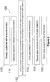
- a preferred processing method is schematically illustrated in a flowchart 100 shown in Figure 4 and will be described in detail below. It has, however, to be understood that this is only an example of a suitable method for forming a device according to the invention and that the sequence of the process steps as described hereinafter is not limiting the invention.
- a substrate 1 is provided.
- said substrate 1 is a semiconductor substrate such as a silicon substrate or a silicon on insulator (SOI) substrate but any other suitable substrate can be used as well such as, for example, glass, ceramics, etc.
- a source contact 2 is created in said substrate 1 or alternatively on top of said substrate.
- the source contact 2 may be made of a conductive material, e.g. said source contact 2, may be a silicide containing structure (NiSi, CoSi 2 , TiSi 2 ...), a germanide containing structure, a metal containing structure, polysilicon or a combination thereof.
- source contacts 2 formed of e.g.
- the source contact 2 is a metal containing structure, all metals which form an ohmic contact with the material of a nanowire, or in other words all metals having a comparable work function with respect to the work function of the material of the nanowire, are preferred metals and may be used according to the invention.
- the source contact 2 is a silicide containing structure.
- the source contact 2 can be the starting point for growing the nanowire and can, at the same time, act as the catalyst for the nanowire growth. However, the latter is not necessarily essential.
- the source contact can not be used as a catalyst for the subsequent nanowire growth
- a catalyst needs to be deposited onto the source contact, step 111.
- the requirement of catalyst particles also depends on the technique used to form the nanowire.
- a nanowire is grown, a preferred method is e.g. by means of a VLS (Vapor-Liquid-Solid) process, but also any other suitable technique known by a person skilled in the art may be used to form the nanowires according to the invention.
- the nanowire may be grown using techniques such as, for example, CVD (Chemical Vapor Deposition), MOCVD (Metal Organic Chemical Vapor Deposition), or PECVD (plasma enhanced chemical vapor deposition) processes.
- CVD Chemical Vapor Deposition
- MOCVD Metal Organic Chemical Vapor Deposition
- PECVD plasma enhanced chemical vapor deposition
- PLD Pulsed Laser Deposition
- ECD Electrochemical Deposition
- e-beam or MBE Molecular Beam Epitaxy
- the source region 3 the channel region 4, the drain region 5 and the heterosection 9 of the nanowire.
- the different regions in the nanowire can be doped during the growth process to obtain a n-type or p-type region.
- the doping of the nanowire may be performed after growth of the nanowire by means of an additional doping step.
- the doping in one specific region, e.g. source region/ drain region is preferably uniform, but may also have a non-uniform doping profile.
- a source region 3 needs to be created.
- Said source region 3 is made of a first semiconductor material which is highly p doped in case of a n-type NW-TFET, or alternatively in case of a p-type NW-TFET said source region is highly n doped. More preferred the doping level of the source region is in the range of 10 18 /cc to 10 21 /cc. Most preferred the doping level of the source region is in the range of 10 19 /cc to 5.10 20 /cc.
- a heterosection 9 is formed onto the source region 3.
- the heterosection 9 is made of a second semiconductor material which is such that it has a different lattice constant compared to the first semiconductor material used to form the source region 3 of the nanowire.
- Said second semiconductor material is highly doped and is selected from at least one of the group IV materials such as Si, Ge, C and binary compounds thereof, or group III/V materials such as In, Ga, As, Sb, Al, P, B, N and binary, tertiary and quaternary compounds thereof or group II/VI materials such as Cd, Zn, S, Se, Te, O and binary, tertiary and quaternary compounds thereof.
- the doping level of the heterosection is preferably in the range of 10 18 /cc to 10 21 /cc, more preferred the doping level of the heterosection is in the range of 10 19 /cc to 5x10 20 /cc.
- said heterosection can be made of metals (Al, W, Ta, Ti, Ru, Pd, Rh, Re, Pt, and alloys thereof), silicides, germanides, metal-nitrides such as TaN and TiN, conductive oxides such as RuO 2 and ReO 2 , silicided metals such as CoSi 2 , NiSi 2 , metal germanides and alloys and mixtures thereof.
- the channel region of the NW-TFET is formed in the nanowire, said channel region is preferably made of the first semiconductor material, although other suitable/compatible materials can be used.
- the doping level of the channel region is in the range of undoped up to 10 16 /cc doping. More preferred the doping level of the channel region is in the range of undoped up to 10 14 /cc doping.
- a drain region 5 needs to be created on top of the channel region.
- Said drain region 5 is made of a first semiconductor material which is highly n doped in case of a n-type NW-TFET (or alternatively in case of a n-type NW-TFET said drain region 5 is highly p doped. More preferred the doping level of the drain region is in the range of 10 18 /cc to 10 21 /cc. Most preferred the doping level of the drain region is in the range of 10 19 /cc to 5.10 20 /cc.
- a gate structure needs to be formed onto the sidewalls of the nanowire, more specifically onto the sidewalls of the channel region of the nanowire.
- Said gate structure comprises a gate oxide 8 (also referred to as gate dielectric) and a gate electrode 7 (also referred to as gate contact).
- the gate oxide 8 is formed and deposited directly onto the channel region 4 of the nanowire 113. Most preferred, said gate oxide 8 completely covers the outer sidewalls of the channel region 4. To obtain a complete coverage of the channel region, a small overlap of the gate oxide with the highly-doped drain and source region is desirable.
- the gate oxide can be restricted to part of the nanowire (i.e.
- a sacrificial layer which is etched away before the oxide deposition (this implies that e.g. other materials are deposited onto the wafer after nanowire growth, such that the nanowire is embedded in other materials. This should be done in such a way that a sacrificial layer lines up with the channel region of the nanowire.
- a dielectric e.g. an oxide, can be deposited onto the nanowire channel region.
- a gate contact (electrode) is deposited, step 114, said gate contact is deposited on top of said gate dielectric, e.g. gate oxide, and is preferably covering the whole gate oxide.
- the gate dielectric is preferably selected from at least one of silicon based oxide (e.g. silicon dioxide, silicon oxy nitride) aluminium oxide, high-k oxides (oxides, nitrided oxides), silicates and nitrided silicates of transition metals such as Hf, Ta, Ti, Nb, V, Y, Zr. Most preferred said gate oxide is a high-k oxide such as hafnium oxide.
- the thickness of the gate oxide is preferably in the range of 0.5 nm to 20 nm.
- the gate contact is preferably made of a conductive material and is preferably selected from at least one of poly silicon, poly germanium, metals such as Al, W, Ta, Ti, Ru, Pd, Rh, Re, Pt, and alloys thereof, metal-nitrides such as TaN and TiN, metal-silicon nitrides such as TaSiN, conductive oxides such as RuO 2 and ReO 3 , fully silicided metals (FUSI) such as CoSi 2 , NiSi and TiSi 2 , fully germanided metals (FUGE), workfunction tunable metals, engineered materials to obtain a particular gate workfunction.
- Most preferred said gate contact is made of a metal of which the workfunction has been engineered specifically for the chosen nanowire material, the gate oxide material and gate oxide thickness.
- Said electrical contact is preferably a conductive material which is selected from at least one of a silicide containing structure (NiSi, CoSi 2 , TiSi 2 ,...), a germanide containing structure, a metal containing structure, poly silicon or a combination thereof. Most preferred said electrical contact is a combination of a metal with a silicide.
- an extra doping step may be advantageous.
- implantation of dopant elements followed by activation of the dopant elements by e.g. annealing can be applied to achieve n-type or p-type region in the nanowire.
- a layer, which is also referred to as dopant layer and which comprises dopant elements can be deposited or a dopant metal can be selectively deposited, e.g. with electrochemical deposition, onto the nanowire regions (not shown).
- An anneal step may then be applied so as to incorporate the dopant into the nanowire region, resulting in an n-type or p-type region.
- the whole processing sequence to obtain a NW-TFET, in the example shown in Figure 2 for a n-type NW-TFET, as described in the previous steps can be repeated to build a second NW-TFET structure on top of the existing NW-TFET structure starting on the drain contact.
- the first NW-TFET structure is a n-type NW-TFET structure
- the second structure may preferably be a p-type NW-TFET structure.
- TFETs typically suffer from low on-currents, a drawback related to the large resistance of the tunnel barrier.
- This simulation illustrated below demonstrates that high on-currents can be achieved for a TFET with a germanium (Ge) tunnel barrier in an otherwise silicon (Si) channel.
- Ge germanium
- Si silicon
- the simulations predict a dynamic power reduction of up to a factor of at least 5, as well as a static power reduction of at least a factor of 2 compared to conventional MOSFET configurations. Multiple layers of logic can therefore be envisioned with these nanowire Si/Ge TFETs resulting in ultra-high on-chip transistor densities.
- the simulations are performed with device simulator "MEDICI" to determine the characteristics of a (silicon) NW-TFET with a highly-doped Ge section at the tunnel barrier.
- the NW-TFET used for the simulation is shown in Figure 6A .
- the NW-TFET structure is 2-dimensional and has a double-gate.
- the height of the central part (between the oxides) is 100 nm, and the height of the hafnium oxide is 4 nm.
- the width of the highly p-doped section is 65 nm
- the heterosection is 3 nm
- the width of the channel region is 100 nm
- the width of the highly n-doped section is 44 nm.
- the 3 nm heterosection is made of either Si, Si 0.5 Ge 0.5 or Ge.
- the NW-TFET structure can be fabricated using the state of the art technology taking into account that nanowires can cope with the lattice mismatch between silicon and germanium.
- the most important dimensions in the NW-TFET structure to be taken into account for the electrical performance are the oxide thickness and the width of the channel region. Further parameters of importance are the doping of the source and drain sections, as well as the material used for the heterosection. The doping of the channel region is not critical, as long as it is lowly doped.
- the doping concentrations and dopant type in the NW-TFET used to perform the simulations are summarized in Table 1. Table 2: Doping concentrations and dopant type in the NW-TFET used to perform the simulations.
- the electrical characteristics of the NW-TFET structure as shown in Figure 6A are presented in Figure 6B .
- the source-drain current is the current underneath one of the double-gates only, to allow a fair comparison with a single-gate MOSFET structure. It can be observed that all devices can be turned off properly (see off-current requirements in Table 2). To achieve an on-current of 0.93 mA/ ⁇ m (target for LOP, which is the most important design strategy, see Table 2) with the all-silicon NW-TFET would require very high gate voltages, as can be observed. However, for the NW-TFET with the Ge-section, such currents can be achieved at very low gate voltages.
- Table 2 International Technology Roadmap for Semiconductors (ITRS) roadmap values for node 14 (year 2020) of the on-current and off-current of a MOSFET for different design approaches.
- Design strategy NMOS drive current source-drain off-current Low operating power (LOP) 0.930 mA/ ⁇ m 20 nA/ ⁇ m Low stand-by power (LSTP) 1.3-1.4 mA/ ⁇ m 100-160 pA/ ⁇ m High performance (HP) 3 mA/ ⁇ m 110 nA/ ⁇ m
- the proposed NW-TFET structure therefore fulfills the ITRS requirements of node 14 (year 2020) which cannot be achieved by a conventional MOSFET.
- tunnel field-effect transistors are regarded as successors of metal-oxide semiconductor field-effect transistors (MOSFETs), but silicon-based TFETs typically suffer from low on-currents, a drawback related to the large resistance of the tunnel barrier.
- MOSFETs metal-oxide semiconductor field-effect transistors
- TFET with a germanium (Ge) tunnel barrier in an otherwise silicon (Si) channel is used.
- Ge germanium
- Si silicon
- a nanowire-based structure with a heterosection (9) is introduced such that the lattice mismatch between silicon and germanium does not result in a highly defective interface.
- a dynamic power reduction as well as a static power reduction can result, compared to conventional MOSFET configurations. Multiple layers of logic can therefore be envisioned with these nanowire Si/Ge TFETs resulting in ultra-high on-chip transistor densities.
Landscapes
- Engineering & Computer Science (AREA)
- Chemical & Material Sciences (AREA)
- Nanotechnology (AREA)
- Physics & Mathematics (AREA)
- Mathematical Physics (AREA)
- Theoretical Computer Science (AREA)
- Crystallography & Structural Chemistry (AREA)
- Thin Film Transistor (AREA)
- Insulated Gate Type Field-Effect Transistor (AREA)
- Metal-Oxide And Bipolar Metal-Oxide Semiconductor Integrated Circuits (AREA)
Claims (26)
- Dispositif semi-conducteur à transistor à effet de champ tunnel (TFET) comprenant au moins un nanofil mis à croître sur un substrat (1) (NW-TFET), ledit nanofil comprenant :- une région de source (2) faite d'un premier matériau semi-conducteur qui est hautement dopé selon un premier type de conductivité,- une région de drain (5) faite d'un premier matériau semi-conducteur qui est hautement dopé selon un second type de conductivité,- une région de canal (4) faite d'un premier matériau semi-conducteur ayant un niveau de dopage dans la plage allant de non dopé jusqu'à 1016/cm3 selon le second type de conductivité et qui est située entre les régions de source et de drain, et- une hétérosection (9) faite d'un matériau ayant une constante de maille cristalline différente du premier matériau semi-conducteur qui est située entre la région de source ou la région de drain et la région de canal,- sur la région de canal du nanofil, une structure de grille, ladite structure de grille comprenant un diélectrique de grille (8) avec au sommet dudit diélectrique de grille, un contact de grille (7),dans lequel le diamètre dudit au moins un nanofil est compris entre 1 et 500 nm.
- Transistor à effet de champ tunnel (NW-TFET) selon la revendication 1, dans lequel la structure de grille couvre complètement la région de canal du nanofil.
- Transistor à effet de champ tunnel (NW-TFET) selon l'une quelconque des revendications précédentes, comprenant un contact électrique (2, 6) sur chacune de la région de source et de la région de drain.
- Transistor à effet de champ tunnel (NW-TFET) selon l'une quelconque des revendications précédentes, dans lequel ledit premier matériau semi-conducteur est choisi parmi au moins l'un des matériaux du groupe IV et de leurs composés binaires, ou des matériaux du groupe III/V et de leurs composés binaires, tertiaires et quaternaires, ou des matériaux du groupe II/VI et de leurs composés binaires, tertiaires et quaternaires.
- Transistor à effet de champ tunnel (NW-TFET) selon l'une quelconque des revendications précédentes, dans lequel ledit premier matériau semi-conducteur comprend du silicium.
- Transistor à effet de champ tunnel (NW-TFET) selon l'une quelconque des revendications précédentes, dans lequel ladite hétérosection est faite d'un second matériau semi-conducteur qui a une constante de maille cristalline différente du premier matériau semi-conducteur du nanofil.
- Transistor à effet de champ tunnel (NW-TFET) selon l'une quelconque des revendications précédentes, dans lequel ledit second matériau semi-conducteur est choisi parmi au moins l'un des matériaux du groupe IV et de leurs composés binaires, ou des matériaux du groupe III/V et de leurs composés binaires, tertiaires, et quaternaires, ou des matériaux du groupe II/VI et de leurs composés binaires, tertiaires, et quaternaires.
- Transistor à effet de champ tunnel (NW-TFET) selon l'une quelconque des revendications précédentes, dans lequel ledit second matériau semi-conducteur comprend du germanium ou Si1-xGex avec x > 0,5.
- Transistor à effet de champ tunnel (NW-TFET) selon les revendications 1 à 5, dans lequel ladite hétérosection est choisie parmi au moins l'un du groupe des métaux (Al, W, Ta, Ti, Ru, Pd, Rh, Re, Pt, et leurs alliages), les siliciures, les germaniures, les nitrures de métal, les oxydes conducteurs, les métaux siliciurés, les germaniures de métal et leurs alliages et mélanges.
- Transistor à effet de champ tunnel (NW-TFET) selon l'une quelconque des revendications précédentes, dans lequel la longueur de l'au moins un nanofil est comprise entre 5 nm et 2 µm, de préférence entre 10 nm et 1 µm.
- Transistor à effet de champ tunnel (NW-TFET) selon l'une quelconque des revendications précédentes, dans lequel ledit diélectrique de grille est choisi parmi au moins l'un d'un oxyde à base de silicium, de l'oxyde d'aluminium, d'oxydes à k élevée, de silicates et de silicates nitrurés de métaux de transition.
- Transistor à effet de champ tunnel (NW-TFET) selon la revendication 11, dans lequel ledit diélectrique de grille est de l'oxyde d'hafnium.
- Transistor à effet de champ tunnel (NW-TFET) selon l'une quelconque des revendications précédentes, dans lequel ledit contact de grille est fait d'un matériau conducteur et est choisi parmi au moins l'un du polysilicium, du polygermanium, d'un métal ou d'un alliage de métal, de nitrures de métaux, de nitrures de métal-silicium, d'oxydes conducteurs, de métaux totalement siliciurés, de métaux totalement germaniurés, de métaux à travail d'extraction ajustable, de matériaux d'ingénierie pour obtenir une fonction d'extraction de grille particulière.
- Transistor à effet de champ tunnel (NW-TFET) selon l'une quelconque des revendications précédentes, dans lequel ledit contact de grille est fait d'un métal dont la fonction d'extraction a été mise au point spécifiquement pour le premier et le second matériau semi-conducteur, le diélectrique de grille et l'épaisseur du diélectrique de grille.
- Transistor à effet de champ tunnel (NW-TFET) selon l'une quelconque des revendications précédentes, dans lequel ledit contact électrique sur chacune de la région de source et de la région de drain est un matériau conducteur qui est choisi parmi au moins l'une parmi une structure contenant du siliciure, une structure contenant du germaniure, une structure contenant du métal, du polysilicium ou l'une de leurs combinaisons.
- Transistor à effet de champ tunnel (NW-TFET) selon l'une quelconque des revendications précédentes, dans lequel ledit contact électrique sur chacune de la région de source et de la région de drain est une combinaison d'un métal avec un siliciure.
- Transistor à effet de champ tunnel (NW-TFET) selon l'une quelconque des revendications précédentes, dans lequel la longueur de ladite hétérosection est dans la plage de 1 nm jusqu'à 50 nm, de préférence dans la plage de 2 nm à 10 nm.
- Transistor à effet de champ tunnel (NW-TFET) selon l'une quelconque des revendications précédentes, dans lequel la longueur de ladite région de canal est dans la plage de 1 nm à 1 000 nm, de préférence dans la plage de 1 nm à 100 nm.
- Transistor à effet de champ tunnel (NW-TFET) selon l'une quelconque des revendications précédentes, dans lequel l'épaisseur du diélectrique de grille est dans la plage de 0,5 nm à 20 nm.
- Transistor à effet de champ tunnel (NW-TFET) selon l'une quelconque des revendications précédentes, dans lequel le niveau de dopage de la région de source et de la région de drain est dans la plage de 1018/cm3 à 1021/cm3, de préférence dans la plage de 1019/cm3 à 5 x 10²⁰/cm3.
- Transistor à effet de champ tunnel (NW-TFET) selon l'une quelconque des revendications précédentes, dans lequel le niveau de dopage de l'hétérosection est dans la plage de 1018/cm3 à 1021/cm3, de préférence dans la plage de 1019/cm3 à 5 x 10²⁰/cm3.
- Transistor à effet de champ tunnel (NW-TFET) selon l'une quelconque des revendications précédentes, dans lequel le niveau de dopage de la région de canal est dans la plage allant de non dopé jusqu'à 1014/cm3 de dopage.
- Procédé de fabrication d'un dispositif semi-conducteur à transistor à effet de champ tunnel à nanofil (NW-TFET) comprenant les étapes de :- fourniture d'un substrat (1) reposant dans un plan,- fourniture d'un contact de source (2) sur ledit substrat (1),- croissance d'une structure de nanofil avec un diamètre de l'au moins un nanofil entre 1 et 500 nm, ledit nanofil ayant une région de source intégrée (3), une région de canal (4) ayant un niveau de dopage dans la plage allant de non dopé jusqu'à 1016/cm3, une hétérosection (9) et une région de drain (5), dans lequel lesdites région de source, région de canal et région de drain sont faites d'un premier matériau semi-conducteur et l'hétérosection est faite d'un second matériau avec une constante de maille cristalline différente du premier matériau semi-conducteur,- dopage sélectif desdites région de source (3), région de canal (4), hétérosection (9) et région de drain (5) à un niveau de dopage et un type de dopant souhaités,- dépôt sur des parois latérales de la structure de nanofil d'un diélectrique de grille (8),- dépôt au sommet du diélectrique de grille d'un contact de grille (7),- formation d'un contact de drain (6) au sommet de la région de drain du nanofil.
- Procédé selon la revendication 23, dans lequel ledit substrat est une tranche de Si.
- Procédé selon l'une quelconque des revendications 23 ou 24, dans lequel après fourniture sur ledit substrat (1) d'un contact de source (2), un catalyseur est déposé.
- Utilisation du procédé de l'une quelconque des revendications 23 à 25, pour former un dispositif semi-conducteur à transistor à effet de champ tunnel à nanofil (NW-TFET) selon l'une quelconque des revendications 1 à 22.
Priority Applications (4)
| Application Number | Priority Date | Filing Date | Title |
|---|---|---|---|
| EP07010947.5A EP1901354B1 (fr) | 2006-09-15 | 2007-06-04 | Transistor à effet de champ de tunnel et barrière de tunnel commandée par la grille. |
| US11/765,945 US7893476B2 (en) | 2006-09-15 | 2007-06-20 | Tunnel effect transistors based on silicon nanowires |
| JP2007218542A JP5171161B2 (ja) | 2006-09-15 | 2007-08-24 | ナノワイヤトンネル電界効果トランジスタ半導体装置およびその製造方法 |
| EP07075809.9A EP1901355B1 (fr) | 2006-09-15 | 2007-09-17 | Transistors à effet tunnel basés sur des nanofils monocristallins ayant une hétérostructure |
Applications Claiming Priority (1)
| Application Number | Priority Date | Filing Date | Title |
|---|---|---|---|
| US84500606P | 2006-09-15 | 2006-09-15 |
Publications (2)
| Publication Number | Publication Date |
|---|---|
| EP1900681A1 EP1900681A1 (fr) | 2008-03-19 |
| EP1900681B1 true EP1900681B1 (fr) | 2017-03-15 |
Family
ID=37944533
Family Applications (1)
| Application Number | Title | Priority Date | Filing Date |
|---|---|---|---|
| EP06024507.3A Not-in-force EP1900681B1 (fr) | 2006-09-15 | 2006-11-27 | Transistors à effet de champ et effet tunnel à base de nanofils de silicium |
Country Status (3)
| Country | Link |
|---|---|
| US (2) | US8072012B2 (fr) |
| EP (1) | EP1900681B1 (fr) |
| JP (2) | JP2008103702A (fr) |
Cited By (1)
| Publication number | Priority date | Publication date | Assignee | Title |
|---|---|---|---|---|
| KR20220045018A (ko) * | 2019-08-15 | 2022-04-12 | 마이크론 테크놀로지, 인크 | 2차원 재료들을 포함하는 집적 조립체들 |
Families Citing this family (59)
| Publication number | Priority date | Publication date | Assignee | Title |
|---|---|---|---|---|
| EP1900681B1 (fr) | 2006-09-15 | 2017-03-15 | Imec | Transistors à effet de champ et effet tunnel à base de nanofils de silicium |
| US7893476B2 (en) * | 2006-09-15 | 2011-02-22 | Imec | Tunnel effect transistors based on silicon nanowires |
| US7812370B2 (en) | 2007-07-25 | 2010-10-12 | Taiwan Semiconductor Manufacturing Company, Ltd. | Tunnel field-effect transistor with narrow band-gap channel and strong gate coupling |
| US7834345B2 (en) * | 2008-09-05 | 2010-11-16 | Taiwan Semiconductor Manufacturing Company, Ltd. | Tunnel field-effect transistors with superlattice channels |
| US8587075B2 (en) * | 2008-11-18 | 2013-11-19 | Taiwan Semiconductor Manufacturing Company, Ltd. | Tunnel field-effect transistor with metal source |
| US8674451B2 (en) * | 2008-12-10 | 2014-03-18 | Taiwan Semiconductor Manufacturing Company, Ltd. | N/P metal crystal orientation for high-K metal gate Vt modulation |
| US8026509B2 (en) * | 2008-12-30 | 2011-09-27 | Intel Corporation | Tunnel field effect transistor and method of manufacturing same |
| WO2011040012A1 (fr) * | 2009-09-30 | 2011-04-07 | 国立大学法人北海道大学 | Transistor à effet de champ et effet tunnel et procédé de fabrication associé |
| EP2309544B1 (fr) * | 2009-10-06 | 2019-06-12 | IMEC vzw | Transistor à effet de champ à effet tunnel doté d'une oscillation infraliminaire améliorée |
| US8143113B2 (en) | 2009-12-04 | 2012-03-27 | International Business Machines Corporation | Omega shaped nanowire tunnel field effect transistors fabrication |
| US8129247B2 (en) * | 2009-12-04 | 2012-03-06 | International Business Machines Corporation | Omega shaped nanowire field effect transistors |
| US8455334B2 (en) | 2009-12-04 | 2013-06-04 | International Business Machines Corporation | Planar and nanowire field effect transistors |
| US8384065B2 (en) * | 2009-12-04 | 2013-02-26 | International Business Machines Corporation | Gate-all-around nanowire field effect transistors |
| US8173993B2 (en) * | 2009-12-04 | 2012-05-08 | International Business Machines Corporation | Gate-all-around nanowire tunnel field effect transistors |
| US8097515B2 (en) * | 2009-12-04 | 2012-01-17 | International Business Machines Corporation | Self-aligned contacts for nanowire field effect transistors |
| US8263477B2 (en) | 2010-01-08 | 2012-09-11 | International Business Machines Corporation | Structure for use in fabrication of PiN heterojunction TFET |
| US8722492B2 (en) | 2010-01-08 | 2014-05-13 | International Business Machines Corporation | Nanowire pin tunnel field effect devices |
| US8324940B2 (en) | 2010-04-13 | 2012-12-04 | International Business Machines Corporation | Nanowire circuits in matched devices |
| EP2378557B1 (fr) | 2010-04-19 | 2015-12-23 | Imec | Procédé de fabrication d'un TFET vertical |
| US8361907B2 (en) | 2010-05-10 | 2013-01-29 | International Business Machines Corporation | Directionally etched nanowire field effect transistors |
| US8324030B2 (en) | 2010-05-12 | 2012-12-04 | International Business Machines Corporation | Nanowire tunnel field effect transistors |
| FR2962850B1 (fr) * | 2010-07-19 | 2012-08-17 | Commissariat Energie Atomique | Dispositif et procede pour former sur un nanofil en semi-conducteur un alliage de ce semi-conducteur avec un metal ou un metalloide. |
| US8835231B2 (en) | 2010-08-16 | 2014-09-16 | International Business Machines Corporation | Methods of forming contacts for nanowire field effect transistors |
| US8536563B2 (en) | 2010-09-17 | 2013-09-17 | International Business Machines Corporation | Nanowire field effect transistors |
| US8890118B2 (en) | 2010-12-17 | 2014-11-18 | Intel Corporation | Tunnel field effect transistor |
| WO2012152762A1 (fr) | 2011-05-06 | 2012-11-15 | Imec | Dispositif à transistor à effet de champ et à effet tunnel |
| EP2528099B1 (fr) * | 2011-05-23 | 2015-03-04 | Imec | Transistor tunnel à effet de champ (TFET) à effet tunnel en ligne et procédé de fabrication |
| US8872230B2 (en) * | 2011-12-21 | 2014-10-28 | Imec | Tunnel field-effect transistor and methods for manufacturing thereof |
| US9142400B1 (en) | 2012-07-17 | 2015-09-22 | Stc.Unm | Method of making a heteroepitaxial layer on a seed area |
| US8890120B2 (en) | 2012-11-16 | 2014-11-18 | Intel Corporation | Tunneling field effect transistors (TFETs) for CMOS approaches to fabricating N-type and P-type TFETs |
| US8890119B2 (en) | 2012-12-18 | 2014-11-18 | Intel Corporation | Vertical nanowire transistor with axially engineered semiconductor and gate metallization |
| US8896101B2 (en) | 2012-12-21 | 2014-11-25 | Intel Corporation | Nonplanar III-N transistors with compositionally graded semiconductor channels |
| JP6083704B2 (ja) * | 2013-03-25 | 2017-02-22 | 国立研究開発法人産業技術総合研究所 | トンネルfetのデバイスシミュレーション方法及びシステム並びにトンネルfetのコンパクトモデル設計方法及びコンパクトモデル |
| WO2014209332A1 (fr) * | 2013-06-27 | 2014-12-31 | Intel Corporation | Transistors à effet tunnel de champ (tfets) comportant des régions enroulées à recouvrement négatif de purge non dopées |
| US8975123B2 (en) | 2013-07-09 | 2015-03-10 | International Business Machines Corporation | Tunnel field-effect transistors with a gate-swing broken-gap heterostructure |
| EP2858117A1 (fr) * | 2013-10-02 | 2015-04-08 | Nxp B.V. | Dispositif semi-conducteur et procédé de fabrication |
| WO2015099744A1 (fr) * | 2013-12-26 | 2015-07-02 | Intel Corporation | Dispositifs fet à effet tunnel complémentaires et leur procédé de formation |
| CN104752501B (zh) * | 2013-12-27 | 2018-05-04 | 中芯国际集成电路制造(上海)有限公司 | 一种半导体器件及其制造方法 |
| CN106030817B (zh) * | 2014-03-28 | 2019-11-22 | 英特尔公司 | 具有可变带隙沟道的隧穿场效应晶体管 |
| WO2015147865A1 (fr) * | 2014-03-28 | 2015-10-01 | Intel Corporation | Piégeage selon le rapport de forme (art) pour fabriquer des dispositifs à semi-conducteur verticaux |
| JP5989238B2 (ja) * | 2014-08-28 | 2016-09-07 | ユニサンティス エレクトロニクス シンガポール プライベート リミテッドUnisantis Electronics Singapore Pte Ltd. | 半導体装置、及び、半導体装置の製造方法 |
| EP2993696B1 (fr) | 2014-09-02 | 2020-08-05 | IMEC vzw | Transistor TFET (Heterosection Tunnel Field-Effect) |
| US9871111B2 (en) * | 2014-09-18 | 2018-01-16 | Taiwan Semiconductor Manufacturing Company, Ltd. | Semiconductor device and method |
| EP3010044B1 (fr) * | 2014-10-13 | 2019-02-13 | IMEC vzw | Structure en couches de p-TFET |
| CN105633147A (zh) * | 2014-10-27 | 2016-06-01 | 中国科学院微电子研究所 | 隧穿场效应晶体管及其制造方法 |
| CN104465737B (zh) * | 2014-12-08 | 2017-07-21 | 沈阳工业大学 | 体硅双栅绝缘隧穿基极双极晶体管及其制造方法 |
| CN104576723B (zh) * | 2015-01-22 | 2017-09-12 | 湘潭大学 | 一种具有高开态电流的n型隧穿场效应晶体管 |
| US9614042B2 (en) | 2015-03-06 | 2017-04-04 | International Business Machines Corporation | Heterojunction tunnel field effect transistor fabrication using limited lithography steps |
| US10504721B2 (en) | 2015-04-30 | 2019-12-10 | Taiwan Semiconductor Manufacturing Company, Ltd. | Staggered-type tunneling field effect transistor |
| CN106601738B (zh) * | 2015-10-15 | 2018-08-24 | 上海新昇半导体科技有限公司 | 互补场效应晶体管及其制备方法 |
| CN105390531B (zh) * | 2015-10-27 | 2018-02-13 | 北京大学 | 一种隧穿场效应晶体管的制备方法 |
| WO2017086921A1 (fr) * | 2015-11-16 | 2017-05-26 | Intel Corporation | Transistors à effet de champ tunnel à hétérojonction employant un oxyde semi-conducteur |
| US9735267B1 (en) | 2016-01-28 | 2017-08-15 | Taiwan Semiconductor Manufacturing Co., Ltd. | Structure and formation method of semiconductor device structure |
| US10833193B2 (en) | 2016-09-30 | 2020-11-10 | Institute of Microelectronics, Chinese Academy of Sciences | Semiconductor device, method of manufacturing the same and electronic device including the device |
| CN106298778A (zh) | 2016-09-30 | 2017-01-04 | 中国科学院微电子研究所 | 半导体器件及其制造方法及包括该器件的电子设备 |
| WO2020076759A1 (fr) | 2018-10-09 | 2020-04-16 | Micron Technology, Inc. | Transistors comprenant des canaux hétérogènes, et dispositifs, systèmes électroniques et procédés associés |
| US11133226B2 (en) * | 2018-10-22 | 2021-09-28 | Taiwan Semiconductor Manufacturing Company, Ltd. | FUSI gated device formation |
| US11107817B2 (en) * | 2019-03-11 | 2021-08-31 | Micron Technology, Inc. | Integrated assemblies comprising hydrogen diffused within two or more different semiconductor materials, and methods of forming integrated assemblies |
| TWI854564B (zh) * | 2023-03-30 | 2024-09-01 | 華邦電子股份有限公司 | 半導體裝置及其形成方法 |
Family Cites Families (36)
| Publication number | Priority date | Publication date | Assignee | Title |
|---|---|---|---|---|
| JP3149030B2 (ja) * | 1991-06-13 | 2001-03-26 | 富士通株式会社 | 半導体量子箱装置及びその製造方法 |
| US5471075A (en) | 1994-05-26 | 1995-11-28 | North Carolina State University | Dual-channel emitter switched thyristor with trench gate |
| JP2643890B2 (ja) * | 1994-12-29 | 1997-08-20 | 日本電気株式会社 | トンネルトランジスタ |
| JP4003981B2 (ja) * | 1996-03-25 | 2007-11-07 | 株式会社東芝 | 半導体装置 |
| JP4208281B2 (ja) * | 1998-02-26 | 2009-01-14 | キヤノン株式会社 | 積層型光起電力素子 |
| JP3420972B2 (ja) * | 1999-06-29 | 2003-06-30 | 株式会社東芝 | 半導体装置 |
| JP2001284598A (ja) * | 2000-03-31 | 2001-10-12 | Fujitsu Ltd | 半導体装置及びその製造方法 |
| JP2002110989A (ja) * | 2000-09-27 | 2002-04-12 | Japan Science & Technology Corp | 半導体集積回路装置およびその製造方法 |
| US6996147B2 (en) * | 2001-03-30 | 2006-02-07 | The Regents Of The University Of California | Methods of fabricating nanostructures and nanowires and devices fabricated therefrom |
| DE10118405A1 (de) * | 2001-04-12 | 2002-10-24 | Infineon Technologies Ag | Heterostruktur-Bauelement |
| US7084507B2 (en) * | 2001-05-02 | 2006-08-01 | Fujitsu Limited | Integrated circuit device and method of producing the same |
| US7385262B2 (en) * | 2001-11-27 | 2008-06-10 | The Board Of Trustees Of The Leland Stanford Junior University | Band-structure modulation of nano-structures in an electric field |
| EP1341184B1 (fr) * | 2002-02-09 | 2005-09-14 | Samsung Electronics Co., Ltd. | Dispositif memoire utilisant des nanotubes de carbon et procédé pour son fabrication |
| US7335908B2 (en) * | 2002-07-08 | 2008-02-26 | Qunano Ab | Nanostructures and methods for manufacturing the same |
| US7355216B2 (en) | 2002-12-09 | 2008-04-08 | The Regents Of The University Of California | Fluidic nanotubes and devices |
| JP2004193203A (ja) * | 2002-12-09 | 2004-07-08 | Matsushita Electric Ind Co Ltd | 電界効果トランジスタおよびその製造方法 |
| JP4108537B2 (ja) * | 2003-05-28 | 2008-06-25 | 富士雄 舛岡 | 半導体装置 |
| US7473967B2 (en) * | 2003-05-30 | 2009-01-06 | Panasonic Corporation | Strained channel finFET device |
| JP2005310921A (ja) * | 2004-04-19 | 2005-11-04 | Okayama Prefecture | Mos型半導体装置及びその製造方法 |
| US7180107B2 (en) * | 2004-05-25 | 2007-02-20 | International Business Machines Corporation | Method of fabricating a tunneling nanotube field effect transistor |
| KR100615233B1 (ko) * | 2004-07-21 | 2006-08-25 | 삼성에스디아이 주식회사 | 박막 트랜지스터, 및 이를 구비한 평판 표시장치 |
| JP4488870B2 (ja) * | 2004-11-19 | 2010-06-23 | 株式会社東芝 | 半導体素子と半導体装置 |
| US7629629B2 (en) * | 2004-12-28 | 2009-12-08 | Panasonic Corporation | Semiconductor nanowire and semiconductor device including the nanowire |
| KR100696766B1 (ko) * | 2004-12-29 | 2007-03-19 | 주식회사 하이닉스반도체 | 차지 트랩 인슐레이터 메모리 장치 |
| JP4488947B2 (ja) * | 2005-04-08 | 2010-06-23 | 株式会社東芝 | 不揮発性半導体記憶装置の製造方法 |
| US7465976B2 (en) | 2005-05-13 | 2008-12-16 | Intel Corporation | Tunneling field effect transistor using angled implants for forming asymmetric source/drain regions |
| US7190050B2 (en) * | 2005-07-01 | 2007-03-13 | Synopsys, Inc. | Integrated circuit on corrugated substrate |
| US7446372B2 (en) | 2005-09-01 | 2008-11-04 | Micron Technology, Inc. | DRAM tunneling access transistor |
| US8441000B2 (en) * | 2006-02-01 | 2013-05-14 | International Business Machines Corporation | Heterojunction tunneling field effect transistors, and methods for fabricating the same |
| US7692973B2 (en) * | 2006-03-31 | 2010-04-06 | Semiconductor Energy Laboratory Co., Ltd | Semiconductor device |
| US7425491B2 (en) * | 2006-04-04 | 2008-09-16 | Micron Technology, Inc. | Nanowire transistor with surrounding gate |
| US7491995B2 (en) | 2006-04-04 | 2009-02-17 | Micron Technology, Inc. | DRAM with nanofin transistors |
| US7714386B2 (en) * | 2006-06-09 | 2010-05-11 | Northrop Grumman Systems Corporation | Carbon nanotube field effect transistor |
| US7893476B2 (en) * | 2006-09-15 | 2011-02-22 | Imec | Tunnel effect transistors based on silicon nanowires |
| EP1900681B1 (fr) | 2006-09-15 | 2017-03-15 | Imec | Transistors à effet de champ et effet tunnel à base de nanofils de silicium |
| JP5400280B2 (ja) * | 2007-06-07 | 2014-01-29 | パナソニック株式会社 | 固体撮像装置 |
-
2006
- 2006-11-27 EP EP06024507.3A patent/EP1900681B1/fr not_active Not-in-force
-
2007
- 2007-09-14 US US11/855,930 patent/US8072012B2/en not_active Expired - Fee Related
- 2007-09-18 JP JP2007241505A patent/JP2008103702A/ja active Pending
-
2011
- 2011-11-01 US US13/286,936 patent/US8148220B2/en not_active Expired - Fee Related
-
2014
- 2014-07-10 JP JP2014142336A patent/JP5695255B2/ja not_active Expired - Fee Related
Non-Patent Citations (2)
| Title |
|---|
| BHUWALKA K K ET AL: "A Simulation Approach to Optimize the Electrical Parameters of a Vertical Tunnel FET", IEEE TRANSACTIONS ON ELECTRON DEVICES, IEEE SERVICE CENTER, PISACATAWAY, NJ, US, vol. 52, no. 7, 1 July 2005 (2005-07-01), pages 1541 - 1547, XP011135503, ISSN: 0018-9383, DOI: 10.1109/TED.2005.850618 * |
| KRISHNA KUMAR BHUWALKA ET AL: "VERTICAL TUNNEL FIELD-EFFECT TRANSISTOR", IEEE TRANSACTIONS ON ELECTRON DEVICES, IEEE SERVICE CENTER, PISACATAWAY, NJ, US, vol. 51, no. 2, 1 February 2004 (2004-02-01), pages 279 - 282, XP001186093, ISSN: 0018-9383, DOI: 10.1109/TED.2003.821575 * |
Cited By (1)
| Publication number | Priority date | Publication date | Assignee | Title |
|---|---|---|---|---|
| KR20220045018A (ko) * | 2019-08-15 | 2022-04-12 | 마이크론 테크놀로지, 인크 | 2차원 재료들을 포함하는 집적 조립체들 |
Also Published As
| Publication number | Publication date |
|---|---|
| US20120045879A1 (en) | 2012-02-23 |
| JP2015019072A (ja) | 2015-01-29 |
| JP2008103702A (ja) | 2008-05-01 |
| US8148220B2 (en) | 2012-04-03 |
| US8072012B2 (en) | 2011-12-06 |
| US20080067607A1 (en) | 2008-03-20 |
| EP1900681A1 (fr) | 2008-03-19 |
| JP5695255B2 (ja) | 2015-04-01 |
Similar Documents
| Publication | Publication Date | Title |
|---|---|---|
| US7893476B2 (en) | Tunnel effect transistors based on silicon nanowires | |
| US8148220B2 (en) | Tunnel effect transistors based on elongate monocrystalline nanostructures having a heterostructure | |
| US8120115B2 (en) | Tunnel field-effect transistor with gated tunnel barrier | |
| EP1901354B1 (fr) | Transistor à effet de champ de tunnel et barrière de tunnel commandée par la grille. | |
| EP2309544B1 (fr) | Transistor à effet de champ à effet tunnel doté d'une oscillation infraliminaire améliorée | |
| US9318583B2 (en) | Tunnel field effect transistor and method for making thereof | |
| US8629428B2 (en) | Line-tunneling tunnel field-effect transistor (TFET) and manufacturing method | |
| JP5171161B2 (ja) | ナノワイヤトンネル電界効果トランジスタ半導体装置およびその製造方法 | |
| US8431924B2 (en) | Control of tunneling junction in a hetero tunnel field effect transistor | |
| US8119488B2 (en) | Scalable quantum well device and method for manufacturing the same | |
| CN101065811B (zh) | 制造隧穿纳米管场效应晶体管的方法 | |
| US8288803B2 (en) | Tunnel field effect devices | |
| EP1901355B1 (fr) | Transistors à effet tunnel basés sur des nanofils monocristallins ayant une hétérostructure | |
| Liu et al. | Vertical heterojunction Ge0. 92Sn0. 08/Ge gate-all-around nanowire pMOSFETs with NiGeSn contact | |
| CN223080386U (zh) | 鳍式场效晶体管装置 | |
| Knoch et al. | Semiconductor nanostructures and devices | |
| Knoll et al. | Unipolar gate-all-around nanowire array p-type tunnelling FETs with 75mV/dec@ VDD= 1.1 V |
Legal Events
| Date | Code | Title | Description |
|---|---|---|---|
| PUAI | Public reference made under article 153(3) epc to a published international application that has entered the european phase |
Free format text: ORIGINAL CODE: 0009012 |
|
| 17P | Request for examination filed |
Effective date: 20070622 |
|
| AK | Designated contracting states |
Kind code of ref document: A1 Designated state(s): AT BE BG CH CY CZ DE DK EE ES FI FR GB GR HU IE IS IT LI LT LU LV MC NL PL PT RO SE SI SK TR |
|
| AX | Request for extension of the european patent |
Extension state: AL BA HR MK YU |
|
| AKX | Designation fees paid |
Designated state(s): AT BE BG CH CY CZ DE DK EE ES FI FR GB GR HU IE IS IT LI LT LU LV MC NL PL PT RO SE SI SK TR |
|
| RAP1 | Party data changed (applicant data changed or rights of an application transferred) |
Owner name: IMEC |
|
| 17Q | First examination report despatched |
Effective date: 20110921 |
|
| RAP1 | Party data changed (applicant data changed or rights of an application transferred) |
Owner name: IMEC Owner name: KATHOLIEKE UNIVERSITEIT LEUVEN |
|
| REG | Reference to a national code |
Ref country code: DE Ref legal event code: R079 Ref document number: 602006051954 Country of ref document: DE Free format text: PREVIOUS MAIN CLASS: B82B0001000000 Ipc: H01L0029739000 |
|
| GRAP | Despatch of communication of intention to grant a patent |
Free format text: ORIGINAL CODE: EPIDOSNIGR1 |
|
| RIC1 | Information provided on ipc code assigned before grant |
Ipc: H01L 29/10 20060101ALI20160919BHEP Ipc: H01L 29/808 20060101ALI20160919BHEP Ipc: H01L 29/06 20060101ALI20160919BHEP Ipc: B82Y 10/00 20110101ALI20160919BHEP Ipc: B82B 1/00 20060101ALI20160919BHEP Ipc: H01L 29/739 20060101AFI20160919BHEP |
|
| RIC1 | Information provided on ipc code assigned before grant |
Ipc: H01L 29/739 20060101AFI20160923BHEP Ipc: B82B 1/00 20060101ALI20160923BHEP Ipc: H01L 29/06 20060101ALI20160923BHEP Ipc: B82Y 10/00 20110101ALI20160923BHEP Ipc: H01L 29/10 20060101ALI20160923BHEP |
|
| INTG | Intention to grant announced |
Effective date: 20161014 |
|
| STAA | Information on the status of an ep patent application or granted ep patent |
Free format text: STATUS: GRANT OF PATENT IS INTENDED |
|
| GRAS | Grant fee paid |
Free format text: ORIGINAL CODE: EPIDOSNIGR3 |
|
| GRAA | (expected) grant |
Free format text: ORIGINAL CODE: 0009210 |
|
| STAA | Information on the status of an ep patent application or granted ep patent |
Free format text: STATUS: THE PATENT HAS BEEN GRANTED |
|
| AK | Designated contracting states |
Kind code of ref document: B1 Designated state(s): AT BE BG CH CY CZ DE DK EE ES FI FR GB GR HU IE IS IT LI LT LU LV MC NL PL PT RO SE SI SK TR |
|
| REG | Reference to a national code |
Ref country code: CH Ref legal event code: EP Ref country code: GB Ref legal event code: FG4D |
|
| REG | Reference to a national code |
Ref country code: IE Ref legal event code: FG4D |
|
| REG | Reference to a national code |
Ref country code: AT Ref legal event code: REF Ref document number: 876365 Country of ref document: AT Kind code of ref document: T Effective date: 20170415 |
|
| REG | Reference to a national code |
Ref country code: DE Ref legal event code: R096 Ref document number: 602006051954 Country of ref document: DE |
|
| REG | Reference to a national code |
Ref country code: NL Ref legal event code: MP Effective date: 20170315 |
|
| REG | Reference to a national code |
Ref country code: LT Ref legal event code: MG4D |
|
| PG25 | Lapsed in a contracting state [announced via postgrant information from national office to epo] |
Ref country code: LT Free format text: LAPSE BECAUSE OF FAILURE TO SUBMIT A TRANSLATION OF THE DESCRIPTION OR TO PAY THE FEE WITHIN THE PRESCRIBED TIME-LIMIT Effective date: 20170315 Ref country code: FI Free format text: LAPSE BECAUSE OF FAILURE TO SUBMIT A TRANSLATION OF THE DESCRIPTION OR TO PAY THE FEE WITHIN THE PRESCRIBED TIME-LIMIT Effective date: 20170315 Ref country code: GR Free format text: LAPSE BECAUSE OF FAILURE TO SUBMIT A TRANSLATION OF THE DESCRIPTION OR TO PAY THE FEE WITHIN THE PRESCRIBED TIME-LIMIT Effective date: 20170616 |
|
| REG | Reference to a national code |
Ref country code: AT Ref legal event code: MK05 Ref document number: 876365 Country of ref document: AT Kind code of ref document: T Effective date: 20170315 |
|
| PG25 | Lapsed in a contracting state [announced via postgrant information from national office to epo] |
Ref country code: SE Free format text: LAPSE BECAUSE OF FAILURE TO SUBMIT A TRANSLATION OF THE DESCRIPTION OR TO PAY THE FEE WITHIN THE PRESCRIBED TIME-LIMIT Effective date: 20170315 Ref country code: LV Free format text: LAPSE BECAUSE OF FAILURE TO SUBMIT A TRANSLATION OF THE DESCRIPTION OR TO PAY THE FEE WITHIN THE PRESCRIBED TIME-LIMIT Effective date: 20170315 Ref country code: BG Free format text: LAPSE BECAUSE OF FAILURE TO SUBMIT A TRANSLATION OF THE DESCRIPTION OR TO PAY THE FEE WITHIN THE PRESCRIBED TIME-LIMIT Effective date: 20170615 |
|
| PG25 | Lapsed in a contracting state [announced via postgrant information from national office to epo] |
Ref country code: NL Free format text: LAPSE BECAUSE OF FAILURE TO SUBMIT A TRANSLATION OF THE DESCRIPTION OR TO PAY THE FEE WITHIN THE PRESCRIBED TIME-LIMIT Effective date: 20170315 |
|
| REG | Reference to a national code |
Ref country code: FR Ref legal event code: PLFP Year of fee payment: 12 |
|
| PG25 | Lapsed in a contracting state [announced via postgrant information from national office to epo] |
Ref country code: RO Free format text: LAPSE BECAUSE OF FAILURE TO SUBMIT A TRANSLATION OF THE DESCRIPTION OR TO PAY THE FEE WITHIN THE PRESCRIBED TIME-LIMIT Effective date: 20170315 Ref country code: ES Free format text: LAPSE BECAUSE OF FAILURE TO SUBMIT A TRANSLATION OF THE DESCRIPTION OR TO PAY THE FEE WITHIN THE PRESCRIBED TIME-LIMIT Effective date: 20170315 Ref country code: IT Free format text: LAPSE BECAUSE OF FAILURE TO SUBMIT A TRANSLATION OF THE DESCRIPTION OR TO PAY THE FEE WITHIN THE PRESCRIBED TIME-LIMIT Effective date: 20170315 Ref country code: SK Free format text: LAPSE BECAUSE OF FAILURE TO SUBMIT A TRANSLATION OF THE DESCRIPTION OR TO PAY THE FEE WITHIN THE PRESCRIBED TIME-LIMIT Effective date: 20170315 Ref country code: AT Free format text: LAPSE BECAUSE OF FAILURE TO SUBMIT A TRANSLATION OF THE DESCRIPTION OR TO PAY THE FEE WITHIN THE PRESCRIBED TIME-LIMIT Effective date: 20170315 Ref country code: CZ Free format text: LAPSE BECAUSE OF FAILURE TO SUBMIT A TRANSLATION OF THE DESCRIPTION OR TO PAY THE FEE WITHIN THE PRESCRIBED TIME-LIMIT Effective date: 20170315 Ref country code: EE Free format text: LAPSE BECAUSE OF FAILURE TO SUBMIT A TRANSLATION OF THE DESCRIPTION OR TO PAY THE FEE WITHIN THE PRESCRIBED TIME-LIMIT Effective date: 20170315 |
|
| PG25 | Lapsed in a contracting state [announced via postgrant information from national office to epo] |
Ref country code: PT Free format text: LAPSE BECAUSE OF FAILURE TO SUBMIT A TRANSLATION OF THE DESCRIPTION OR TO PAY THE FEE WITHIN THE PRESCRIBED TIME-LIMIT Effective date: 20170717 Ref country code: PL Free format text: LAPSE BECAUSE OF FAILURE TO SUBMIT A TRANSLATION OF THE DESCRIPTION OR TO PAY THE FEE WITHIN THE PRESCRIBED TIME-LIMIT Effective date: 20170315 Ref country code: IS Free format text: LAPSE BECAUSE OF FAILURE TO SUBMIT A TRANSLATION OF THE DESCRIPTION OR TO PAY THE FEE WITHIN THE PRESCRIBED TIME-LIMIT Effective date: 20170715 |
|
| REG | Reference to a national code |
Ref country code: DE Ref legal event code: R097 Ref document number: 602006051954 Country of ref document: DE |
|
| RAP2 | Party data changed (patent owner data changed or rights of a patent transferred) |
Owner name: IMEC VZW Owner name: KATHOLIEKE UNIVERSITEIT LEUVEN |
|
| PLBE | No opposition filed within time limit |
Free format text: ORIGINAL CODE: 0009261 |
|
| STAA | Information on the status of an ep patent application or granted ep patent |
Free format text: STATUS: NO OPPOSITION FILED WITHIN TIME LIMIT |
|
| PG25 | Lapsed in a contracting state [announced via postgrant information from national office to epo] |
Ref country code: DK Free format text: LAPSE BECAUSE OF FAILURE TO SUBMIT A TRANSLATION OF THE DESCRIPTION OR TO PAY THE FEE WITHIN THE PRESCRIBED TIME-LIMIT Effective date: 20170315 |
|
| 26N | No opposition filed |
Effective date: 20171218 |
|
| PG25 | Lapsed in a contracting state [announced via postgrant information from national office to epo] |
Ref country code: SI Free format text: LAPSE BECAUSE OF FAILURE TO SUBMIT A TRANSLATION OF THE DESCRIPTION OR TO PAY THE FEE WITHIN THE PRESCRIBED TIME-LIMIT Effective date: 20170315 |
|
| PG25 | Lapsed in a contracting state [announced via postgrant information from national office to epo] |
Ref country code: MC Free format text: LAPSE BECAUSE OF FAILURE TO SUBMIT A TRANSLATION OF THE DESCRIPTION OR TO PAY THE FEE WITHIN THE PRESCRIBED TIME-LIMIT Effective date: 20170315 |
|
| GBPC | Gb: european patent ceased through non-payment of renewal fee |
Effective date: 20171127 |
|
| PG25 | Lapsed in a contracting state [announced via postgrant information from national office to epo] |
Ref country code: CH Free format text: LAPSE BECAUSE OF NON-PAYMENT OF DUE FEES Effective date: 20171130 Ref country code: LI Free format text: LAPSE BECAUSE OF NON-PAYMENT OF DUE FEES Effective date: 20171130 |
|
| PG25 | Lapsed in a contracting state [announced via postgrant information from national office to epo] |
Ref country code: LU Free format text: LAPSE BECAUSE OF NON-PAYMENT OF DUE FEES Effective date: 20171127 |
|
| REG | Reference to a national code |
Ref country code: BE Ref legal event code: MM Effective date: 20171130 |
|
| REG | Reference to a national code |
Ref country code: IE Ref legal event code: MM4A |
|
| REG | Reference to a national code |
Ref country code: FR Ref legal event code: PLFP Year of fee payment: 13 |
|
| PG25 | Lapsed in a contracting state [announced via postgrant information from national office to epo] |
Ref country code: IE Free format text: LAPSE BECAUSE OF NON-PAYMENT OF DUE FEES Effective date: 20171127 |
|
| PG25 | Lapsed in a contracting state [announced via postgrant information from national office to epo] |
Ref country code: GB Free format text: LAPSE BECAUSE OF NON-PAYMENT OF DUE FEES Effective date: 20171127 Ref country code: BE Free format text: LAPSE BECAUSE OF NON-PAYMENT OF DUE FEES Effective date: 20171130 |
|
| PG25 | Lapsed in a contracting state [announced via postgrant information from national office to epo] |
Ref country code: HU Free format text: LAPSE BECAUSE OF FAILURE TO SUBMIT A TRANSLATION OF THE DESCRIPTION OR TO PAY THE FEE WITHIN THE PRESCRIBED TIME-LIMIT; INVALID AB INITIO Effective date: 20061127 |
|
| PG25 | Lapsed in a contracting state [announced via postgrant information from national office to epo] |
Ref country code: CY Free format text: LAPSE BECAUSE OF NON-PAYMENT OF DUE FEES Effective date: 20170315 |
|
| PG25 | Lapsed in a contracting state [announced via postgrant information from national office to epo] |
Ref country code: TR Free format text: LAPSE BECAUSE OF FAILURE TO SUBMIT A TRANSLATION OF THE DESCRIPTION OR TO PAY THE FEE WITHIN THE PRESCRIBED TIME-LIMIT Effective date: 20170315 |
|
| PGFP | Annual fee paid to national office [announced via postgrant information from national office to epo] |
Ref country code: FR Payment date: 20201021 Year of fee payment: 15 Ref country code: DE Payment date: 20201020 Year of fee payment: 15 |
|
| REG | Reference to a national code |
Ref country code: DE Ref legal event code: R119 Ref document number: 602006051954 Country of ref document: DE |
|
| PG25 | Lapsed in a contracting state [announced via postgrant information from national office to epo] |
Ref country code: DE Free format text: LAPSE BECAUSE OF NON-PAYMENT OF DUE FEES Effective date: 20220601 |
|
| PG25 | Lapsed in a contracting state [announced via postgrant information from national office to epo] |
Ref country code: FR Free format text: LAPSE BECAUSE OF NON-PAYMENT OF DUE FEES Effective date: 20211130 |