EP1900859A1 - Composite comprenant un ensemble de cristal aciculaire, son procédé de production, élément de conversion photoélectrique, élément luminescent, et condensateur - Google Patents
Composite comprenant un ensemble de cristal aciculaire, son procédé de production, élément de conversion photoélectrique, élément luminescent, et condensateur Download PDFInfo
- Publication number
- EP1900859A1 EP1900859A1 EP06756852A EP06756852A EP1900859A1 EP 1900859 A1 EP1900859 A1 EP 1900859A1 EP 06756852 A EP06756852 A EP 06756852A EP 06756852 A EP06756852 A EP 06756852A EP 1900859 A1 EP1900859 A1 EP 1900859A1
- Authority
- EP
- European Patent Office
- Prior art keywords
- needle
- crystals
- base
- array
- coating film
- Prior art date
- Legal status (The legal status is an assumption and is not a legal conclusion. Google has not performed a legal analysis and makes no representation as to the accuracy of the status listed.)
- Granted
Links
Images




Classifications
-
- H—ELECTRICITY
- H01—ELECTRIC ELEMENTS
- H01G—CAPACITORS; CAPACITORS, RECTIFIERS, DETECTORS, SWITCHING DEVICES, LIGHT-SENSITIVE OR TEMPERATURE-SENSITIVE DEVICES OF THE ELECTROLYTIC TYPE
- H01G9/00—Electrolytic capacitors, rectifiers, detectors, switching devices, light-sensitive or temperature-sensitive devices; Processes of their manufacture
- H01G9/20—Light-sensitive devices
- H01G9/2027—Light-sensitive devices comprising an oxide semiconductor electrode
- H01G9/2036—Light-sensitive devices comprising an oxide semiconductor electrode comprising mixed oxides, e.g. ZnO covered TiO2 particles
-
- C—CHEMISTRY; METALLURGY
- C25—ELECTROLYTIC OR ELECTROPHORETIC PROCESSES; APPARATUS THEREFOR
- C25B—ELECTROLYTIC OR ELECTROPHORETIC PROCESSES FOR THE PRODUCTION OF COMPOUNDS OR NON-METALS; APPARATUS THEREFOR
- C25B1/00—Electrolytic production of inorganic compounds or non-metals
- C25B1/50—Processes
- C25B1/55—Photoelectrolysis
-
- H—ELECTRICITY
- H01—ELECTRIC ELEMENTS
- H01G—CAPACITORS; CAPACITORS, RECTIFIERS, DETECTORS, SWITCHING DEVICES, LIGHT-SENSITIVE OR TEMPERATURE-SENSITIVE DEVICES OF THE ELECTROLYTIC TYPE
- H01G9/00—Electrolytic capacitors, rectifiers, detectors, switching devices, light-sensitive or temperature-sensitive devices; Processes of their manufacture
- H01G9/20—Light-sensitive devices
- H01G9/2059—Light-sensitive devices comprising an organic dye as the active light absorbing material, e.g. adsorbed on an electrode or dissolved in solution
-
- H—ELECTRICITY
- H10—SEMICONDUCTOR DEVICES; ELECTRIC SOLID-STATE DEVICES NOT OTHERWISE PROVIDED FOR
- H10K—ORGANIC ELECTRIC SOLID-STATE DEVICES
- H10K85/00—Organic materials used in the body or electrodes of devices covered by this subclass
- H10K85/30—Coordination compounds
- H10K85/341—Transition metal complexes, e.g. Ru(II)polypyridine complexes
- H10K85/344—Transition metal complexes, e.g. Ru(II)polypyridine complexes comprising ruthenium
-
- Y—GENERAL TAGGING OF NEW TECHNOLOGICAL DEVELOPMENTS; GENERAL TAGGING OF CROSS-SECTIONAL TECHNOLOGIES SPANNING OVER SEVERAL SECTIONS OF THE IPC; TECHNICAL SUBJECTS COVERED BY FORMER USPC CROSS-REFERENCE ART COLLECTIONS [XRACs] AND DIGESTS
- Y02—TECHNOLOGIES OR APPLICATIONS FOR MITIGATION OR ADAPTATION AGAINST CLIMATE CHANGE
- Y02E—REDUCTION OF GREENHOUSE GAS [GHG] EMISSIONS, RELATED TO ENERGY GENERATION, TRANSMISSION OR DISTRIBUTION
- Y02E10/00—Energy generation through renewable energy sources
- Y02E10/50—Photovoltaic [PV] energy
- Y02E10/542—Dye sensitized solar cells
-
- Y—GENERAL TAGGING OF NEW TECHNOLOGICAL DEVELOPMENTS; GENERAL TAGGING OF CROSS-SECTIONAL TECHNOLOGIES SPANNING OVER SEVERAL SECTIONS OF THE IPC; TECHNICAL SUBJECTS COVERED BY FORMER USPC CROSS-REFERENCE ART COLLECTIONS [XRACs] AND DIGESTS
- Y02—TECHNOLOGIES OR APPLICATIONS FOR MITIGATION OR ADAPTATION AGAINST CLIMATE CHANGE
- Y02P—CLIMATE CHANGE MITIGATION TECHNOLOGIES IN THE PRODUCTION OR PROCESSING OF GOODS
- Y02P70/00—Climate change mitigation technologies in the production process for final industrial or consumer products
- Y02P70/50—Manufacturing or production processes characterised by the final manufactured product
-
- Y—GENERAL TAGGING OF NEW TECHNOLOGICAL DEVELOPMENTS; GENERAL TAGGING OF CROSS-SECTIONAL TECHNOLOGIES SPANNING OVER SEVERAL SECTIONS OF THE IPC; TECHNICAL SUBJECTS COVERED BY FORMER USPC CROSS-REFERENCE ART COLLECTIONS [XRACs] AND DIGESTS
- Y10—TECHNICAL SUBJECTS COVERED BY FORMER USPC
- Y10T—TECHNICAL SUBJECTS COVERED BY FORMER US CLASSIFICATION
- Y10T428/00—Stock material or miscellaneous articles
- Y10T428/24—Structurally defined web or sheet [e.g., overall dimension, etc.]
- Y10T428/24479—Structurally defined web or sheet [e.g., overall dimension, etc.] including variation in thickness
- Y10T428/24612—Composite web or sheet
-
- Y—GENERAL TAGGING OF NEW TECHNOLOGICAL DEVELOPMENTS; GENERAL TAGGING OF CROSS-SECTIONAL TECHNOLOGIES SPANNING OVER SEVERAL SECTIONS OF THE IPC; TECHNICAL SUBJECTS COVERED BY FORMER USPC CROSS-REFERENCE ART COLLECTIONS [XRACs] AND DIGESTS
- Y10—TECHNICAL SUBJECTS COVERED BY FORMER USPC
- Y10T—TECHNICAL SUBJECTS COVERED BY FORMER US CLASSIFICATION
- Y10T428/00—Stock material or miscellaneous articles
- Y10T428/249921—Web or sheet containing structurally defined element or component
Definitions
- this photovoltaic conversion element using needle-like crystals may be applied to a light emitting element.
- a leak current flows between the transparent electrode and the other charge transporting layer as in the case of the photovoltaic conversion element, and efficiency of the light emitting element is deteriorated.
- the capacitor of Patent Document 2 supra too, because each needle-like crystal extends almost perpendicularly to the surface of the storage node and adjacent needle-like crystals are disposed spaced apart from each other, the storage node is not covered completely with an array of needle-like crystals and a portion of the storage node exposed through the array of needle-like crystals is in contact with the insulating film for capacitor. In short, the insulating film for capacitor is in contact with both the storage node and the needle-like crystals, which are materials having different electric physical properties.
- the surface of the base is substantially completely covered with the needle-like crystals in the first region.
- the entire surface of the base is covered with the needle-like crystals. It is therefore possible in this composite to isolate the base side and the opposite side to the base with respect to the array of needle-like crystals in a satisfactory manner.
- a proportion of the cross section (area) of the needle-like crystals in a plane parallel to the surface of the base may become lower in the second region than in the first region because the number of needle-like crystals per unit volume is smaller in the second region than in the first region.
- a composite according to a third aspect of the present invention is including a base, an array of a plurality of needle-like crystals made of first oxide and formed on a surface of the base, and a coating film containing second oxide and covering a surface of the needle-like crystals, wherein the needle-like crystals include first needle-like crystals extending from respective plural starting points positioned spaced apart from one another on the surface of the base in a direction producing an angle with the surface of the base such that falls within a specific angular range, and second needle-like crystals extending from the respective starting points in a direction within a wider angular range encompassing the specific angular range and shorter than the first needle-like crystals, wherein a portion on the surface of the base exposed through the first needle-like crystals is substantially covered with the second needle-like crystals.
- the needle-like crystals can be used as an electrode in batteries (a device that chemically stores energy, such as a lithium-ion battery and a fuel cell) and an electron source in an electron emitting device.
- batteries a device that chemically stores energy, such as a lithium-ion battery and a fuel cell
- an electron source in an electron emitting device.
- the needle-like crystals have a higher aspect ratio (for example, preferably 10 or higher).
- the needle-like crystals include defect-free acicular single crystals and those having screw dislocation, and they may have polycrystals or an amorphous portion.
- the electric property also becomes homogeneous in the second region in the in-plane direction perpendicular to the specific direction.
- the plurality of external needle-like crystals may extend in random directions within an angular range within which no interference with the array occurs. More specifically, the external needle-like crystals may be grown in plural axial directions in the outside of the array region of the needle-like crystals. In this case, for example, it is possible to reflect light having passed through the array region of needle-like crystals efficiently toward the p-n junction portion by the external needle-like crystals in the application example of the photoelectric element described above. In addition, by providing the external needle-like crystals, it is possible to increase the specific surface area of the composite.
- a plurality of microscopic regions having random crystal orientations may be present in a vicinity of an interface between the array and the base.
- needle-like crystals When needle-like crystals are grown, needle-like crystals may be grown from particles that function as seeds. In this case, at least a part of the particles that function as the seeds may possibly remain as the microscopic regions after the growth of needle-like crystals completes.
- the adhesion between the needle-like crystals and the base can be enhanced by the microscopic regions.
- the microscopic regions may be made of the same material as the needle-like crystals or they man by made of a different material. Alternatively, the microscopic regions may be made of a fluorescent substance or a conductive material having a suitable electric conductivity. In a case where these materials are used, it is possible to confer a suitable optical or electric property to the composite.
- the light emitting element By applying a suitable voltage to the p-n junction portion of the array of the one conduction type and the semiconductor portion of the opposite conduction type, the light emitting element is able to generate light by recombination of electrons and holes. Because the surface of the base is substantially completely covered with the array, the semiconductor portion of the opposite conduction type and the base are isolated in a satisfactory manner, which in turn reduces the contact area therebetween. It is thus possible to reduce a leak current between the semiconductor portion of the opposite conduction type and the base. The luminescent efficiency can be therefore increased.
- a method for producing the composite according to still another aspect of the present invention includes a step of forming the needle-like crystals by means of electroless plating using a substance having a hydroxyl group on a surface thereof as a catalyst, and a step of forming the coating film on the surface of the needle-like crystals.
- the step of forming the needle-like crystals may include a step of forming the needle-like crystals on a foundation made of a plurality of crystal grains that are crystal grains having random crystal orientations by means of electroless plating using a plating solution containing at least one kind of alkali selected from the group consisting of X 1 OH, where X 1 is one of Na, K, and Cs, X 2 2 CO 3 , where X 2 is one of H, Na, K, and Cs, and NH 3 and having a pH of 13 or higher.
- the producing method of the invention may further include a step of placing particles made of a same material as the microscopic regions on the surface of the base.
- the step of forming the needle-like crystals may include a step of letting the needle-like crystals be grown using the particles as seeds.
- the foundation may include the particles placed on the base.
- the needle-like crystals are grown using the particles as the seeds.
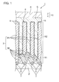
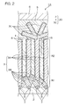
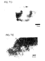
- the needle-like crystals 3 include first needle-like crystals 3A extending from respective plural starting points S positioned spaced apart from one another on the surface of the transparent electrode 2 at an angle of almost 90° with respect to the surface of the transparent electrode 2 (extending perpendicularly to the surface of the transparent electrode 2), and second needle-like crystals 3B extending from the respective starting points S in directions within a wider angular range encompassing a direction perpendicular to the surface of the transparent electrode 2 (for example, the angle produced with the surface of the transparent electrode 2 is 0° to 90°) and shorter than the first needle-like crystals 3A.
- the longitudinal directions and the c-axes coincide with each other.
- the first needle-like crystals 3A have almost the same length.
- a p-n junction is formed by the coating film 15, which is an n-type semiconductor, and the p-type semiconductor portion 5.
- Dye particles 8, which are a light absorbing material, are provided between the coating film 15 formed on the surface of the needle-like crystals 3 (n-type semiconductor) and the p-type semiconductor portion 5 (in the vicinity of the interface thereof).
- the photovoltaic conversion element 1 when light comes incident on the p-n junction portion from the transparent electrode 2 side, electron-hole pairs are generated at the p-n junction portion, and holes and electrons migrate to the counter electrode 6 and the transparent electrode 2, respectively. This gives rise to a photoelectric current (photoelectromotive force).
- the dye particles 8 function to assist an active layer (the needle-like crystals 3, the p-type semiconductor portion 5, and the coating film 15) for light absorption. It is therefore possible to absorb light introduced inside the element efficiently.
- the transparent electrode 2 serving as the base and the opposite side to the transparent electrode 2 with respect to the array 4 are isolated in a satisfactory manner virtually by the array 4 (needle-like crystals 3) alone, and no insulator for this isolation is provided among the needle-like crystals 3.
- This configuration increases the effective surface area of the needle-like crystals 3.
- no insulator is used to isolate the transparent electrode 2 side and the opposite side to the transparent electrode 2, neither an inconvenience resulting from deterioration or coloring of the insulator, nor diffusion of impurities into the device ascribed to the use of the insulator will occur in the photovoltaic conversion element (or light emitting element) 1.
- a single emission wavelength can be obtained when the third needle-like crystals 3C is covered with the coating film 15 substantially completely.
- the third needle-like crystals 3C is not completely covered with the coating film 15, light emission occurs at two points: light emission at the interface between the coating film 15 and the p-type semiconductor portion 5, and light emission at the interface between the needle-like crystals 3C and the p-type semiconductor portion 5.
- more than one peak wavelength is present in the emission spectrum.
- the third needle-like crystals 3C is covered with the coating film 15 substantially completely, light emission occurs only at the interface between the coating film 15 and the p-type semiconductor portion 5.
- the light emitting element therefore has a single emission wavelength.
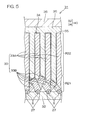
- the surface of the light receiving layer 9 (the surface on the opposite side to the surface of the needle-like crystals 3) is covered with the p-type semiconductor portion 5.
- a space between adjacent first needle-like crystals 3A is almost completely filled up with the light receiving layer 9 and the p-type semiconductor portion 5.
- the photovoltaic conversion element 11 is able to generate a photoelectric current using light absorbed in the light receiving layer 9.
- a leak current can be reduced by reducing the contact area of the light receiving layer 9 and the transparent electrode 2.
- holes are given to the transparent electrode 2 from the light receiving layer 9 at a certain probability.
- electrons are given to the transparent electrode 2 from the needle-like crystals 3. This increases the recombination probability of electrons and holes in the transparent electrode 2 and the luminescent efficiency is reduced. It is, however, possible to avoid such an event by reducing the contact area of the light receiving layer 9 and the transparent electrode 2.
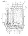
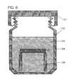
- the coating film 45 covers a large portion of the surface of the needle-like crystals 23 (first and second needle-like crystals 23A and 23B); however, it is absent in a closed space defined by the needle-like crystals 23 and the storage node 22.
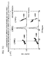
- a plurality of microscopic regions 27 made of crystals of zinc oxide are present between the storage node 22 and the array 24 (chiefly in the vicinity of the starting points S).
- the crystal orientations of the respective microscopic regions 27 are random and do not necessarily coincide with the crystal orientations of the needle-like crystals 23.
- the composites 10, 20, 30, and 40 can be obtained by letting the needle-like crystals 3, 23, and 33 be grown on the transparent electrode 2, the storage node 22, or the substrate 32 serving as the base by means of electroless plating using a plating solution (hereinafter, referred to as the "specific plating solution") containing at least one kind of alkali selected from the group consisting of X 1 OH, where X 1 is one of Na, K, and Cs, X 2 2 CO 3 , where X 2 is one of H, Na, K, and Cs, and NH 3 , and having a pH of 13 or higher.
- a plating solution hereinafter, referred to as the "specific plating solution”
- alkali selected from the group consisting of X 1 OH, where X 1 is one of Na, K, and Cs, X 2 2 CO 3 , where X 2 is one of H, Na, K, and Cs, and NH 3 , and having a pH of 13 or higher.
- the needle-like crystals 3, 23, and 33 grown from arbitrary starting points in directions far from a direction perpendicular to the surface of the base cannot be grown long as they are hindered by the needle-like crystals 3, 23, and 33 grown from other adjacent starting points, whereas the needle-like crystals 3, 23, and 33 grown in a direction almost perpendicular to the surface of the base can be grown long without being hindered by other needle-like crystals 3, 23, and 33.
- the longitudinal directions of the needle-like crystals 3, 23, and 33 as a whole are aligned.
- the arrays 4, 24, and 34 of the needle-like crystals 3, 23, and 33, respectively, are oriented with respect to the c-axes thereof.
- the producing method of the present invention it is possible to control the length and the density of the needle-like crystals 3, 23, and 33, for example, by controlling a time over which electroless plating is performed.
- the electrostatic capacity can be readily controlled.
- the coating films 15, 45 and 55 can be formed by means of sol-gel processing, dissolve separating, or recrystallization.
- the temperature of the solution was fixed to four types: 7°C, 15°C, 40°C, and 60°C, and the solution A was dropped with stirring into the solution B in which the array of needle-like crystals was dipped, after which stirring was continued for eight hours.
- the array was then taken out from the solution and rinsed with an ethanol solution, after which it was dried and calcined. An array of needle-like crystals on the surface of which was formed a coating film of titanium oxide was thus obtained.
- the calcination temperature in that instance was 450°C and the calcination time was 30 minutes.
Landscapes
- Chemical & Material Sciences (AREA)
- Engineering & Computer Science (AREA)
- Power Engineering (AREA)
- Electrochemistry (AREA)
- Materials Engineering (AREA)
- Metallurgy (AREA)
- Organic Chemistry (AREA)
- Inorganic Chemistry (AREA)
- Microelectronics & Electronic Packaging (AREA)
- Chemical Kinetics & Catalysis (AREA)
- Hybrid Cells (AREA)
- Crystals, And After-Treatments Of Crystals (AREA)
- Photovoltaic Devices (AREA)
- Inorganic Compounds Of Heavy Metals (AREA)
- Electroluminescent Light Sources (AREA)
- Luminescent Compositions (AREA)
- Oxygen, Ozone, And Oxides In General (AREA)
- Electric Double-Layer Capacitors Or The Like (AREA)
Applications Claiming Priority (2)
| Application Number | Priority Date | Filing Date | Title |
|---|---|---|---|
| JP2005160703 | 2005-05-31 | ||
| PCT/JP2006/310932 WO2006129733A1 (fr) | 2005-05-31 | 2006-05-31 | Composite comprenant un ensemble de cristal aciculaire, son procédé de production, élément de conversion photoélectrique, élément luminescent, et condensateur |
Publications (4)
| Publication Number | Publication Date |
|---|---|
| EP1900859A1 true EP1900859A1 (fr) | 2008-03-19 |
| EP1900859A8 EP1900859A8 (fr) | 2008-07-02 |
| EP1900859A4 EP1900859A4 (fr) | 2009-08-26 |
| EP1900859B1 EP1900859B1 (fr) | 2011-08-10 |
Family
ID=37481579
Family Applications (2)
| Application Number | Title | Priority Date | Filing Date |
|---|---|---|---|
| EP20060746986 Not-in-force EP1905874B1 (fr) | 2005-05-31 | 2006-05-30 | Complexe contenant une matrice de cristal aciculaire, son procede de production, element de conversion photoelectrique, element electroluminescent et condensateur |
| EP20060756852 Not-in-force EP1900859B1 (fr) | 2005-05-31 | 2006-05-31 | Composite comprenant un ensemble de cristal aciculaire, son procédé de production, élément de conversion photoélectrique, élément luminescent, et condensateur |
Family Applications Before (1)
| Application Number | Title | Priority Date | Filing Date |
|---|---|---|---|
| EP20060746986 Not-in-force EP1905874B1 (fr) | 2005-05-31 | 2006-05-30 | Complexe contenant une matrice de cristal aciculaire, son procede de production, element de conversion photoelectrique, element electroluminescent et condensateur |
Country Status (5)
| Country | Link |
|---|---|
| US (2) | US8207522B2 (fr) |
| EP (2) | EP1905874B1 (fr) |
| JP (2) | JP4880597B2 (fr) |
| CN (2) | CN101189367B (fr) |
| WO (2) | WO2006129650A1 (fr) |
Cited By (3)
| Publication number | Priority date | Publication date | Assignee | Title |
|---|---|---|---|---|
| WO2011062887A1 (fr) * | 2009-11-17 | 2011-05-26 | Corning Incorporated | Cellules solaires sensibilisées par colorant et procédé pour leur fabrication |
| US9853167B2 (en) | 2009-09-24 | 2017-12-26 | Semiconductor Energy Laboratory Co., Ltd. | Oxide semiconductor film and semiconductor device |
| US11177792B2 (en) | 2010-08-06 | 2021-11-16 | Semiconductor Energy Laboratory Co., Ltd. | Power supply semiconductor integrated memory control circuit |
Families Citing this family (22)
| Publication number | Priority date | Publication date | Assignee | Title |
|---|---|---|---|---|
| US8294025B2 (en) * | 2002-06-08 | 2012-10-23 | Solarity, Llc | Lateral collection photovoltaics |
| EP1905874B1 (fr) * | 2005-05-31 | 2013-03-27 | Kyocera Corporation | Complexe contenant une matrice de cristal aciculaire, son procede de production, element de conversion photoelectrique, element electroluminescent et condensateur |
| JP2008297168A (ja) * | 2007-05-31 | 2008-12-11 | National Institute Of Advanced Industrial & Technology | ZnOウィスカー膜及びその作製方法 |
| JP5136982B2 (ja) * | 2008-01-11 | 2013-02-06 | 独立行政法人産業技術総合研究所 | ZnOウィスカー膜、ZnOウィスカー膜形成のためのシード層及びそれらの作製方法 |
| GB0803702D0 (en) | 2008-02-28 | 2008-04-09 | Isis Innovation | Transparent conducting oxides |
| FR2932607B1 (fr) * | 2008-06-12 | 2011-01-14 | Commissariat Energie Atomique | Procede de passivation des centres de recombinaisons non radiatives d'echantillons en zno et echantillons en zno passive ainsi prepares |
| JP5069644B2 (ja) * | 2008-08-27 | 2012-11-07 | 旭化成株式会社 | 半導体結晶微粒子薄膜 |
| JP2011003399A (ja) * | 2009-06-18 | 2011-01-06 | Sharp Corp | 透明導電膜の製造方法および透明導電膜 |
| GB0915376D0 (en) | 2009-09-03 | 2009-10-07 | Isis Innovation | Transparent conducting oxides |
| JP5430419B2 (ja) * | 2010-01-20 | 2014-02-26 | 京セラ株式会社 | 光電変換モジュール |
| EP2543438B1 (fr) * | 2010-03-04 | 2017-05-03 | Panasonic Intellectual Property Management Co., Ltd. | Semi-conducteur optique, électrode semi-conductrice optique l'utilisant, cellule photoélectrochimique et système énergétique |
| CN102347144B (zh) * | 2010-07-28 | 2013-03-27 | 南美特科技股份有限公司 | 具有针状电极的光化学太阳能电池及其制造方法 |
| JP5969745B2 (ja) * | 2010-09-10 | 2016-08-17 | 株式会社半導体エネルギー研究所 | 半導体装置 |
| JP5189674B2 (ja) * | 2010-12-28 | 2013-04-24 | 出光興産株式会社 | 酸化物半導体薄膜層を有する積層構造、積層構造の製造方法、薄膜トランジスタ及び表示装置 |
| US8714691B2 (en) | 2012-05-29 | 2014-05-06 | Eastman Kodak Company | Detecting stretch or shrink in print media |
| US8721030B2 (en) | 2012-05-29 | 2014-05-13 | Eastman Kodak Company | Detecting stretch or shrink in print media |
| US9379261B2 (en) * | 2012-08-09 | 2016-06-28 | The Board Of Trustees Of The Leland Stanford Junior University | Ultra thin film nanostructured solar cell |
| US9214288B2 (en) | 2013-09-05 | 2015-12-15 | National Cheng Kung University | Flexible photo-anode of dye-sensitized solar cell and manufacturing method thereof |
| EP3159956B1 (fr) * | 2014-06-20 | 2021-11-03 | Sumitomo Metal Mining Co., Ltd. | Particules d'oxyde composite de lithium-nickel revêtues, et procédé de fabrication de particules d'oxyde composite de lithium-nickel revêtues |
| JP6005785B1 (ja) * | 2015-03-25 | 2016-10-12 | 株式会社東芝 | 光電変換素子およびその製造方法 |
| JP2017028251A (ja) * | 2015-07-23 | 2017-02-02 | パナソニックIpマネジメント株式会社 | 波長変換部材、光源装置、照明装置車両、および波長変換部材の製造方法 |
| JP2022014145A (ja) * | 2020-07-06 | 2022-01-19 | 東レエンジニアリング株式会社 | ナノワイヤ付きフィルム及びナノワイヤの製造方法 |
Family Cites Families (30)
| Publication number | Priority date | Publication date | Assignee | Title |
|---|---|---|---|---|
| KR920009567B1 (ko) * | 1987-12-29 | 1992-10-19 | 마쯔시다덴기산교 가부시기가이샤 | 산화아연위스커 및 그 제조방법 |
| US5362972A (en) * | 1990-04-20 | 1994-11-08 | Hitachi, Ltd. | Semiconductor device using whiskers |
| JP2697431B2 (ja) * | 1991-11-14 | 1998-01-14 | 松下電器産業株式会社 | 酸化亜鉛結晶及びその製造方法 |
| JPH06252360A (ja) | 1993-03-02 | 1994-09-09 | Hitachi Ltd | 半導体装置及びその製造方法 |
| DE69702277T2 (de) * | 1996-03-06 | 2001-03-01 | Canon K.K., Tokio/Tokyo | Verfahren zur Herstellung einer Dünnzinkoxidfilm und Verfahren zur Herstellung eines Substrats einer Halbleiteranordnung und Verfahren zur Herstellung einer photoelektrischen Umwandlungsvorrichtung unter Verwendung dieser Film |
| US6303945B1 (en) * | 1998-03-16 | 2001-10-16 | Canon Kabushiki Kaisha | Semiconductor element having microcrystalline semiconductor material |
| JP4097786B2 (ja) | 1998-06-02 | 2008-06-11 | 株式会社リコー | 太陽電池 |
| JP2001068649A (ja) | 1999-08-30 | 2001-03-16 | Toyota Central Res & Dev Lab Inc | 半導体記憶装置 |
| US6936484B2 (en) | 1998-10-16 | 2005-08-30 | Kabushiki Kaisha Toyota Chuo Kenkyusho | Method of manufacturing semiconductor device and semiconductor device |
| JP4109809B2 (ja) * | 1998-11-10 | 2008-07-02 | キヤノン株式会社 | 酸化チタンを含む細線の製造方法 |
| JP2000223167A (ja) | 1999-01-28 | 2000-08-11 | Fuji Photo Film Co Ltd | 光電変換素子および光電気化学電池 |
| US6580026B1 (en) * | 1999-06-30 | 2003-06-17 | Catalysts & Chemicals Industries Co., Ltd. | Photovoltaic cell |
| CN1213947C (zh) * | 1999-08-25 | 2005-08-10 | 昭和电工株式会社 | 高白色氧化锌微粒及其制造方法 |
| US6649824B1 (en) * | 1999-09-22 | 2003-11-18 | Canon Kabushiki Kaisha | Photoelectric conversion device and method of production thereof |
| JP4038963B2 (ja) | 2000-07-03 | 2008-01-30 | 三菱化学株式会社 | 光電変換素子 |
| JP3715911B2 (ja) * | 2000-09-21 | 2005-11-16 | キヤノン株式会社 | 酸化物針状結晶の製造方法、酸化物針状結晶および光電変換装置 |
| JP4313535B2 (ja) | 2001-01-26 | 2009-08-12 | 昭和電工株式会社 | 微粒子状酸化チタン複合体、同複合体の製造方法、同複合体組成物 |
| JP2002252359A (ja) | 2001-02-23 | 2002-09-06 | Seiko Epson Corp | 受光層および太陽電池 |
| JP2002356400A (ja) | 2001-03-22 | 2002-12-13 | Canon Inc | 酸化亜鉛の針状構造体の製造方法及びそれを用いた電池、光電変換装置 |
| JP2003151648A (ja) | 2001-11-14 | 2003-05-23 | Ulvac Japan Ltd | 可視光応答型酸化チタンを利用した太陽電池及びその作製方法 |
| JP2003243053A (ja) * | 2002-02-14 | 2003-08-29 | Canon Inc | 光電変換装置の製造方法 |
| JP2003321299A (ja) * | 2002-04-25 | 2003-11-11 | Canon Inc | 酸化亜鉛針状結晶及びその製造方法、並びにそれを用いた光電変換装置 |
| US7175762B1 (en) * | 2002-06-06 | 2007-02-13 | California Institute Of Technology | Nanocarpets for trapping particulates, bacteria and spores |
| JP2004060017A (ja) * | 2002-07-30 | 2004-02-26 | C Uyemura & Co Ltd | 無電解酸化亜鉛めっき方法 |
| AU2003302321A1 (en) * | 2002-09-12 | 2004-06-23 | The Trustees Of Boston College | Metal oxide nanostructures with hierarchical morphology |
| DE10254325A1 (de) * | 2002-11-21 | 2004-06-03 | Philips Intellectual Property & Standards Gmbh | Elektronisches Speicherbauteil |
| US7265037B2 (en) * | 2003-06-20 | 2007-09-04 | The Regents Of The University Of California | Nanowire array and nanowire solar cells and methods for forming the same |
| EP1690901A1 (fr) * | 2003-11-10 | 2006-08-16 | Kansai Paint Co., Ltd. | Matiere en poudre contenant une poudre inorganique monocristalline aciculaire, matiere de revetement, dispersion de poudre liquide et leur procede d'utilisation |
| US7276389B2 (en) * | 2004-02-25 | 2007-10-02 | Samsung Electronics Co., Ltd. | Article comprising metal oxide nanostructures and method for fabricating such nanostructures |
| EP1905874B1 (fr) * | 2005-05-31 | 2013-03-27 | Kyocera Corporation | Complexe contenant une matrice de cristal aciculaire, son procede de production, element de conversion photoelectrique, element electroluminescent et condensateur |
-
2006
- 2006-05-30 EP EP20060746986 patent/EP1905874B1/fr not_active Not-in-force
- 2006-05-30 US US11/916,014 patent/US8207522B2/en not_active Expired - Fee Related
- 2006-05-30 JP JP2007519002A patent/JP4880597B2/ja not_active Expired - Fee Related
- 2006-05-30 WO PCT/JP2006/310758 patent/WO2006129650A1/fr not_active Ceased
- 2006-05-30 CN CN2006800183561A patent/CN101189367B/zh not_active Expired - Fee Related
- 2006-05-31 WO PCT/JP2006/310932 patent/WO2006129733A1/fr not_active Ceased
- 2006-05-31 JP JP2007519050A patent/JP4880598B2/ja not_active Expired - Fee Related
- 2006-05-31 US US11/916,024 patent/US8013321B2/en not_active Expired - Fee Related
- 2006-05-31 CN CN2006800186818A patent/CN101194054B/zh not_active Expired - Fee Related
- 2006-05-31 EP EP20060756852 patent/EP1900859B1/fr not_active Not-in-force
Cited By (7)
| Publication number | Priority date | Publication date | Assignee | Title |
|---|---|---|---|---|
| US9853167B2 (en) | 2009-09-24 | 2017-12-26 | Semiconductor Energy Laboratory Co., Ltd. | Oxide semiconductor film and semiconductor device |
| US10418491B2 (en) | 2009-09-24 | 2019-09-17 | Semiconductor Energy Laboratory Co., Ltd. | Oxide semiconductor film and semiconductor device |
| WO2011062887A1 (fr) * | 2009-11-17 | 2011-05-26 | Corning Incorporated | Cellules solaires sensibilisées par colorant et procédé pour leur fabrication |
| US11177792B2 (en) | 2010-08-06 | 2021-11-16 | Semiconductor Energy Laboratory Co., Ltd. | Power supply semiconductor integrated memory control circuit |
| US11677384B2 (en) | 2010-08-06 | 2023-06-13 | Semiconductor Energy Laboratory Co., Ltd. | Semiconductor integrated circuit with semiconductor layer having indium, zinc, and oxygen |
| US12021530B2 (en) | 2010-08-06 | 2024-06-25 | Semiconductor Energy Laboratory Co., Ltd. | Semiconductor integrated circuit |
| US12273109B2 (en) | 2010-08-06 | 2025-04-08 | Semiconductor Energy Laboratory Co., Ltd. | Semiconductor integrated circuit |
Also Published As
| Publication number | Publication date |
|---|---|
| CN101194054B (zh) | 2011-09-28 |
| WO2006129650A1 (fr) | 2006-12-07 |
| EP1905874B1 (fr) | 2013-03-27 |
| CN101194054A (zh) | 2008-06-04 |
| EP1900859A8 (fr) | 2008-07-02 |
| JPWO2006129733A1 (ja) | 2009-01-08 |
| US20100038637A1 (en) | 2010-02-18 |
| WO2006129733A1 (fr) | 2006-12-07 |
| EP1905874A4 (fr) | 2009-08-26 |
| JP4880598B2 (ja) | 2012-02-22 |
| EP1900859A4 (fr) | 2009-08-26 |
| CN101189367A (zh) | 2008-05-28 |
| EP1900859B1 (fr) | 2011-08-10 |
| JPWO2006129650A1 (ja) | 2009-01-08 |
| US8013321B2 (en) | 2011-09-06 |
| US8207522B2 (en) | 2012-06-26 |
| JP4880597B2 (ja) | 2012-02-22 |
| EP1905874A1 (fr) | 2008-04-02 |
| CN101189367B (zh) | 2012-01-04 |
| US20100043859A1 (en) | 2010-02-25 |
Similar Documents
| Publication | Publication Date | Title |
|---|---|---|
| EP1900859B1 (fr) | Composite comprenant un ensemble de cristal aciculaire, son procédé de production, élément de conversion photoélectrique, élément luminescent, et condensateur | |
| Jia et al. | Inhibiting lattice distortion of CsPbI 3 perovskite quantum dots for solar cells with efficiency over 16.6% | |
| US6653701B1 (en) | Semiconductor device and production method thereof | |
| Rui et al. | Defect passivation and electrical conductivity enhancement in perovskite solar cells using functionalized graphene quantum dots | |
| Dou et al. | Toward highly reproducible, efficient, and stable perovskite solar cells via interface engineering with CoO nanoplates | |
| CN102412369B (zh) | 一种有机/无机杂化太阳电池及其制备方法 | |
| Sun et al. | Growth of single-crystalline rutile TiO 2 nanowire array on titanate nanosheet film for dye-sensitized solar cells | |
| Zhang et al. | Enhanced photocatalytic property of γ-CsPbI3 perovskite nanocrystals with WS2 | |
| KR20030020854A (ko) | 광전 장치 및 이의 제조방법 | |
| EP2190056B1 (fr) | Cellule solaire sensibilisée par un colorant | |
| Zhu et al. | Application of facile solution-processed ternary sulfide Ag8SnS6 as light absorber in thin film solar cells | |
| Jaffri et al. | Expounded photoelectric and electrochemical profiling of LRE3+: β‐Ta2O5 (Ln3+= Ce3+, Pr3+, Nd3+) for high performance in energy systems | |
| Li et al. | Solution‐Processed Multivalent Molybdenum Oxide Tailoring Band Alignment for Efficient Sb2S3 Solar Cells | |
| Jia et al. | Broadband NIR photoelectronic performance for sunlight‐induced photocurrent from (Na YF 4: Yb‐Er)/Bi OI hybrid films | |
| CN204927356U (zh) | 一种改良型纳米氧化锌片阵列钙钛矿型太阳能电池 | |
| Sun et al. | Efficiency enhanced rutile TiO 2 nanowire solar cells based on an Sb 2 S 3 absorber and a CuI hole conductor | |
| CN116854876B (zh) | 一种用于钙钛矿太阳能电池的共价有机框架材料及其制备方法 | |
| Burgos et al. | Electrodeposition of ZnO nanorods as electron transport layer in a mixed halide perovskite solar cell | |
| Kumar et al. | Thin‐Film Fabrication Techniques in Dye‐Sensitized Solar Cells for Energy Harvesting | |
| Luan et al. | Vertically aligned ZnO nanorods/CdS nanowires branched heterostructures: Cathodoluminescence properties and photovoltaic application | |
| EP2237339A2 (fr) | Électrode pour éléments de conversion photoélectrique, son procédé de fabrication et cellule solaire sensibilisée aux colorants | |
| KR101198310B1 (ko) | 2단계 수열합성 공정을 이용한 이산화티탄 나노선과 이산화티탄 나노입자가 하이브리드된 광전극의 제조방법 | |
| Xu et al. | Interface‐Triggered Bulk Electrical Coupling in SnO2 via Mesoscopic Chemical Reconfiguration for Scalable, High‐Efficiency Perovskite Photovoltaics | |
| Kumar et al. | Hybrid nanostructures for photovoltaics | |
| KR101198325B1 (ko) | 이산화티탄 나노선과 고비표면적 이산화티탄 메조기공 후막이 하이브리드된 광전극의 제조방법 |
Legal Events
| Date | Code | Title | Description |
|---|---|---|---|
| PUAI | Public reference made under article 153(3) epc to a published international application that has entered the european phase |
Free format text: ORIGINAL CODE: 0009012 |
|
| 17P | Request for examination filed |
Effective date: 20071220 |
|
| AK | Designated contracting states |
Kind code of ref document: A1 Designated state(s): AT BE BG CH CY CZ DE DK EE ES FI FR GB GR HU IE IS IT LI LT LU LV MC NL PL PT RO SE SI SK TR |
|
| RIN1 | Information on inventor provided before grant (corrected) |
Inventor name: YOSHIKAWA, SUSUMU Inventor name: ARANAMI, JUNJI,C/O KYOCERA CORPORATION |
|
| DAX | Request for extension of the european patent (deleted) | ||
| A4 | Supplementary search report drawn up and despatched |
Effective date: 20090727 |
|
| GRAP | Despatch of communication of intention to grant a patent |
Free format text: ORIGINAL CODE: EPIDOSNIGR1 |
|
| GRAS | Grant fee paid |
Free format text: ORIGINAL CODE: EPIDOSNIGR3 |
|
| GRAA | (expected) grant |
Free format text: ORIGINAL CODE: 0009210 |
|
| AK | Designated contracting states |
Kind code of ref document: B1 Designated state(s): AT BE BG CH CY CZ DE DK EE ES FI FR GB GR HU IE IS IT LI LT LU LV MC NL PL PT RO SE SI SK TR |
|
| REG | Reference to a national code |
Ref country code: GB Ref legal event code: FG4D |
|
| REG | Reference to a national code |
Ref country code: CH Ref legal event code: EP |
|
| REG | Reference to a national code |
Ref country code: IE Ref legal event code: FG4D |
|
| REG | Reference to a national code |
Ref country code: DE Ref legal event code: R096 Ref document number: 602006023698 Country of ref document: DE Effective date: 20111013 |
|
| REG | Reference to a national code |
Ref country code: NL Ref legal event code: VDEP Effective date: 20110810 |
|
| LTIE | Lt: invalidation of european patent or patent extension |
Effective date: 20110810 |
|
| PG25 | Lapsed in a contracting state [announced via postgrant information from national office to epo] |
Ref country code: NL Free format text: LAPSE BECAUSE OF FAILURE TO SUBMIT A TRANSLATION OF THE DESCRIPTION OR TO PAY THE FEE WITHIN THE PRESCRIBED TIME-LIMIT Effective date: 20110810 Ref country code: FI Free format text: LAPSE BECAUSE OF FAILURE TO SUBMIT A TRANSLATION OF THE DESCRIPTION OR TO PAY THE FEE WITHIN THE PRESCRIBED TIME-LIMIT Effective date: 20110810 Ref country code: LT Free format text: LAPSE BECAUSE OF FAILURE TO SUBMIT A TRANSLATION OF THE DESCRIPTION OR TO PAY THE FEE WITHIN THE PRESCRIBED TIME-LIMIT Effective date: 20110810 Ref country code: IS Free format text: LAPSE BECAUSE OF FAILURE TO SUBMIT A TRANSLATION OF THE DESCRIPTION OR TO PAY THE FEE WITHIN THE PRESCRIBED TIME-LIMIT Effective date: 20111210 Ref country code: PT Free format text: LAPSE BECAUSE OF FAILURE TO SUBMIT A TRANSLATION OF THE DESCRIPTION OR TO PAY THE FEE WITHIN THE PRESCRIBED TIME-LIMIT Effective date: 20111212 Ref country code: SE Free format text: LAPSE BECAUSE OF FAILURE TO SUBMIT A TRANSLATION OF THE DESCRIPTION OR TO PAY THE FEE WITHIN THE PRESCRIBED TIME-LIMIT Effective date: 20110810 |
|
| REG | Reference to a national code |
Ref country code: AT Ref legal event code: MK05 Ref document number: 519873 Country of ref document: AT Kind code of ref document: T Effective date: 20110810 |
|
| PG25 | Lapsed in a contracting state [announced via postgrant information from national office to epo] |
Ref country code: CY Free format text: LAPSE BECAUSE OF FAILURE TO SUBMIT A TRANSLATION OF THE DESCRIPTION OR TO PAY THE FEE WITHIN THE PRESCRIBED TIME-LIMIT Effective date: 20110810 Ref country code: LV Free format text: LAPSE BECAUSE OF FAILURE TO SUBMIT A TRANSLATION OF THE DESCRIPTION OR TO PAY THE FEE WITHIN THE PRESCRIBED TIME-LIMIT Effective date: 20110810 Ref country code: GR Free format text: LAPSE BECAUSE OF FAILURE TO SUBMIT A TRANSLATION OF THE DESCRIPTION OR TO PAY THE FEE WITHIN THE PRESCRIBED TIME-LIMIT Effective date: 20111111 Ref country code: AT Free format text: LAPSE BECAUSE OF FAILURE TO SUBMIT A TRANSLATION OF THE DESCRIPTION OR TO PAY THE FEE WITHIN THE PRESCRIBED TIME-LIMIT Effective date: 20110810 Ref country code: PL Free format text: LAPSE BECAUSE OF FAILURE TO SUBMIT A TRANSLATION OF THE DESCRIPTION OR TO PAY THE FEE WITHIN THE PRESCRIBED TIME-LIMIT Effective date: 20110810 Ref country code: SI Free format text: LAPSE BECAUSE OF FAILURE TO SUBMIT A TRANSLATION OF THE DESCRIPTION OR TO PAY THE FEE WITHIN THE PRESCRIBED TIME-LIMIT Effective date: 20110810 |
|
| PG25 | Lapsed in a contracting state [announced via postgrant information from national office to epo] |
Ref country code: BE Free format text: LAPSE BECAUSE OF FAILURE TO SUBMIT A TRANSLATION OF THE DESCRIPTION OR TO PAY THE FEE WITHIN THE PRESCRIBED TIME-LIMIT Effective date: 20110810 |
|
| PG25 | Lapsed in a contracting state [announced via postgrant information from national office to epo] |
Ref country code: SK Free format text: LAPSE BECAUSE OF FAILURE TO SUBMIT A TRANSLATION OF THE DESCRIPTION OR TO PAY THE FEE WITHIN THE PRESCRIBED TIME-LIMIT Effective date: 20110810 Ref country code: CZ Free format text: LAPSE BECAUSE OF FAILURE TO SUBMIT A TRANSLATION OF THE DESCRIPTION OR TO PAY THE FEE WITHIN THE PRESCRIBED TIME-LIMIT Effective date: 20110810 |
|
| PG25 | Lapsed in a contracting state [announced via postgrant information from national office to epo] |
Ref country code: IT Free format text: LAPSE BECAUSE OF FAILURE TO SUBMIT A TRANSLATION OF THE DESCRIPTION OR TO PAY THE FEE WITHIN THE PRESCRIBED TIME-LIMIT Effective date: 20110810 Ref country code: RO Free format text: LAPSE BECAUSE OF FAILURE TO SUBMIT A TRANSLATION OF THE DESCRIPTION OR TO PAY THE FEE WITHIN THE PRESCRIBED TIME-LIMIT Effective date: 20110810 Ref country code: EE Free format text: LAPSE BECAUSE OF FAILURE TO SUBMIT A TRANSLATION OF THE DESCRIPTION OR TO PAY THE FEE WITHIN THE PRESCRIBED TIME-LIMIT Effective date: 20110810 |
|
| PLBE | No opposition filed within time limit |
Free format text: ORIGINAL CODE: 0009261 |
|
| STAA | Information on the status of an ep patent application or granted ep patent |
Free format text: STATUS: NO OPPOSITION FILED WITHIN TIME LIMIT |
|
| PG25 | Lapsed in a contracting state [announced via postgrant information from national office to epo] |
Ref country code: DK Free format text: LAPSE BECAUSE OF FAILURE TO SUBMIT A TRANSLATION OF THE DESCRIPTION OR TO PAY THE FEE WITHIN THE PRESCRIBED TIME-LIMIT Effective date: 20110810 |
|
| 26N | No opposition filed |
Effective date: 20120511 |
|
| REG | Reference to a national code |
Ref country code: DE Ref legal event code: R097 Ref document number: 602006023698 Country of ref document: DE Effective date: 20120511 |
|
| PG25 | Lapsed in a contracting state [announced via postgrant information from national office to epo] |
Ref country code: MC Free format text: LAPSE BECAUSE OF NON-PAYMENT OF DUE FEES Effective date: 20120531 |
|
| REG | Reference to a national code |
Ref country code: CH Ref legal event code: PL |
|
| GBPC | Gb: european patent ceased through non-payment of renewal fee |
Effective date: 20120531 |
|
| PG25 | Lapsed in a contracting state [announced via postgrant information from national office to epo] |
Ref country code: LI Free format text: LAPSE BECAUSE OF NON-PAYMENT OF DUE FEES Effective date: 20120531 Ref country code: CH Free format text: LAPSE BECAUSE OF NON-PAYMENT OF DUE FEES Effective date: 20120531 |
|
| REG | Reference to a national code |
Ref country code: IE Ref legal event code: MM4A |
|
| REG | Reference to a national code |
Ref country code: FR Ref legal event code: ST Effective date: 20130131 |
|
| PG25 | Lapsed in a contracting state [announced via postgrant information from national office to epo] |
Ref country code: IE Free format text: LAPSE BECAUSE OF NON-PAYMENT OF DUE FEES Effective date: 20120531 Ref country code: GB Free format text: LAPSE BECAUSE OF NON-PAYMENT OF DUE FEES Effective date: 20120531 Ref country code: FR Free format text: LAPSE BECAUSE OF NON-PAYMENT OF DUE FEES Effective date: 20120531 Ref country code: ES Free format text: LAPSE BECAUSE OF FAILURE TO SUBMIT A TRANSLATION OF THE DESCRIPTION OR TO PAY THE FEE WITHIN THE PRESCRIBED TIME-LIMIT Effective date: 20111121 |
|
| PG25 | Lapsed in a contracting state [announced via postgrant information from national office to epo] |
Ref country code: BG Free format text: LAPSE BECAUSE OF FAILURE TO SUBMIT A TRANSLATION OF THE DESCRIPTION OR TO PAY THE FEE WITHIN THE PRESCRIBED TIME-LIMIT Effective date: 20111110 |
|
| PG25 | Lapsed in a contracting state [announced via postgrant information from national office to epo] |
Ref country code: TR Free format text: LAPSE BECAUSE OF FAILURE TO SUBMIT A TRANSLATION OF THE DESCRIPTION OR TO PAY THE FEE WITHIN THE PRESCRIBED TIME-LIMIT Effective date: 20110810 |
|
| PG25 | Lapsed in a contracting state [announced via postgrant information from national office to epo] |
Ref country code: LU Free format text: LAPSE BECAUSE OF NON-PAYMENT OF DUE FEES Effective date: 20120531 |
|
| PG25 | Lapsed in a contracting state [announced via postgrant information from national office to epo] |
Ref country code: HU Free format text: LAPSE BECAUSE OF FAILURE TO SUBMIT A TRANSLATION OF THE DESCRIPTION OR TO PAY THE FEE WITHIN THE PRESCRIBED TIME-LIMIT Effective date: 20060531 |
|
| REG | Reference to a national code |
Ref country code: DE Ref legal event code: R082 Ref document number: 602006023698 Country of ref document: DE Representative=s name: VIERING, JENTSCHURA & PARTNER PATENT- UND RECH, DE Ref country code: DE Ref legal event code: R082 Ref document number: 602006023698 Country of ref document: DE Representative=s name: VIERING, JENTSCHURA & PARTNER MBB PATENT- UND , DE |
|
| PGFP | Annual fee paid to national office [announced via postgrant information from national office to epo] |
Ref country code: DE Payment date: 20190521 Year of fee payment: 14 |
|
| REG | Reference to a national code |
Ref country code: DE Ref legal event code: R119 Ref document number: 602006023698 Country of ref document: DE |
|
| PG25 | Lapsed in a contracting state [announced via postgrant information from national office to epo] |
Ref country code: DE Free format text: LAPSE BECAUSE OF NON-PAYMENT OF DUE FEES Effective date: 20201201 |