EP1903344A1 - Schiebeblock und Handhabungsvorrichtung mit dem Schiebeblock - Google Patents
Schiebeblock und Handhabungsvorrichtung mit dem Schiebeblock Download PDFInfo
- Publication number
- EP1903344A1 EP1903344A1 EP07116691A EP07116691A EP1903344A1 EP 1903344 A1 EP1903344 A1 EP 1903344A1 EP 07116691 A EP07116691 A EP 07116691A EP 07116691 A EP07116691 A EP 07116691A EP 1903344 A1 EP1903344 A1 EP 1903344A1
- Authority
- EP
- European Patent Office
- Prior art keywords
- plate
- handler
- pushing
- test tray
- pushing block
- Prior art date
- Legal status (The legal status is an assumption and is not a legal conclusion. Google has not performed a legal analysis and makes no representation as to the accuracy of the status listed.)
- Withdrawn
Links
Images


Classifications
-
- G—PHYSICS
- G01—MEASURING; TESTING
- G01R—MEASURING ELECTRIC VARIABLES; MEASURING MAGNETIC VARIABLES
- G01R31/00—Arrangements for testing electric properties; Arrangements for locating electric faults; Arrangements for electrical testing characterised by what is being tested not provided for elsewhere
- G01R31/26—Testing of individual semiconductor devices
-
- G—PHYSICS
- G01—MEASURING; TESTING
- G01R—MEASURING ELECTRIC VARIABLES; MEASURING MAGNETIC VARIABLES
- G01R31/00—Arrangements for testing electric properties; Arrangements for locating electric faults; Arrangements for electrical testing characterised by what is being tested not provided for elsewhere
- G01R31/28—Testing of electronic circuits, e.g. by signal tracer
- G01R31/2851—Testing of integrated circuits [IC]
- G01R31/2893—Handling, conveying or loading, e.g. belts, boats, vacuum fingers
-
- H—ELECTRICITY
- H10—SEMICONDUCTOR DEVICES; ELECTRIC SOLID-STATE DEVICES NOT OTHERWISE PROVIDED FOR
- H10P—GENERIC PROCESSES OR APPARATUS FOR THE MANUFACTURE OR TREATMENT OF DEVICES COVERED BY CLASS H10
- H10P74/00—Testing or measuring during manufacture or treatment of wafers, substrates or devices
Definitions
- the present invention relates to a pushing block which enables a latch to hold in place or release a packaged chip in a socket of a test tray when loading or unloading the packaged chip upon and from the socket and a handler equipped with the pushing block.
- a handler puts packaged chips through a series of environmental, electrical, and reliability tests. These tests vary in type and specifications, depending on the customer and use of the packaged devices. The tests may be performed on all of the packages in a lot or on selected samples.
- the handler puts packaged chips into a test tray and supplies the test tray to a tester.
- the tester includes a test board with a plurality of sockets, performing an electrical test on the packaged chips.
- the packaged chips are inserted into the sockets of the test board for the electrical test.
- the handler puts the packaged chips into a test tray, i.e. a jig and inserting the packaged chips contained in a test tray into sockets of the test board.
- the handler sorts the packaged chips according to test results.
- the handler removes packaged chips from a user tray and put the removed packaged chips into sockets of the test tray.
- the handler transfers the test tray to the tester. (This is referred as to "a loading operation”.
- the handler removes tested packaged chips from the sockets of the test tray and the tested packaged chips to a user tray (This is referred as to "an unloading operation”)
- the handler includes a plurality of pickers picking up and transferring the packaged chips in the loading and unloading operations.
- the picker movably provided on a body of the handler, picks up, transfers, and places the packaged chips.
- Sockets into which the packaged chips are inserted, are arranged in rows and columns in the test tray.
- Each socket includes a latch holding the packaged chips in place. When the latch releases the packaged chip, the packaged chip may be removed from the socket.
- the conventional picker includes a pushing pin by which the latch is pushed to release the packaged chip.
- the pushing pin protrudes farther than a nozzle of the picker. This enables the pushing pin to push the latch before the nozzle comes in contact with the packaged chip, when the picker is moved down to insert or pick up the packaged chip into or from the socket.
- the pushing pin has to be provided to each of the pickers. This increases a size of the picker, and requires the picker to carry the pushing pin with it even when it is not moved down to insert or pick up the packaged chip into or from the socket.
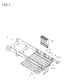
- a pushing block which enables the latch to release the packaged chip, as shown in FIG.1.
- the latch 30, including a button part 32 and a holding part 34, is provided to each of sockets of the test tray 20.
- the holding part 34 pushes the packaged chip inserted into the socket to hold it in place.
- the button part 32 is pushed by the pushing pin to enable the latch to release the packaged chip inserted into the socket.
- a rotating bar (not shown) is provided between the holding part 34 and the button part 32. So, when the pushing pin pushes an upper region of the button part 34, the holding part 34 is lifted, thus releasing the packaged chip. When the pushing pin withdraws from the button part 32, the latch returns to its original position by virtue of elastic force of a torsion spring, or a coil spring, thus holding the packaged chip in place.
- the pushing pin releases the latch 30.
- the latch holds the packaged chip in place to prevent it from being loose or deviating or dropping from the socket.
- the pushing pin 42 is provided on the pushing block 10. As shown in FIG.1, the pushing block 10 includes a pushing plate 40, on which a plurality of pushing pins is provided, and a cylinder block 60 moving up and down the pushing plate 40. Pushing pin 42 on the pushing plate 40 is as numerous as the latches on the test tray.
- the pushing plate 40 is moved up and down by the cylinder block 60.
- the cylinder block 60 includes a cylinder 62, a connecting rod 64, and a piston.
- the cylinder 62 is fixably provided on a frame 50 extending over an exchanging unit. An end of the connecting rod is connected to the piston and the other to the pushing plate 40. Reciprocating motion of the piston is changed to up-and-down motion of the pushing plate 40.
- the frame 50 includes a left frame 50A and a right frame 50B which are opposite to each other, in one pair.
- the up-and-down motion of the pushing plate 40 enables the pushing pin 42, which is provided on the pushing plate 40, to push and release the latch of socket.
- the pushing block 10 is provided over the test tray 20 on an exchanging unit. This makes it difficult to take corrective action when the picker fails to function properly, such as deviation of the packaged chip from the socket, and wrong insertion of the packaged chip into the socket. Furthermore, positioning of the pushing block 10 between the picker and the test tray causes interference between the picker and the pushing block, thus making the packaged chip deviate from the socket.
- the frame 50 has to be as wide as possible to minimize the interference between the picker and the pushing block 10.
- the cylinder block 60 is preferably provided only on the frame 50. This requires increase in a size of the pushing plate 40, thus increasing the number of the cylinder block 60 and a driving power driving the cylinder blocks 60.
- the middle of the pushing plate 40 tends to bend. This causes a malfunction of the picker.
- the pushing pin on the bent region of the pushing plate 40 fails to push the latch properly. As a result, the picker fails to pick up the packaged chip.
- a pushing plate guide 70 has to be additionally provided to guide up-and-down motion of the pushing plate 40.
- an object of the present invention is to provide a pushing block functioning properly without interference with a picker and a handler equipped with the pushing block.
- Another object of the present invention is to provide a pushing block having a simplified structure and a handler equipped with the pushing block.
- a pushing block for use in a handler including pushing pins, provided under a test tray, each pushing a latch upwards from under the test tray to enable the latch to release a packaged chip, a first plate on which the pushing pins are provided, and an assembly changing horizontal motion into vertical motion to move the first plate vertically.
- the assembly includes a cylinder base fixably provided on a body of the handler, a cylinder block including a cylinder fixably provided on a upper side of the cylinder base, and a connecting rod transferring reciprocal motion of a piston inside the cylinder, a third plate to which motion of the connecting rod is transferred, fourth plates, each having guide holes by which a direction of motion of the third plate is changed, moving rods, provided on lateral sides, moving along the guide holes, a second plate, supporting the first plate, and to which vertical motion of the third plate is transferred, and a cylinder base on which the cylinder block is fixably provided.
- a handler a test unit testing packaged chips
- a loading stacker where the packaged chips are loaded for testing
- an unloading stacker provided adjacent to the loading stacker, where the tested packaged chips, after sorted, are unloaded
- a test tray containing tested or not-tested packaged chips for transferring
- an exchanging unit where the packaged chips tested in the test unit are unloaded from the test tray and the not-tested packaged chips are loaded upon the test tray, at least one picker moving between the loading stacker and the exchanging unit, and between the exchanging unit and the unloading stacker, to transfer the tested or not-tested packaged chips
- a pushing block provided under the exchanging unit, including a first plate on which to provide pushing pins which release the packaged chip from the test tray, and an assembly moving the first plate vertically by changing vertical motion into horizontal motion.
- Positioning of the pushing block under the test tray prevents interference between the pushing block and the picker and makes it convenient to take corrective action when malfunction of the picker occurs. Furthermore, the pushing block is made compact.
- the whole bottom of the first plate is supported and pushed upwards, thus enabling all the pushing pins to open the latches uniformly at the same time.
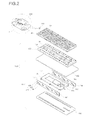
- FIG.2 is a perspective exploded view illustrating a pushing block 120 and a test tray which are for use in a handler, according to an embodiment of the present invention and a test tray.
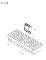
- FIG.3 is a perspective comprehensive view illustrating the pushing block 120 of FIG.2.
- the handler inserts packaged chips into a test tray and transfers the test tray containing the packaged chips to a tester.
- the handler unloads tested packaged chips from sockets of the test tray.
- the pushing block 120 is provided under the test tray 20.
- the test tray 20 is a jig which serves to contain the packaged chips for transfer.
- a plurality of sockets 110 is provided in rows and columns on the test tray 20.
- the socket 110 includes a latch which holds inserted packaged in place.
- the latch includes a holding part 114 holding the packaged chip, inserted into the socket, in place by pushing the packaged chip, and a butting part 112 releasing the holding part 114.
- the holding part 114 is moved as the button part 112 is moved. When the button part 112 is moved up, the holding part 114 is moved up, thus releasing the packaged chips.
- a rotating rod is provided on one side of the button part 112 and the holding part 114 is provided the other side of the button part 112. The rotating rod provides an axis about which the latch rotates when the pushing pin 132 moves up the button part 112.
- the pushing block 120 includes a first plate 130 on which the pushing pin 132 is provided, and an assembly 140 by which the first plate 130 is moved up and down.
- the pushing pins 132 on the first plate 130 may be as numerous as the latches on the test tray.
- the pushing pin 132 may further include a guide pin 134 guiding motion of the first plate for the pushing pins 132 to push the latches accurately.
- the guide pin 134 protrudes from the first plate 130 farther than the pushing pin 132.
- the holding part 114 is also moved up, thus releasing the packaged chip.
- the picker picks up the packaged chip from the socket, or inserts the packaged chip into the empty socket.
- the assembly 140 is provided under the first plate 130.
- the assembly 140 includes a second plate 182 supporting and holding the fist plate 130, a third plate 170 moving up and down the second plate 182, a cylinder block 160 transferring horizontal motion to the third plate 170, a pair of fourth plates 184 changing horizontal motion of the cylinder block 160 into vertical motion, and a cylinder base 150 on which the fourth plate is fixably provided.
- the cylinder base 150 is fixably provided on the body of the handler.
- the two fourth plates 184 are provided upright on two edges of the cylinder base 150, respectively, opposite to each other.
- the cylinder base 162 is fixably provided on the cylinder base 150 between the two fourth plates 184
- the third plate 170 is provided between the two fourth plates 184.
- the third plate 170 is a rectangular frame with the cylinder block 160 inside.
- the third plate 170 is connected to a piston inside the cylinder 162, with a connecting rod 164.
- Reciprocating motion of the piston causes reciprocating motion of the third plate 170.
- the fourth plate 184 has guide holes 185, each of which is longitudinal and inclined to a bottom of the fourth plate 184 with a predetermined angle.
- the horizontal motion of the third plate 170 is changed in the vertical motion of the third plate 170, using the guide holes 185 formed on the fourth plate 184.
- Moving rods 175, which are inserted into the guide holes 185, are provided on both lateral sides of the third plate 170. Accordingly, when the reciprocating motion of the piston is transferred to the third plate 170, the moving rods 175 are moved up along the guide holes 185. In this way, the motion of the third plate 170 is changed from horizontally to vertically.
- the moving rod 175 may further include a bearing 177.
- the bearing 177 facilitates sliding motion of the moving rod 175 along the guide hole 185.
- the guide hole 185 may further include an upper stopping hole 186 and a lower stopping hole 188.
- the guide hole 185 includes the upper stopping hole 185, the lower stopping hole 188, and the inclined longitudinal hole connecting between the upper and lower stopping holes 185 and the 188.
- the upper and lower stopping holes 186 and 188 serve to stop motion of the moving rod 175 along the guide hole 185. Furthermore, the upper and lower stopping holes 186 and 188 make motion of the moving rod 175 changed stably and smoothly.
- the upper and lower stopping holes 186 and 188 may be horizontally longitudinal. This makes it possible for the moving rod 175 to slide up along the guide hole 185 in a stable manner. That is, the third plate 175, which is supported by the third plate 170, is slopingly moved up in a stable manner,
- the fourth plate 184 may include a plurality of guide holes 185. Accordingly, the third plate 170 may include a plurality of moving rods 175.
- the third plate 170 applies a thrust force against the second plate 182 vertically.
- the second plate 182 supports the first plate 130 in a fixed manner.
- the second plate 182 may be wider that the first plate 130.
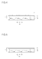
- FIG.4 is a view illustrating that the moving rod 175 arrives at the upper stopping hole 186 and stably stays there.
- FIG.5 is a view illustrating that the moving rod 175 arrives at the lower stopping hole 188 and stably stays there.
- a height of the first plate 130 get smaller by a vertical distance between the upper and lower stopping holes 186 and 188. This makes the pushing pin release the latch, thus closing the latch.
- the height of the first hole 130 gets larger by the vertical distance between the upper and lower stopping holes 186 and 188. This makes the pushing pin push the latch, thus opening the latch.
- FIG.6 is a perspective exploded view illustrating an embodiment of a socket 110 according to the present invention.
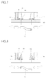
- FIGs 7 and 8 are cross-sectional views illustrating how the socket 110 of FIG.6 operates.
- the socket 110 includes a latch having a button part 110 and a holding part 114, a rotating rod 117 providing an axis about which the latch rotates, and a coil spring 118 returning the latch to its original position.
- the coil spring 118 makes the holding part 114 push the packaged chip inserted into the socket, when a predetermined amount of force isn't applied to the button part 112.
- the button part 112 and the holding part 114 are connected to the socket 110, with the rotating rod 117.
- the button part 112 and the holding part 114 are rotable about the axis of the rotating rod 117 with respect to the socket.
- the rotating rod 117 is positioned inside the rotating rod 117, to return the holding part 114 to its original position.
- FIG.7 when the latch remains closed by an elastic force of the coil spring, a groove 119 of the socket isn't allowed to receive the packaged chip.
- FIG.8 when the latch remains opened by a thrust force of pushing pin 132, the groove 119 of the socket is allowed to receive the packaged chip.
- the pushing pin 132 withdraws from the latch, the latch is closed by the elastic force of the coil spring.
- the operating mechanism of the latch having the button part 112 and the holding part 114 according to the present invention is not limited to the structures of the latches shown in FIGs 6 through 8.
- the button part 112 and the holding part 114 as one body, may be balanced in the middle, so that the button part 112 goes up and the holding part goes down, and vice versa.
- FIG.9 is a view illustrating a handler equipped with a pushing block according to the present invention.
- the handler according to an embodiment of the present invention includes a loading stacker 210, an unloading stacker 220, a test unit 240, pickers 250, and the pushing block provided under an exchanging unit.
- the loading stacker 210 is provided in the front. User trays, each of which contains not-tested packaged chips, are placed on the loading stacker 210.
- the unloading stacker 220 is provided adjacent to the loading stacker 210. Tested packaged chips, after sorted according to grades, are contained in their assigned user trays on the unloading stacker 220.
- the packaged chips in the user tray are contained in a test tray 222.
- the test tray 222 containing the packaged chips is transferred to the loading stacker 220.
- the handler may further include the exchanging unit 230.
- the exchanging unit 230 is an area where the not-tested packaged chips are loaded into the test tray, or the tested packaged chips are unloaded from the test tray.
- the buffer unit 260 is provided between the loading stacker 210 or the unloading stacker 220 and the exchanging unit 230.
- the buffer unit 260 temporarily receives the packaged chips transferred by the head assembly.
- the buffer unit includes a plate.
- the buffer units 260 may be provided next to both sides of the exchanging unit 230 which is provided in the middle of the main body of the handler. That is, the buffer unit 260 may include a loading buffer unit 260A and an unloading buffer unit 260B.
- the exchanging unit 230 is provided between the loading and unloading buffer units 260A and 260B.
- the buffer unit 260 may include two or more plates movable in an Y-axis direction.
- the picker 250 as shown in FIG.9, includes a first loading picker 250A moving between the loading stacker 210 and loading buffer unit 260A, a second loading picker 250B moving between the loading buffer unit 260A and the exchanging unit 230, a first unloading picker 250D moving between the unloading stacker 220 and the unloading buffer unit 260B, and a second unloading picker 250C moving between the exchanging unit 230 and the unloading buffer unit 260B.
- the pickers are movably provided to an X-axis and Y-axis gantry.
- the first loading picker 250A and the first unloading picker 250D may be movable in an X-axis or Y-axis direction
- the second loading picker 250B and the second unloading picker 250C may be movable in the X-axis direction.
- the test unit 240 is provided in the rear.
- the test unit 240 includes a heating-up chamber where the packaged chips are heated up, a test chamber where the packaged chips are tested, and a cooling-down chamber where the packaged chips are cooled down.
- the test tray containing the packaged chips goes through the heating-up chamber, the test chamber, and the cooling-down chamber, in the preceding order.
- the pushing block according to the present invention is provided under the exchanging unit.
- the pushing block is moved up to open the latch of the socket provided on the test tray, in order for the packaged chip to be inserted into or removed from the socket, when the test tray containing the packaged chips waits in the exchanging unit, to load or unload the packaged chip upon or from the test tray.
- the pushing block is moved down to close the latch of the socket provided to the test tray, in order for the packaged chip to be held in place, while the test tray is transferred to the test unit.
- the operation and structure of the pushing block is the same as above described.
Landscapes
- Engineering & Computer Science (AREA)
- Physics & Mathematics (AREA)
- General Physics & Mathematics (AREA)
- Computer Hardware Design (AREA)
- Microelectronics & Electronic Packaging (AREA)
- General Engineering & Computer Science (AREA)
- Testing Of Individual Semiconductor Devices (AREA)
- Container, Conveyance, Adherence, Positioning, Of Wafer (AREA)
Applications Claiming Priority (1)
| Application Number | Priority Date | Filing Date | Title |
|---|---|---|---|
| KR1020060092269A KR100839665B1 (ko) | 2006-09-22 | 2006-09-22 | 핸들러용 전자부품 고정해제 장치 및 이를 구비한 핸들러 |
Publications (1)
| Publication Number | Publication Date |
|---|---|
| EP1903344A1 true EP1903344A1 (de) | 2008-03-26 |
Family
ID=38616353
Family Applications (1)
| Application Number | Title | Priority Date | Filing Date |
|---|---|---|---|
| EP07116691A Withdrawn EP1903344A1 (de) | 2006-09-22 | 2007-09-18 | Schiebeblock und Handhabungsvorrichtung mit dem Schiebeblock |
Country Status (6)
| Country | Link |
|---|---|
| US (1) | US20080074120A1 (de) |
| EP (1) | EP1903344A1 (de) |
| JP (1) | JP4658106B2 (de) |
| KR (1) | KR100839665B1 (de) |
| CN (1) | CN100587495C (de) |
| TW (1) | TWI380394B (de) |
Families Citing this family (18)
| Publication number | Priority date | Publication date | Assignee | Title |
|---|---|---|---|---|
| KR101028774B1 (ko) * | 2008-11-13 | 2011-04-14 | 미래산업 주식회사 | 테스트 트레이 랫치 해제 유닛 |
| KR101304274B1 (ko) * | 2008-12-31 | 2013-09-26 | (주)테크윙 | 테스트 핸들러의 픽앤플레이스장치 |
| TWI401766B (zh) * | 2009-03-23 | 2013-07-11 | Evertechno Co Ltd | 試驗處理機及其零件移送方法 |
| KR101499573B1 (ko) * | 2010-06-16 | 2015-03-10 | (주)테크윙 | 테스트핸들러에서의 반도체소자 언로딩방법 |
| US20120249175A1 (en) * | 2011-03-31 | 2012-10-04 | Electro Scientific Industries, Inc. | Conveyor-mountable carrier for electronic device testing |
| KR101227773B1 (ko) * | 2011-07-05 | 2013-01-29 | 세크론 주식회사 | 테스트 핸들러용 래치 개방 장치 |
| JP2013145132A (ja) * | 2012-01-13 | 2013-07-25 | Advantest Corp | ハンドラ装置、試験方法 |
| KR101748256B1 (ko) * | 2014-03-25 | 2017-06-16 | 가부시키가이샤 어드밴티스트 | 핸들러 장치, 핸들러 장치의 조정 방법 및 시험 장치 |
| KR102312865B1 (ko) * | 2015-06-25 | 2021-10-14 | 세메스 주식회사 | 커스터머 트레이 로딩 유닛 |
| CN107052742A (zh) * | 2017-02-27 | 2017-08-18 | 桂林电子科技大学 | 一种符合动作经济原理的大型加工件脚踏式物料供给装置 |
| CN109425797B (zh) * | 2017-08-31 | 2024-10-11 | 上海新宇箴诚电控科技有限公司 | 一种基于LabVIEW的汽车门把手功能测试系统及方法 |
| KR102606650B1 (ko) * | 2018-04-23 | 2023-11-27 | (주)테크윙 | 픽커 팁 교환 장치 |
| CN110010568B (zh) * | 2019-04-16 | 2020-11-27 | 常州信息职业技术学院 | 微电子封装结构 |
| TWI726555B (zh) * | 2019-12-27 | 2021-05-01 | 致茂電子股份有限公司 | 下壓頭鎖定機構、及具備該機構之電子元件檢測設備 |
| KR102209062B1 (ko) * | 2020-03-03 | 2021-01-28 | 팸텍주식회사 | 반도체 소자 테스트 소켓의 래치 개폐 제어 장치 |
| KR102554635B1 (ko) * | 2021-04-12 | 2023-07-13 | (주)이즈미디어 | 카메라 모듈 검사용 소켓 개방장치 |
| CN114054385B (zh) * | 2021-11-11 | 2024-02-09 | 四川和恩泰半导体有限公司 | 全自动双头晶片测试机 |
| CN116298828B (zh) * | 2023-05-15 | 2023-10-13 | 合肥联宝信息技术有限公司 | 一种fct半自动测试机构 |
Citations (1)
| Publication number | Priority date | Publication date | Assignee | Title |
|---|---|---|---|---|
| EP1617230A1 (de) * | 2003-04-23 | 2006-01-18 | Advantest Corporation | Einlage für eine handhabungseinrichtung für elektronische komponenten, tablett und handhabungseinrichtung für elektronische komponenten |
Family Cites Families (12)
| Publication number | Priority date | Publication date | Assignee | Title |
|---|---|---|---|---|
| JPS62201377A (ja) * | 1986-02-28 | 1987-09-05 | Nippon Eng Kk | レ−ザのエ−ジング装置におけるプロ−ブ配設機構 |
| KR950006721B1 (ko) * | 1991-10-26 | 1995-06-21 | 주식회사코오롱 | 에스테르 반응관 |
| JPH065676A (ja) * | 1992-06-23 | 1994-01-14 | Hitachi Ltd | Icハンドラ |
| JP3097017B2 (ja) * | 1994-01-31 | 2000-10-10 | 株式会社ダイトー | Icハンドラーのキャリア構造 |
| KR19980069436A (ko) * | 1997-02-28 | 1998-10-26 | 김광호 | 테스트 핸들러의 캐리어 |
| JPH11165847A (ja) * | 1997-12-05 | 1999-06-22 | Hitachi Electron Eng Co Ltd | Icデバイス反転装置 |
| KR20000065297A (ko) * | 1999-04-01 | 2000-11-06 | 정문술 | 핸들러의 헤드핀 구조 |
| KR100298536B1 (ko) * | 1999-05-01 | 2001-09-26 | 정문술 | 테스트 핸들러의 캐리어 모듈 |
| US6636060B1 (en) * | 1999-07-16 | 2003-10-21 | Advantest Corporation | Insert for electric devices testing apparatus |
| JP4451992B2 (ja) * | 2001-02-28 | 2010-04-14 | 株式会社アドバンテスト | 試験用電子部品搬送媒体、電子部品試験装置および試験方法 |
| US6626682B2 (en) * | 2001-09-13 | 2003-09-30 | Earl W. Sausen | Integrated circuit device socket |
| KR100432355B1 (ko) * | 2001-11-17 | 2004-05-22 | 미래산업 주식회사 | 반도체 소자 테스트 핸들러의 테스트 트레이의 소자탈부착장치 |
-
2006
- 2006-09-22 KR KR1020060092269A patent/KR100839665B1/ko active Active
-
2007
- 2007-09-18 EP EP07116691A patent/EP1903344A1/de not_active Withdrawn
- 2007-09-20 US US11/858,560 patent/US20080074120A1/en not_active Abandoned
- 2007-09-21 TW TW096135560A patent/TWI380394B/zh not_active IP Right Cessation
- 2007-09-24 CN CN200710151320A patent/CN100587495C/zh active Active
- 2007-09-25 JP JP2007247496A patent/JP4658106B2/ja not_active Expired - Fee Related
Patent Citations (1)
| Publication number | Priority date | Publication date | Assignee | Title |
|---|---|---|---|---|
| EP1617230A1 (de) * | 2003-04-23 | 2006-01-18 | Advantest Corporation | Einlage für eine handhabungseinrichtung für elektronische komponenten, tablett und handhabungseinrichtung für elektronische komponenten |
Also Published As
| Publication number | Publication date |
|---|---|
| CN100587495C (zh) | 2010-02-03 |
| JP4658106B2 (ja) | 2011-03-23 |
| TWI380394B (en) | 2012-12-21 |
| US20080074120A1 (en) | 2008-03-27 |
| TW200828486A (en) | 2008-07-01 |
| JP2008076400A (ja) | 2008-04-03 |
| KR100839665B1 (ko) | 2008-06-19 |
| CN101149394A (zh) | 2008-03-26 |
| KR20080026972A (ko) | 2008-03-26 |
Similar Documents
| Publication | Publication Date | Title |
|---|---|---|
| US20080074120A1 (en) | Pushing block and and a handler with the pushing block | |
| US7495463B2 (en) | System and method for transferring trays within a test handler | |
| US20080075574A1 (en) | Picker and head assembly with the pickers | |
| KR101133188B1 (ko) | 소자소팅장치 및 그 방법 | |
| US6304073B1 (en) | IC testing apparatus | |
| CN100520426C (zh) | 电子部件处理装置用插件、托盘、及电子部件处理装置 | |
| US6636060B1 (en) | Insert for electric devices testing apparatus | |
| US7541828B2 (en) | Burn-in sorter and sorting method using the same | |
| US6248967B1 (en) | IC testing apparatus | |
| KR102401058B1 (ko) | 소자핸들러 | |
| KR20110018426A (ko) | 전자부품 시험방법, 인서트, 트레이 및 전자부품 시험장치 | |
| US20110199113A1 (en) | Insert containing apparatus for semiconductor package | |
| KR19980081510A (ko) | 반도체 디바이스용 트레이 꺼내기장치 및 반도체 디바이스용 트레이 수납장치 | |
| KR20100061570A (ko) | 인서트, 트레이 및 전자부품 시험장치 | |
| US20080071409A1 (en) | Handler | |
| JP4417470B2 (ja) | トレイ移送アーム、電子部品ハンドリング装置および電子部品試験装置 | |
| CN101290328B (zh) | 用于承载封装芯片的承载器及装备有该承载器的处理机 | |
| CN101842712B (zh) | 插入件、托盘及电子元件测试装置 | |
| KR100367336B1 (ko) | 커스터머 트레이 수납장치 | |
| JPH09181483A (ja) | Icデバイスの移載装置 | |
| KR19990065960A (ko) | 모듈아이씨(ic) 핸들러에서 소켓으로의 모듈아이씨 로딩 및언로딩장치 | |
| KR100295776B1 (ko) | 번인 테스터 소팅 핸들러의 트레이 운반장치 | |
| KR102710467B1 (ko) | 소자핸들러 | |
| KR102374397B1 (ko) | 메모리카드 이송핸들러 | |
| CN101290327B (zh) | 用于承载封装芯片的承载器及装备有该承载器的处理机 |
Legal Events
| Date | Code | Title | Description |
|---|---|---|---|
| PUAI | Public reference made under article 153(3) epc to a published international application that has entered the european phase |
Free format text: ORIGINAL CODE: 0009012 |
|
| 17P | Request for examination filed |
Effective date: 20070922 |
|
| AK | Designated contracting states |
Kind code of ref document: A1 Designated state(s): AT BE BG CH CY CZ DE DK EE ES FI FR GB GR HU IE IS IT LI LT LU LV MC MT NL PL PT RO SE SI SK TR |
|
| AX | Request for extension of the european patent |
Extension state: AL BA HR MK YU |
|
| RIN1 | Information on inventor provided before grant (corrected) |
Inventor name: HUR, JUNG Inventor name: CHOI, WAN-HEE Inventor name: KIM, SUN-HWAL Inventor name: AHN, JUNG-UG |
|
| AKX | Designation fees paid |
Designated state(s): AT BE BG CH CY CZ DE DK EE ES FI FR GB GR HU IE IS IT LI LT LU LV MC MT NL PL PT RO SE SI SK TR |
|
| 17Q | First examination report despatched |
Effective date: 20091030 |
|
| STAA | Information on the status of an ep patent application or granted ep patent |
Free format text: STATUS: THE APPLICATION IS DEEMED TO BE WITHDRAWN |
|
| 18D | Application deemed to be withdrawn |
Effective date: 20100310 |