EP1903553A2 - Flüssigkristallanzeige - Google Patents
Flüssigkristallanzeige Download PDFInfo
- Publication number
- EP1903553A2 EP1903553A2 EP07016071A EP07016071A EP1903553A2 EP 1903553 A2 EP1903553 A2 EP 1903553A2 EP 07016071 A EP07016071 A EP 07016071A EP 07016071 A EP07016071 A EP 07016071A EP 1903553 A2 EP1903553 A2 EP 1903553A2
- Authority
- EP
- European Patent Office
- Prior art keywords
- liquid crystal
- brightness
- image data
- data
- region
- Prior art date
- Legal status (The legal status is an assumption and is not a legal conclusion. Google has not performed a legal analysis and makes no representation as to the accuracy of the status listed.)
- Withdrawn
Links
Images




Classifications
-
- G—PHYSICS
- G02—OPTICS
- G02F—OPTICAL DEVICES OR ARRANGEMENTS FOR THE CONTROL OF LIGHT BY MODIFICATION OF THE OPTICAL PROPERTIES OF THE MEDIA OF THE ELEMENTS INVOLVED THEREIN; NON-LINEAR OPTICS; FREQUENCY-CHANGING OF LIGHT; OPTICAL LOGIC ELEMENTS; OPTICAL ANALOGUE/DIGITAL CONVERTERS
- G02F1/00—Devices or arrangements for the control of the intensity, colour, phase, polarisation or direction of light arriving from an independent light source, e.g. switching, gating or modulating; Non-linear optics
- G02F1/01—Devices or arrangements for the control of the intensity, colour, phase, polarisation or direction of light arriving from an independent light source, e.g. switching, gating or modulating; Non-linear optics for the control of the intensity, phase, polarisation or colour
- G02F1/13—Devices or arrangements for the control of the intensity, colour, phase, polarisation or direction of light arriving from an independent light source, e.g. switching, gating or modulating; Non-linear optics for the control of the intensity, phase, polarisation or colour based on liquid crystals, e.g. single liquid crystal display cells
- G02F1/133—Constructional arrangements; Operation of liquid crystal cells; Circuit arrangements
-
- G—PHYSICS
- G09—EDUCATION; CRYPTOGRAPHY; DISPLAY; ADVERTISING; SEALS
- G09G—ARRANGEMENTS OR CIRCUITS FOR CONTROL OF INDICATING DEVICES USING STATIC MEANS TO PRESENT VARIABLE INFORMATION
- G09G3/00—Control arrangements or circuits, of interest only in connection with visual indicators other than cathode-ray tubes
- G09G3/20—Control arrangements or circuits, of interest only in connection with visual indicators other than cathode-ray tubes for presentation of an assembly of a number of characters, e.g. a page, by composing the assembly by combination of individual elements arranged in a matrix no fixed position being assigned to or needed to be assigned to the individual characters or partial characters
- G09G3/34—Control arrangements or circuits, of interest only in connection with visual indicators other than cathode-ray tubes for presentation of an assembly of a number of characters, e.g. a page, by composing the assembly by combination of individual elements arranged in a matrix no fixed position being assigned to or needed to be assigned to the individual characters or partial characters by control of light from an independent source
- G09G3/36—Control arrangements or circuits, of interest only in connection with visual indicators other than cathode-ray tubes for presentation of an assembly of a number of characters, e.g. a page, by composing the assembly by combination of individual elements arranged in a matrix no fixed position being assigned to or needed to be assigned to the individual characters or partial characters by control of light from an independent source using liquid crystals
-
- G—PHYSICS
- G09—EDUCATION; CRYPTOGRAPHY; DISPLAY; ADVERTISING; SEALS
- G09G—ARRANGEMENTS OR CIRCUITS FOR CONTROL OF INDICATING DEVICES USING STATIC MEANS TO PRESENT VARIABLE INFORMATION
- G09G3/00—Control arrangements or circuits, of interest only in connection with visual indicators other than cathode-ray tubes
- G09G3/20—Control arrangements or circuits, of interest only in connection with visual indicators other than cathode-ray tubes for presentation of an assembly of a number of characters, e.g. a page, by composing the assembly by combination of individual elements arranged in a matrix no fixed position being assigned to or needed to be assigned to the individual characters or partial characters
- G09G3/34—Control arrangements or circuits, of interest only in connection with visual indicators other than cathode-ray tubes for presentation of an assembly of a number of characters, e.g. a page, by composing the assembly by combination of individual elements arranged in a matrix no fixed position being assigned to or needed to be assigned to the individual characters or partial characters by control of light from an independent source
- G09G3/36—Control arrangements or circuits, of interest only in connection with visual indicators other than cathode-ray tubes for presentation of an assembly of a number of characters, e.g. a page, by composing the assembly by combination of individual elements arranged in a matrix no fixed position being assigned to or needed to be assigned to the individual characters or partial characters by control of light from an independent source using liquid crystals
- G09G3/3611—Control of matrices with row and column drivers
- G09G3/3648—Control of matrices with row and column drivers using an active matrix
- G09G3/3666—Control of matrices with row and column drivers using an active matrix with the matrix divided into sections
-
- G—PHYSICS
- G09—EDUCATION; CRYPTOGRAPHY; DISPLAY; ADVERTISING; SEALS
- G09G—ARRANGEMENTS OR CIRCUITS FOR CONTROL OF INDICATING DEVICES USING STATIC MEANS TO PRESENT VARIABLE INFORMATION
- G09G2320/00—Control of display operating conditions
- G09G2320/02—Improving the quality of display appearance
- G09G2320/0233—Improving the luminance or brightness uniformity across the screen
-
- G—PHYSICS
- G09—EDUCATION; CRYPTOGRAPHY; DISPLAY; ADVERTISING; SEALS
- G09G—ARRANGEMENTS OR CIRCUITS FOR CONTROL OF INDICATING DEVICES USING STATIC MEANS TO PRESENT VARIABLE INFORMATION
- G09G2320/00—Control of display operating conditions
- G09G2320/02—Improving the quality of display appearance
- G09G2320/0285—Improving the quality of display appearance using tables for spatial correction of display data
-
- G—PHYSICS
- G09—EDUCATION; CRYPTOGRAPHY; DISPLAY; ADVERTISING; SEALS
- G09G—ARRANGEMENTS OR CIRCUITS FOR CONTROL OF INDICATING DEVICES USING STATIC MEANS TO PRESENT VARIABLE INFORMATION
- G09G2360/00—Aspects of the architecture of display systems
- G09G2360/14—Detecting light within display terminals, e.g. using a single or a plurality of photosensors
- G09G2360/145—Detecting light within display terminals, e.g. using a single or a plurality of photosensors the light originating from the display screen
- G09G2360/147—Detecting light within display terminals, e.g. using a single or a plurality of photosensors the light originating from the display screen the originated light output being determined for each pixel
-
- G—PHYSICS
- G09—EDUCATION; CRYPTOGRAPHY; DISPLAY; ADVERTISING; SEALS
- G09G—ARRANGEMENTS OR CIRCUITS FOR CONTROL OF INDICATING DEVICES USING STATIC MEANS TO PRESENT VARIABLE INFORMATION
- G09G3/00—Control arrangements or circuits, of interest only in connection with visual indicators other than cathode-ray tubes
- G09G3/20—Control arrangements or circuits, of interest only in connection with visual indicators other than cathode-ray tubes for presentation of an assembly of a number of characters, e.g. a page, by composing the assembly by combination of individual elements arranged in a matrix no fixed position being assigned to or needed to be assigned to the individual characters or partial characters
- G09G3/34—Control arrangements or circuits, of interest only in connection with visual indicators other than cathode-ray tubes for presentation of an assembly of a number of characters, e.g. a page, by composing the assembly by combination of individual elements arranged in a matrix no fixed position being assigned to or needed to be assigned to the individual characters or partial characters by control of light from an independent source
- G09G3/3406—Control of illumination source
Definitions
- the present disclosure relates to a liquid crystal display and, more particularly, to a liquid crystal display achieving brightness uniformity, thereby reducing manufacturing costs.
- liquid crystal displays include a thin film transistor (TFT) substrate having TFTs for switching pixels, a color filter substrate having color pixels, and a liquid crystal layer interposed between the TFT substrate and the color filter substrate.
- TFT thin film transistor
- Liquid crystal molecules constituting a liquid crystal layer are aligned according to an electric field generated between a TFT substrate and a color filter substrate, and a light transmissive index is changed according to the alignment of the liquid crystal molecules.
- Such LCDs are classified into edge-type LCDs and direct-type LCDs according to the position of a lamp used as a light source in a backlight module.
- Edge-type LCDs include at least one lamp disposed adjacent to a side surface of a light guide plate. Here, light emitted from the lamp is guided into a liquid crystal panel by the light guide plate.
- Direct-type LCDs include a plurality of lamps, and a reflective plate disposed below the lamps, which focuses light emitted from the lamps onto the display unit of a liquid crystal panel in order to maximize light utilization efficiency.
- the brightness of predetermined regions of a liquid crystal panel corresponding to regions where lamps are located is higher than that of other regions of the liquid crystal panel corresponding to spaces between the lamps, thereby resulting in non-uniformity in the overall brightness of the liquid crystal panel.
- the ratio of the distance between two adjacent lamps to the distance between the lamps and a diffusion plate must be maintained at 1.7 or less.
- the distance between the lamps and diffusion plate is often increased to a predetermined distance, which may increase the overall thickness of an LCD, thereby lengthening the driving chip package connecting the printed circuit board and the liquid crystal panel, which eventually increases the manufacturing cost.
- the distance between the lamps and diffusion plate may cause sagging in the diffusion plate due to its own weight.
- the sagging may worsen.
- Exemplary embodiments of the present invention provide a liquid crystal display achieving brightness uniformity, thereby reducing manufacturing costs.
- a liquid crystal display including a liquid crystal panel having a first region and a second region that exhibit different brightnesses when a predetermined data voltage is applied, a memory storing a reference brightness that is to be exhibited by the liquid crystal panel when the predetermined data voltage is applied, and a brightness correction unit receiving image data corresponding to the predetermined data voltage and correcting the image data so that the first region and the second region exhibit the reference brightness.
- FIG. 1 is an exploded perspective view illustrating a liquid crystal display according to an exemplary embodiment of the present invention.
- a liquid crystal display 10 includes a liquid crystal panel assembly 130, a backlight assembly 140, and an upper housing 110.
- the liquid crystal panel assembly 130 includes a liquid crystal panel 136 including a Thin Film Transistor (TFT) panel 133 and a common electrode panel 134, liquid crystals (not shown), gate tape carrier packages 131, data tape carrier packages 132, and a printed circuit board 135.
- TFT Thin Film Transistor
- the TFT panel 133 includes gate lines (not shown), data lines (not shown), an array of TFTs (not shown), pixel electrodes (not shown), etc.
- the common electrode panel 134 includes black matrices (not shown), a common electrode (not shown), etc., and is disposed opposite to the TFT panel 133.
- the gate tape carrier packages 131 are respectively connected to the gate lines in the TFT panel 133, and the data tape carrier packages 132 are respectively connected to the data lines in the TFT panel 133.
- Various driving devices for processing gate driving signals and data driving signals are mounted on the printed circuit board 135 so that the gate driving signals and the data driving signals are input to the gate tape carrier packages 131 and the data tape carrier packages 132, respectively.
- the backlight assembly 140 includes optical sheets 141, an optical plate 142, lamps 143, and a reflective plate 144.
- the lamps 143 may be LEDs (Light Emitting Diodes), CCFLs (Cold Cathode Fluorescent Lamps), EEFLs (External Electrode Fluorescent Lamps), and the like.
- the lamps 143 generate light by a lamp driving voltage applied to the lamps 143 from an external source (not shown).
- the lamps 143 are spaced apart from each other by a predetermined distance and positioned in parallel to each other at the same spacing.
- the lamps 143 may form a direct-type lamp structure. In order to achieve brightness uniformity by uniformly distributing a discharge gas in the lamps 143, the lamps 143 may be arranged horizontally with respect to the liquid crystal panel 136.
- the optical plate 142 may be disposed on the lamps 143 and serves to enhance the brightness uniformity of light generated from the lamps 143.
- the reflective plate 144 is disposed below the lamps 143 and reflects light upward from below the lamps 143.
- the reflective plate 144 may be formed integrally with the bottom surface of a lower housing 160. That is, if the lower housing 160 is made of a highly reflective material such as aluminum (Al) or aluminum alloy, the inner surface of the lower housing 160 itself can serve as the reflective plate 144.
- the optical sheets 141 are disposed on the optical plate 142 and serve to diffuse and focus light coming from the lamps 143.
- the optical sheets 141 include a diffusion sheet, a first prism sheet, a second prism sheet, and so on.
- the diffusion sheet is disposed above the lamps 143 and serves to enhance the brightness and uniformity of incident light from the lamps 143.
- the first prism sheet is disposed on the diffusion sheet.
- Pyramidal prisms (not shown) are uniformly arranged on a surface of the first prism sheet to focus light diffused from the diffusion sheet and to output the focused light.
- the first prism sheet may be a brightness enhancement film (BEF-TM, manufactured by 3M).
- the second prism sheet is disposed on the first prism sheet, and is a multi-layered, reflective, polarization prism sheet for focusing, polarizing, and outputting light.
- the second prism sheet may be a dual brightness enhancement film (DBEFTM, manufactured by 3M). If the first prism sheet can guarantee sufficient brightness and viewing angle, the second prism sheet may be omitted.
- DBEFTM dual brightness enhancement film
- the backlight assembly 140 includes a receiving frame 150 and the lower housing 160 for receiving the optical sheets 141, the optical plate 142, the lamps 143, and the reflective plate 144.
- the liquid crystal panel assembly 130 is disposed on the optical sheets 141, and is received in the lower housing 160 in a state in which it is supported by the receiving frame 150.
- the receiving frame 150 has sidewalls formed along its rectangular-shaped edges.
- the receiving frame 150 is constructed such that the liquid crystal panel assembly 130 can be supported by stepped portions or protrusions formed inside the sidewalls.
- the lower housing 160 has sidewalls formed along edges of its rectangular-shaped upper surface, and securely receives the backlight assembly 140 and the liquid crystal panel assembly 130 in an area defined by the sidewalls.
- the lower housing 160 also serves to prevent the bending of the optical sheets 141.
- the printed circuit board 135 of the liquid crystal panel assembly 130 is folded along an outer edge of the lower housing 160 so that it is disposed on a sidewall or a rear surface of the lower housing 160.
- the lower housing 160 can have a variety of shapes, depending on how the backlight assembly 140 or the liquid crystal panel assembly 130 is placed in the lower housing 160.
- the lower housing 160 is coupled to the upper housing 110 so that an upper surface of the liquid crystal panel assembly 130 received in the lower housing 160 is covered.
- a window (not shown) for exposing the liquid crystal panel assembly 130 to the outside is disposed on an upper surface of the upper housing 110.
- the upper housing 110 may be combined with the lower housing 160 by, but not limited to, a hook or screw connection method. Alternatively, the combining method of the upper housing 110 and the lower housing 160 may be modified in various manners.
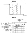
- FIG. 2 is a view illustrating brightness correction of image data according to an exemplary embodiment of the present invention.
- the liquid crystal panel When a constant data voltage is applied across a liquid crystal panel, the liquid crystal panel must show uniform brightness.
- the brightness a of predetermined regions of a liquid crystal panel corresponding to regions where lamps (see 143 of FIG. 1) are located is higher than the brightness b of other regions of the liquid crystal panel corresponding to spaces between the lamps, thereby resulting in brightness non-uniformity of the liquid crystal panel.
- image data in the predetermined regions of the liquid crystal panel corresponding to regions where the lamps are located are corrected to have a reference brightness c .
- the reference brightness c may be defined as the brightness b of the predetermined regions of the liquid crystal panel corresponding to the spaces between the lamps.
- line C in FIG. 2 the brightness of the predetermined regions of the liquid crystal panel corresponding to the regions where the lamps are located is reduced to that of the predetermined regions of the liquid crystal panel corresponding to the spaces between the lamps, resulting in uniform brightness over the entire area of the liquid crystal panel.
- a and B indicate the brightness value of the backlight assembly 140 before compensation
- C indicate the brightness value of the backlight assembly 140 after compensation.
- FIG. 3 is a block diagram illustrating a liquid crystal display according to an exemplary embodiment of the present invention.
- a liquid crystal display includes a liquid crystal panel 100, a driving voltage generator 200, a gate driver 300, a gamma voltage generator 400, a data driver 500, and a signal controller 600.
- the liquid crystal panel 100 includes a plurality of display signal lines G1-Gn and D1-Dm and a plurality of unit pixels that are connected to the display signal lines and arranged in matrix form.
- the display signal lines G1 - Gn and D1 - Dm include a plurality of gate lines G1-Gn receiving gate signals and a plurality of intersecting data lines D1 - Dm receiving data signals.
- the gate lines G1 - Gn extend substantially in a row direction and are substantially parallel to each other, while the data lines D1 - Dm extend substantially in a column direction and are substantially parallel to each other.
- Each of the plurality of pixels consists of a switching element Q connected to a corresponding one of the plurality of display signal lines G1 - Gn and D1 - Dm, a liquid crystal capacitor Clc and a storage capacitor Cst connected to the switching element Q. If necessary, the storage capacitor Cst may not be formed.
- the switching element Q is provided on a thin film transistor (TFT) substrate and has three terminals, a control terminal connected to one of the gate lines G1 - Gn, an input terminal connected to one of the data lines D1 - Dm, and an output terminal connected to both the liquid crystal capacitor Clc and the storage capacitor Cst, if employed.
- TFT thin film transistor
- the liquid crystal capacitor Clc includes a pixel electrode provided on the TFT substrate and a common electrode provided on a color filter substrate.
- the liquid crystal layer disposed between the two electrodes functions as a dielectric of the liquid crystal capacitor Clc.
- the pixel electrode is connected to the switching element Q, and the common electrode is connected to the common voltage Vcom and covers the entire surface of the color filter substrate.
- the common electrode may be provided on the TFT substrate, and both electrodes may have a bar or stripe shape.
- the storage capacitor Cst is defined by the overlap of the pixel electrode and a separate wire (not shown) provided on the TFT substrate and applied with a predetermined voltage such as the common voltage Vcom (separate wire type). Otherwise, the storage capacitor Cst is defined by the overlap of the pixel electrode and its previous gate line via an insulator (previous gate type).
- each pixel can represent its own color by providing one of a plurality of red, green and blue color filters in an area corresponding to the pixel electrode.
- the color filter is provided in the corresponding area of the color filter substrate.
- the color filters may be provided on or under the pixel electrode on the TFT substrate.
- a polarizer or polarizers (not shown) attached to at least one of the TFT substrate and the color filter substrate of the liquid crystal panel 100 convert the light polarization into the light transmittance.
- the driving voltage generator 200 generates a plurality of driving voltages. For example, the driving voltage generator 200 generates a gate-on voltage Von, a gate-off voltage Voff, and a common voltage Vcom (not shown).
- the gate driver 300 is connected to the gate lines G1-Gn of the liquid crystal panel 100 and provides gate signals to the gate lines G1-Gn, each gate signal being a combination of a gate-on voltage Von and a gate-off voltage Voff.
- the gamma voltage generator 400 generates two sets of a plurality of gray voltages related to the transmittance of the pixels.
- the data voltages in one set have a positive polarity with respect to the common voltage Vcom, while those in the other set have a negative polarity with respect to the common voltage Vcom.
- the positive-polarity data voltages and negative-polarity data voltages are alternately supplied to the liquid crystal panel 100 during inversion driving, which is well known.
- the data driver 500 is connected to the plurality of data lines D1-Dm of the liquid crystal panel 100.
- the data driver 500 generates gray voltages based on the plurality of voltages supplied from the gamma voltage generator 400, selects the generated gamma voltages, and applies the gamma voltages to each pixel as data signals.
- the data driver 500 typically includes a plurality of integrated circuits (ICs).
- the signal controller 600 generates control signals for controlling the gate driver 300, the data driver 500, and other components, and supplies the control signals to the corresponding components.
- the signal controller 600 includes a brightness correction unit 620 and provides the image data with uniform brightness supplied to the liquid crystal display. This will be described in more detail with reference to FIG.4
- the signal controller 600 is supplied by an external graphic controller (not shown) with RGB image-signals R, G and B and input control signals controlling the display of the LCD, for example, a vertical synchronization signal V sync , a horizontal synchronization signal H sync , a main clock MCLK, a data enable signal DE, and the like.
- the signal controller 600 generates a plurality of gate control signals CONT1 and a plurality of data control signals CONT2 and processes the image signals R, G and B for the liquid crystal panel 100 on the basis of the input control signals.
- the signal controller 600 provides the gate control signals CONT1 to the gate driver 300, the data control signals CONT2 and the processed image signals R', G' and B' to the data driver 500.
- the gate control signals CONT1 include a vertical synchronization start signal for indicating the start of a frame, a gate clock signal for controlling the output time of the gate-on voltage Von and an output enable signal for defining the widths of the gate-on voltage Von.
- the output enable signal and the gate clock signal are supplied to the driving voltage generator 200.
- the data control signals CONT2 include a horizontal synchronization start signal for indicating the start of a horizontal period, a load signal for instructing the data driver 500 to apply the appropriate data voltages to the data lines D1-Dm, an inversion control signal for reversing the polarity of the data voltages with respect to the common voltage Vcom, which is abbreviated as a data-voltage polarity, and a data clock signal.
- the data driver 500 receives a packet of the image data R', G' and B' for a pixel row from the signal controller 600 in response to the data control signal CONT2 received from the signal controller 600 and converts the image data R', G' and B' into data voltages selected from the gray voltages.
- the gate driver 300 applies the gate-on voltage Von to the gate line G1-Gn, thereby turning on the switching elements Q connected thereto.
- Liquid crystal molecules are aligned according to the electric field generated between a pixel electrode and a common electrode, and light passing through a liquid crystal layer is polarized accordingly. Such a change in polarization leads to a change in light transmittance that is induced by polarizers (not shown) attached to a TFT substrate and a color filter substrate.
- the gate-on voltage Von is sequentially applied to all the gate lines G1 to Gn, so that the data voltages are applied to all the pixels.
- the next frame starts, and a state of the reverse signal applied to the data driver 500 is controlled, so that the polarity of the data signal applied to each of the pixels is opposite to the polarity in the previous frame ("frame inversion").
- the data driver 5.00 may invert the polarities of the data voltages applied to the adjacent data lines D1 to Dm in one frame, so that the polarities of the pixel voltages of the pixels applied with the data voltages also change, which is referred to as "line inversion".
- the line inversion may become column inversion, which is referred to as "dot inversion”.
- FIG. 4 is a block diagram illustrating a signal controller 600 according to an exemplary embodiment of the present invention
- FIG. 5 is a block diagram illustrating a brightness correction unit 620 according to an exemplary embodiment of the present invention
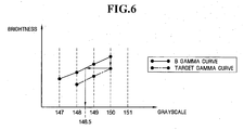
- FIG. 6 is a view illustrating a method of correcting image data according to an exemplary embodiment of the present invention.
- a signal controller 600 includes a memory 610 and the brightness correction unit 620.
- the memory 610 stores a reference brightness that is to be exhibited by a liquid crystal panel (see 100 of FIG. 3).
- the reference brightness may be defined as the brightness (see a of FIG. 2) of predetermined regions of a liquid crystal panel corresponding to regions where lamps are located or the brightness (see b of FIG. 2) of predetermined regions of the liquid crystal panel corresponding to spaces between the lamps.
- the memory 610 may be disposed inside the signal controller 600.
- the memory 610 may also be disposed outside the signal controller 600.
- the memory 610 may be a Read-Only Memory (ROM).
- the brightness correction unit 620 includes an R data correction unit 622, a G data correction unit 624, a B data correction unit 626, and R, G, and B multi-gradation units 632, 634, and 636 connected to the R, G, and B data correction portions 622, 624, and 626, respectively.
- the R, G, and B data correction portions 622, 624, and 626 convert the n-bit image data R, G, and B supplied from an external source (not shown) to predetermined m-bit image data according to the reference brightness stored in the memory 610 and then outputs the m-bit image data to the R, G, and B multi-gradation units 632, 634, and 636, respectively:
- the R, G, and B multi-gradation units 632, 634, and 636 convert the m-bit (m>n) image data to n-bit image data R', G', and B' , and then supply the n-bit image data R', G', and B' to the data driver 500.
- the R, G, and B multi-gradation units 632, 634, and 636 perform time-based dithering and frame rate control.
- the R, G, and B multi-gradation units 632, 634, and 636 may be provided as a single multi-gradation unit.
- the B image data of a grayscale corresponding to the desired brightness level must be input. That is, when the B image data corresponding to a 148.5-grayscale is input, a desired brightness can be obtained.
- a 150-grayscale B image data input from an external source must be corrected to a 148.5-grayscale B image data through a B data correction unit(see 626 of FIG. 5).
- image data supplied to the data driver 500 are expressed as n-bit data or slightly less than n-bit data.
- the R, G, and B multi-gradation units 632, 634, and 636 perform spatial dithering and time frame rate control for m-bit image data and then supply the dithered and frame rate controlled image data to the data driver 500.
- FIG. 7 is an illustration of dithering and frame rate control according to an exemplary embodiment of the present invention.
- 10-bit image data may be divided into upper 8-bit data and lower 2-bit data.
- the lower 2-bit data is "00", "01", “10”; or "11".
- all of the four adjacent pixels are expressed as upper 8-bit data.
- one of the four adjacent pixels is expressed as upper 8-bit+1 data.
- lower 2-bit data is set to "01" on average.
- the position of a pixel corresponding to the upper 8-bit+1 data can be shifted according to frames, as shown in FIG. 7.
- FIG. 7 illustrates that the position of a pixel corresponding to the upper 8-bit+1 data being shifted according to 4n, 4n+1, 4n+2, and 4n+3 frames.
- FIG. 8 is a view illustrating brightness correction of image data according to an exemplary embodiment of the present invention.
- the liquid crystal panel when a constant data voltage is applied to a liquid crystal panel (see 100 of FIG. 3), the liquid crystal panel must show uniform brightness.
- the brightness a of predetermined regions of a liquid crystal panel corresponding to regions where lamps are located is higher than the brightness b of predetermined regions of the liquid crystal panel corresponding to spaces between the lamps, thereby resulting in non-uniform brightness of the liquid crystal panel.
- image data in the predetermined regions of the liquid crystal panel corresponding to the spaces between the lamps are corrected to have a reference brightness c.
- the reference brightness c may be defined as the brightness a of the predetermined regions of the liquid crystal panel corresponding to the regions where the lamps are located.
- the brightness of the predetermined regions of the liquid crystal panel corresponding to the spaces between the lamps is equalized to that of the predetermined regions of the liquid crystal panel corresponding to the regions where the lamps are located, thereby resulting in uniform brightness over the entire area of the liquid crystal panel.
- a and B indicate the brightness value of the backlight assembly 140 before compensation
- C indicate the brightness value of the backlight assembly 140 after compensation.
- the signal controller 600 according to the exemplary embodiment of the present invention has substantially the same structure as the signal controller according to the exemplary embodiment described in relation to FIG. 4.
- a method of correcting image data according to the exemplary embodiment of the present invention may be performed in the same manner as described above with reference to FIG. 6 and, thus, a description thereof will be omitted.
- the signal controller 600 used for brightness correction of image data includes a memory (see 610 of FIG. 4) and a brightness correction unit (see 620 of FIG. 4).
- the memory stores a reference brightness that is to be exhibited by a liquid crystal panel (see 100 of FIG. 3).
- the reference brightness may be defined by brightness (see a of FIG. 8) of predetermined regions of a liquid crystal panel corresponding to regions where lamps are located or brightness (see b of FIG. 8) of predetermined regions of the liquid crystal panel corresponding to spaces between the lamps.
- the brightness correction unit includes an R data correction unit(see 622 of FIG. 5), a G data correction unit(see 624 of FIG. 5), a B data correction unit(see 626 of FIG. 5), and R, G, and B multi-gradation units (see 632, 634, and 636 of FIG. 5) connected to the R, G, and B data correction portions 622, 624, and 626, respectively.
- the R, G, and B data correction portions convert n-bit image data (see R, G, and B of FIG. 5) supplied from an external source to predetermined m-bit image data according to the reference brightness stored in the memory and then outputs the m-bit image data to the R, G, and B multi-gradation units, respectively.
- the R, G, and B multi-gradation units convert the m-bit (m>n) image data to n-bit image data (see R', G', and B' of FIG. 5) and then supply the n-bit image data to the signal controller 600.
- the R, G, and B multi-gradation units perform time-based dithering and frame rate control.
- the R, G, and B multi-gradation units may be provided as a single multi-gradation unit.
- a method of correcting image data according to the exemplary embodiment of the present invention may be performed in the same manner as described above with reference to FIG. 6 and, thus, a description thereof will be omitted.
- FIG. 9 is a view illustrating brightness correction of image data according to an exemplary embodiment of the present invention.
- the liquid crystal panel when a constant data voltage is applied to a liquid crystal panel (see 100 of FIG. 3), the liquid crystal panel must show uniform brightness.
- the brightness a of predetermined regions of a liquid crystal panel corresponding to regions where lamps are located is different from the brightness b of predetermined regions of the liquid crystal panel corresponding to spaces between the lamps, thereby resulting in non-uniform brightness of the liquid, crystal panel.
- image data in the predetermined regions of the liquid crystal panel corresponding to the regions where the lamps are located and image data in the predetermined regions of the liquid crystal panel corresponding to the spaces between the lamps are corrected to have a reference brightness c.
- the reference brightness c may be defined to be higher than the brightness b of the predetermined regions of the liquid crystal panel corresponding to the spaces between the lamps and lower than the brightness a of the predetermined regions of the liquid crystal panel corresponding to the regions where the lamps are located.
- the brightness of the predetermined regions of the liquid crystal panel corresponding to the regions where the lamps are located is equalized to that of the predetermined regions of the liquid crystal panel corresponding to the spaces between the lamps, thereby resulting in uniform brightness over the entire area of the liquid crystal panel.
- a and B indicate the brightness value of the backlight assembly 140 before compensation
- C indicate the brightness value of the backlight assembly 140 after compensation.
- the signal controller 600 according to the exemplary embodiment of the present invention has substantially the same structure as the signal controller according to the exemplary embodiment described in relation to FIG. 4.
- a method of correcting image data according to the exemplary embodiment of the present invention may be performed in the same manner as described above with reference to FIG. 6 and, thus, a description thereof will be omitted.
- the signal controller 600 used for brightness correction of image data includes a memory (see 610 of FIG. 4) and a brightness correction unit (see 620 of FIG. 4).
- the memory stores a reference brightness that is to be exhibited by a liquid crystal panel (see 100 of FIG. 3).
- the reference brightness may be defined to be higher than the brightness (see b of FIG. 9) of predetermined regions of the liquid crystal panel corresponding to spaces between lamps and lower than the brightness (see a of FIG. 9) of predetermined regions of the liquid crystal panel corresponding to the regions where the lamps are located.
- the brightness correction unit includes an R data correction unit(see 622 of FIG. 5), a G data correction unit(see 624 of FIG. 5), a B data correction unit(see 626 of FIG. 5), and R, G, and B multi-gradation units (see 632, 634, and 636 of FIG. 5) connected to the R, G, and B data correction portions, respectively.
- the R, G, and B data correction portions convert n-bit image data (see R, G, and B of FIG. 5) supplied from an external source to predetermined m-bit image data according to the reference brightness stored in the memory and then output the m-bit image data to the R, G, and B multi-gradation units, respectively.
- the R, G, and B multi-gradation units convert m-bit (m>n) image data to n-bit image data (see R', G', and B' of FIG. 5) and then supply the n-bit image data to the signal data driver 500.
- the R, G, and B multi-gradation units perform time-based dithering and frame rate control.
- the R, G, and B multi-gradation units may be provided as a single multi-gradation unit.
- liquid crystal displays according to the above-described exemplary embodiments of the present invention provide one or more of following advantages.
- a brightness correction unit is disposed in a signal controller, thereby achieving brightness uniformity over the entire area of a liquid crystal panel.
Landscapes
- Physics & Mathematics (AREA)
- Engineering & Computer Science (AREA)
- General Physics & Mathematics (AREA)
- Crystallography & Structural Chemistry (AREA)
- Chemical & Material Sciences (AREA)
- Theoretical Computer Science (AREA)
- Computer Hardware Design (AREA)
- Nonlinear Science (AREA)
- Mathematical Physics (AREA)
- Optics & Photonics (AREA)
- Control Of Indicators Other Than Cathode Ray Tubes (AREA)
- Liquid Crystal Display Device Control (AREA)
- Liquid Crystal (AREA)
Applications Claiming Priority (1)
| Application Number | Priority Date | Filing Date | Title |
|---|---|---|---|
| KR1020060090748A KR20080025931A (ko) | 2006-09-19 | 2006-09-19 | 액정 표시 장치 |
Publications (2)
| Publication Number | Publication Date |
|---|---|
| EP1903553A2 true EP1903553A2 (de) | 2008-03-26 |
| EP1903553A3 EP1903553A3 (de) | 2009-07-29 |
Family
ID=38828523
Family Applications (1)
| Application Number | Title | Priority Date | Filing Date |
|---|---|---|---|
| EP07016071A Withdrawn EP1903553A3 (de) | 2006-09-19 | 2007-08-16 | Flüssigkristallanzeige |
Country Status (5)
| Country | Link |
|---|---|
| US (1) | US20080068320A1 (de) |
| EP (1) | EP1903553A3 (de) |
| JP (1) | JP2008077041A (de) |
| KR (1) | KR20080025931A (de) |
| CN (1) | CN101149908A (de) |
Cited By (1)
| Publication number | Priority date | Publication date | Assignee | Title |
|---|---|---|---|---|
| EP2154674A1 (de) * | 2008-08-14 | 2010-02-17 | Samsung Electronics Co., Ltd. | Anzeigevorrichtung und Helligkeitsberichtigungsverfahren |
Families Citing this family (11)
| Publication number | Priority date | Publication date | Assignee | Title |
|---|---|---|---|---|
| TWI400692B (zh) * | 2008-08-05 | 2013-07-01 | Chunghwa Picture Tubes Ltd | 液晶顯示器及其影像資料處理裝置與方法 |
| CN101727843B (zh) * | 2008-10-10 | 2011-12-28 | 华映视讯(吴江)有限公司 | 液晶显示器及其影像数据处理装置与方法 |
| KR101479992B1 (ko) * | 2008-12-12 | 2015-01-08 | 삼성디스플레이 주식회사 | 전압 강하 보상 방법 및 그 시스템과 이를 포함한 표시 장치 |
| TWI410943B (zh) * | 2009-05-20 | 2013-10-01 | Chunghwa Picture Tubes Ltd | 可降低動態模糊之液晶顯示裝置 |
| WO2011050175A1 (en) * | 2009-10-21 | 2011-04-28 | Sarcode Corporation | Crystalline pharmaceutical and methods of preparation and use thereof |
| CN103366693A (zh) * | 2012-04-06 | 2013-10-23 | 联咏科技股份有限公司 | 亮度补偿方法及其区域调光电路与液晶显示器 |
| KR101352253B1 (ko) | 2012-04-24 | 2014-01-17 | 엘지디스플레이 주식회사 | 액정표시장치와 그 frc 방법 |
| KR102009724B1 (ko) | 2012-10-29 | 2019-08-13 | 삼성디스플레이 주식회사 | 플렉서블 표시 장치 및 표시 장치의 휘도 보정 방법 |
| CN102930842A (zh) * | 2012-10-30 | 2013-02-13 | 南京中电熊猫液晶显示科技有限公司 | 一种液晶显示器的色彩轨迹补偿方法 |
| CN104754277B (zh) * | 2013-12-27 | 2018-04-27 | 联想(北京)有限公司 | 信息处理设备及信息处理方法 |
| CN105374340B (zh) * | 2015-11-24 | 2018-01-09 | 青岛海信电器股份有限公司 | 一种亮度校正方法、装置和显示设备 |
Family Cites Families (7)
| Publication number | Priority date | Publication date | Assignee | Title |
|---|---|---|---|---|
| US6271825B1 (en) * | 1996-04-23 | 2001-08-07 | Rainbow Displays, Inc. | Correction methods for brightness in electronic display |
| KR100864420B1 (ko) * | 2000-11-30 | 2008-10-23 | 톰슨 라이센싱 | 디스플레이 드라이버 및 lcd/lcos 디스플레이를 구동하는 방법 |
| EP1650730B1 (de) * | 2004-10-25 | 2009-12-30 | Barco NV | Optische Korrektur für Leuchtpaneele mit hoher Gleichmäßigkeit |
| JP4904783B2 (ja) * | 2005-03-24 | 2012-03-28 | ソニー株式会社 | 表示装置及び表示方法 |
| JP4770619B2 (ja) * | 2005-09-29 | 2011-09-14 | ソニー株式会社 | 表示画像補正装置、画像表示装置、表示画像補正方法 |
| KR101182307B1 (ko) * | 2005-12-07 | 2012-09-20 | 엘지디스플레이 주식회사 | 평판표시장치와 그 화질 제어장치 및 화질 제어방법 |
| US20080068404A1 (en) * | 2006-09-19 | 2008-03-20 | Tvia, Inc. | Frame Rate Controller Method and System |
-
2006
- 2006-09-19 KR KR1020060090748A patent/KR20080025931A/ko not_active Withdrawn
-
2007
- 2007-01-10 JP JP2007002804A patent/JP2008077041A/ja active Pending
- 2007-08-16 EP EP07016071A patent/EP1903553A3/de not_active Withdrawn
- 2007-09-04 US US11/849,506 patent/US20080068320A1/en not_active Abandoned
- 2007-09-18 CN CNA2007101528202A patent/CN101149908A/zh active Pending
Cited By (1)
| Publication number | Priority date | Publication date | Assignee | Title |
|---|---|---|---|---|
| EP2154674A1 (de) * | 2008-08-14 | 2010-02-17 | Samsung Electronics Co., Ltd. | Anzeigevorrichtung und Helligkeitsberichtigungsverfahren |
Also Published As
| Publication number | Publication date |
|---|---|
| KR20080025931A (ko) | 2008-03-24 |
| JP2008077041A (ja) | 2008-04-03 |
| CN101149908A (zh) | 2008-03-26 |
| EP1903553A3 (de) | 2009-07-29 |
| US20080068320A1 (en) | 2008-03-20 |
Similar Documents
| Publication | Publication Date | Title |
|---|---|---|
| EP1903553A2 (de) | Flüssigkristallanzeige | |
| US7256763B2 (en) | Liquid crystal display device and driving method thereof | |
| US20100231617A1 (en) | Data processing device, liquid crystal display devce, television receiver, and data processing method | |
| US8610704B2 (en) | Display device and control method of the same | |
| EP1865489A2 (de) | Flüssigkristallanzeigevorrichtung und integrierter Schaltungschip dafür | |
| KR20100075074A (ko) | 디스플레이장치, 백라이트 유닛 및 상기 디스플레이 장치의구동 방법 | |
| CN102105928B (zh) | 数据处理装置、液晶显示装置、电视接收机以及数据处理方法 | |
| CN109785803B (zh) | 一种显示方法、显示单元及显示器 | |
| US7741784B2 (en) | Apparatus for driving a light source and liquid crystal display device using the same | |
| US20060125810A1 (en) | Display device and driving apparatus thereof | |
| US7746330B2 (en) | Circuit and method for improving image quality of a liquid crystal display | |
| US20080136804A1 (en) | Liquid crystal display | |
| KR102062914B1 (ko) | 3원색 표시장치 및 그의 픽셀데이터 랜더링 방법 | |
| US7724268B2 (en) | Liquid crystal display | |
| JP2013003479A (ja) | 液晶表示装置およびその駆動方法 | |
| JP4732070B2 (ja) | フィードフォワード回路部が具備される液晶表示装置 | |
| TWI410917B (zh) | 液晶顯示器 | |
| US8384645B2 (en) | Method for driving LCD panel and LCD using the same | |
| KR20110068321A (ko) | 표시 장치, 백라이트 유닛 및 백라이트 유닛 제어 방법 | |
| KR20080026824A (ko) | 액정 표시 장치 | |
| KR100935669B1 (ko) | 액정 표시 장치 | |
| KR20060018398A (ko) | 표시 장치, 표시 장치의 구동 방법 및 표시 장치용 광원의구동 장치 | |
| KR20080073421A (ko) | 액정 표시 장치 및 그의 구동 방법 | |
| KR20110038238A (ko) | 표시 장치 및 광원 구동 장치 | |
| KR20070009294A (ko) | 표시장치 |
Legal Events
| Date | Code | Title | Description |
|---|---|---|---|
| PUAI | Public reference made under article 153(3) epc to a published international application that has entered the european phase |
Free format text: ORIGINAL CODE: 0009012 |
|
| AK | Designated contracting states |
Kind code of ref document: A2 Designated state(s): AT BE BG CH CY CZ DE DK EE ES FI FR GB GR HU IE IS IT LI LT LU LV MC MT NL PL PT RO SE SI SK TR |
|
| AX | Request for extension of the european patent |
Extension state: AL BA HR MK YU |
|
| RIN1 | Information on inventor provided before grant (corrected) |
Inventor name: KIM, YOUNG-MI Inventor name: CHOI, SEONG-SIK Inventor name: RYU, HAN-JIN Inventor name: KIM, HUN-JOO |
|
| PUAL | Search report despatched |
Free format text: ORIGINAL CODE: 0009013 |
|
| AK | Designated contracting states |
Kind code of ref document: A3 Designated state(s): AT BE BG CH CY CZ DE DK EE ES FI FR GB GR HU IE IS IT LI LT LU LV MC MT NL PL PT RO SE SI SK TR |
|
| AX | Request for extension of the european patent |
Extension state: AL BA HR MK RS |
|
| AKX | Designation fees paid | ||
| STAA | Information on the status of an ep patent application or granted ep patent |
Free format text: STATUS: THE APPLICATION IS DEEMED TO BE WITHDRAWN |
|
| 18D | Application deemed to be withdrawn |
Effective date: 20100130 |
|
| REG | Reference to a national code |
Ref country code: DE Ref legal event code: 8566 |